Week 13 - Input devices
Assignment
- measure something: add a sensor to a microcontroller board that you have designed and read it
Input Sensors Selection
Phototransistor
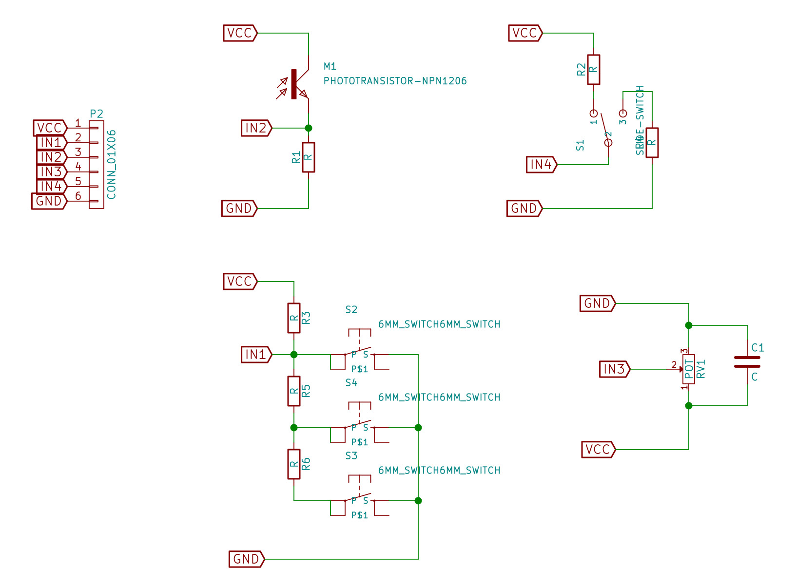
The first sensor I added is a Osram SFH 320 FA-3-Z, a NPN Silicium-based phototransistor especially suitable for sensitivity applications from 350 nm to 1100 nm
Phototransistors is a bi-terminal (emitter and collector) semiconductor device which has a light-sensitive base region: so it is similar to normal transistors except that its base current is replaced by light intensity. The current is generated when photons are absorbed in the phototransistor.
Tipical applications of phototransistors are miniature photointerrupters. So, the circuit to read the Phototransistor is a tipical switch circuit, where the transistor switches the input between Vcc and GND.
In the common collector configuration - or 'emitter follower' circuit - the emitter is taken to ground via a load resistor and the signal for the microcontroller being taken from the emitter connection of the phototransistor. So, the circuit generates an output that moves from the low state (0V) to a high state (>3.3V) when light is detected.
The phototransistor lets more current pass as more light shines on it. That current passes through the resistor, changing the voltage across it, so the voltage at the microcontroller changes with luminance.
WARNING
According to the datasheet, the small mark on the surface in the corner of this component marks the collector.At first I soldered the component in the wrong direction, but then I noticed that the notch in the package of the phototransistor represents the collector terminal, so I had to reverse it and put the collector next to the VCC
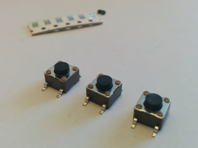
Push-Buttons Array
Push-Buttons are (ON)-OFF momentary switches, that is to say they only remain in their on state as long as they are being pressed. They usually come with a large button head and good tactile 'clicky' feedback when pushed, so they are best used for intermittent user-input cases (reset buttons, keypad etc).
I decided to add a series of TE Connectivity 2-1437565-8 buttons.
However, instead of using one pin per button, I used a voltage ladder to save pins. A voltage ladder is a simple electronic circuit consisting of several resistors connected in series, which is useful for providing a set of successive voltage references. Combining the ladder and buttons allows us to use multiple buttons and only one input pin, still being able to identify which button has been pressed!
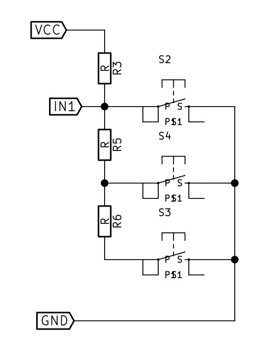
If no button is being pressed, the voltage on the analog pin IN1 will be pulled up to VCC (5V) by the R3 resistor and the the analog reading will be equal to 1023 (the upper limit of the 10-bits ADC of the AVR ATtiny). On the contrary, if the first switch S2 is pressed, IN1 will be short circuited to ground, and the reading will be 0. If the the second switch S4 is pressed, IN1 is being presented with a voltage that is divided between the R3 resistor that is trying to pull it up to 5V, and the R5 resistor pulling it to 0V: so the voltage will be 5V * R5/(R3+R5). Similarly, if we press S3, the voltage on the analog pin IN1 will be divided between the R3 resistor and the two R5 and R6 resistors in series (=R5 + R6).
WARNING
The voltage ladder correctly identify only one button at a time -- if you push more buttons simultaneously, the voltage at the pin will be the lowest among the button values.The values of the SMD resistor available in the lab was really limited (10K, 1K, 0.5K and 0.05K), so I decided to use only 1K resistors. As you can see below the calculus, the values are good enough to distinguish which button has been press
- none pressed: 5V * 1 = 5V --> 1023
- S2 pressed: 5V * 0 = 0V --> 0
- S4 pressed: 5V * (1000)/(1000+1000) = 2.5V --> 511
- S3 pressed: 5V * (1000+1000)/(1000+1000+1000) = 3.3V --> 682
Linear Temperature Sensor
As a temperature input I choose a Microchip MCP9701AT-E/TT, an analog active thermistor.
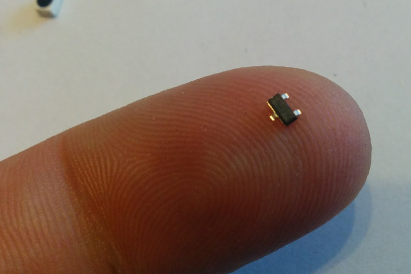
MCP9701AT-E/TT is a Linear Active Thermistor, an integrated circuit that convert temperature to analog voltage. It features an accuracy of ± 4°C from 0°C to +70°C while consuming 6 µA of operating current (so it's extremely low-power).
Unlike resistive sensors, e.g., thermistors, the Linear Active Thermistor IC does not require an additional signal-conditioning circuit. Therefore, the biasing circuit development overhead for thermistor solutions can be avoided by using this low-cost device. The Voltage Output pin (VOUT) can be directly connected to the ADC input of a microcontroller.
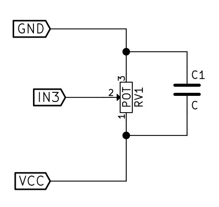
IC temperature sensors use analog circuitry to measure temperature. Unlike digital circuits, analog circuits are more susceptible to power-supply noise. As suggested in the Microchip Temperature Sensor Design Guide, it is recommended that a bypass capacitor C_bypass of 0.1 µf be placed at close proximity to the VDD and VSS pins of the sensor. The capacitor provides protection against power-supply glitches by slowing fast transient noise. Beware that, since its part of an RC filter, the effectiveness of the bypass capacitor depends upon the power-supply source resistance).
Switch selector
The switch is a component that can be used in a circuit to interrupt the current or to divert it from one path to another. I my board I used a CK Components AYZ0202AGRLC.
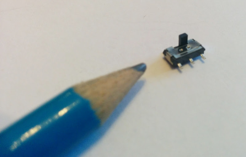
The switch is an ON-ON switch, that is a three-terminals components with one common and two switched positions: when one is on, the other is off (and vice versa). In one case, it short-circuits the left pin to the central one; on the contrary, when the selector is put on the right, it short circuit the central pin and the rightest one.
Hence, I have connected the central pin of the switch to the input pin, while the others are connected respectively to GND and VCC with two pull-up/down resistor. Hence, the switch can be seen as a digital input, which allows to set the input either to high (5V) or low (0).
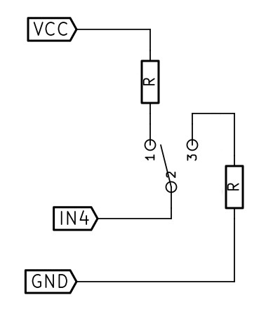
As an alternative, I might have connected directly the switch to VCC on one side and leave the other floating, using a pull down resistor for the input pin (likewise I did in week 6 for the button). However, this approach is more general: a switch could be use to select among two different sensors, or two different resistors (for example to change the sensitivity of the sensor, etc), so I though it was a good idea to test it during this week.
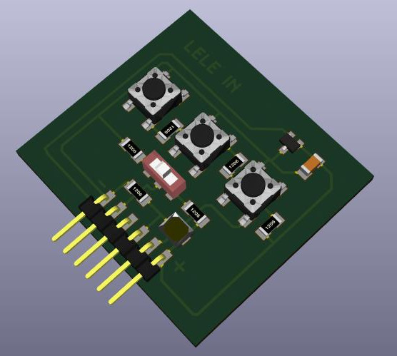
Board Design
As usual, I open KiCad, joined all the circuit for the different input a in a single schematics and connected all the input pin the the 6x1 male header using labels.
Then, I moved to Pcbnew and I started designing the PCB. I used the same size of the other modules (hellino core and hellino output) designed during week 10. The idea is to have a modular design, so you line up multiple modules.
I managed to put all the components on the PCB on a single side without using bridges: it took a few hours, but in the end I was very proud of this!
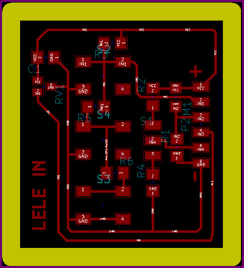
Before moving to the milling step, I rendered the final circuit using KiCad: it looked quite nice.
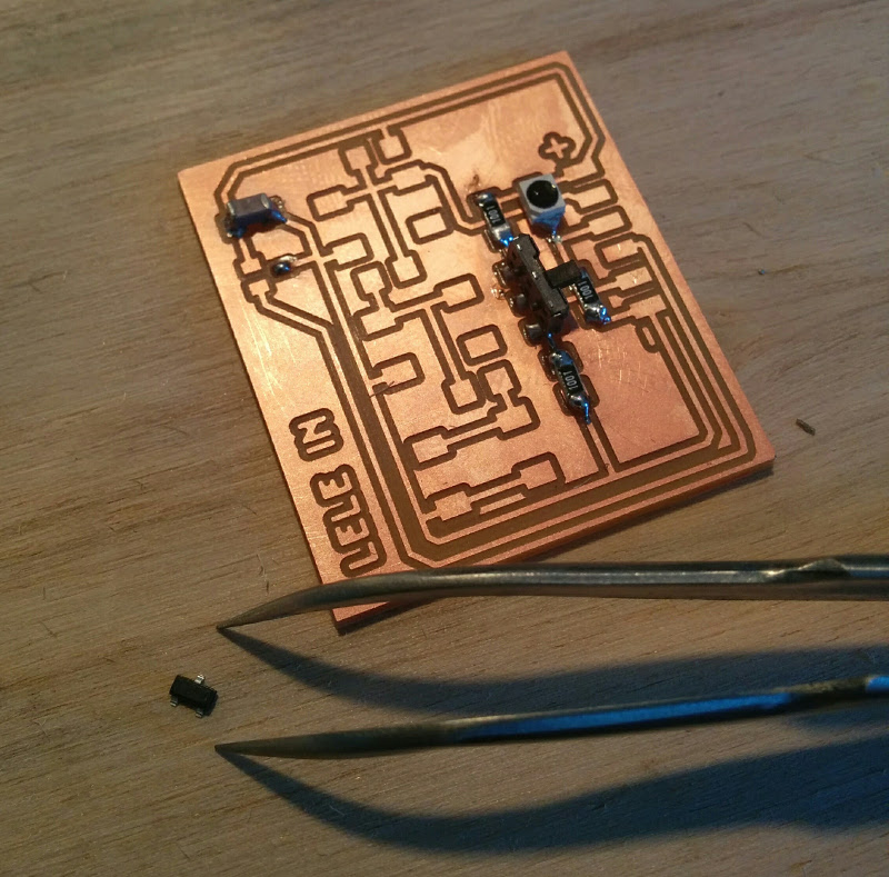
As usual, I exported the traces in SVG, and generated the cut files for the Roland MDX-40 using fabmodules.org and the parameters I described in week 10. After about 30 minutes I obtained my output module and I started soldering
Soldering was always a mixed-feelings experience, and I felt more like a pick-and-place machine than a fab academy student :-)
Eventually, I soldered everything and the board was ready: as you can see above, the KiCad render was quite realistic!
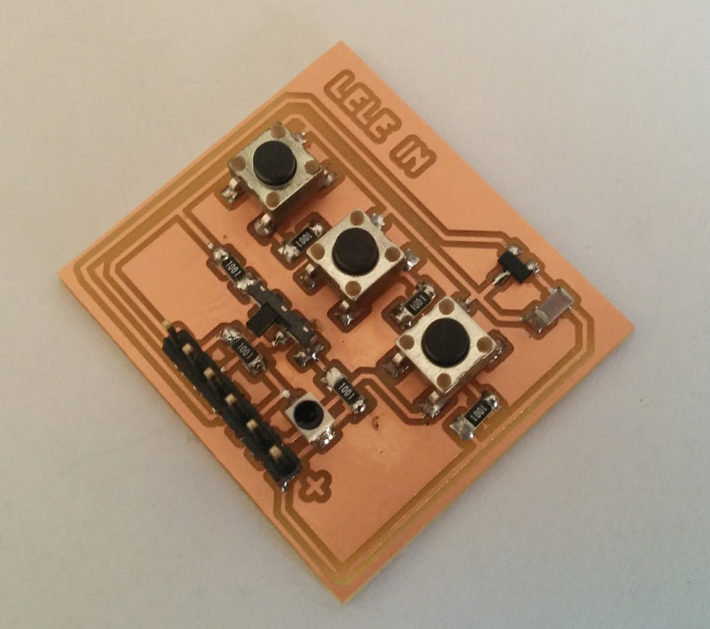
Now we are ready to connect the input module to the main board and read values!
Input Programming
First of all, I wanted to test the input in order to check if all sensors, switches and buttons were working correctly. Since the output board is a independent module, I attached its output to the input pin of an Arduino board.
int temp = 0;
int buttons = 0;
int photo = 0;
int swtch = 0;

void setup() {
  Serial.begin(9600);
  pinMode(A1, INPUT);  // pin header 1
  pinMode(6, INPUT);   // pin header 2
  pinMode(A0, INPUT);  // pin header 3
  pinMode(7, INPUT);   // pin header 4
}

void loop() {
  temp = analogRead(A0);
  buttons = analogRead(A1);
  photo = digitalRead(6);
  swtch = digitalRead(7);

  printVal("Temp", (temp*5000.0 / 1023 - 400)/19.5);
  printVal("Buttons", buttonPressed(buttons));
  printVal("Photo", photo);
  printVal("Switch", swtch);
  Serial.println();

  delay(1000);
}

void printVal(String name, int val) {
  Serial.print(name + ": " + val + "  ");
}

int buttonPressed(int val) {
  if (val < 10)   return 1;
  if (val < 520)  return 2;
  if (val < 700)  return 3;
  return 0;
}
And, when playing with buttons, switch and light, the output looked like this
Temp: 22  Buttons: 0  Photo: 0  Switch: 1
Temp: 21  Buttons: 1  Photo: 0  Switch: 1
Temp: 22  Buttons: 0  Photo: 0  Switch: 1
Temp: 20  Buttons: 3  Photo: 0  Switch: 1
Temp: 22  Buttons: 0  Photo: 0  Switch: 0
Temp: 20  Buttons: 0  Photo: 1  Switch: 0
Temp: 21  Buttons: 0  Photo: 0  Switch: 0
As you can see, this test showed that all the sensors were working fine. Two important things to note are how temperature and buttons are processed.
As for the temperature, the formula is provided by the datasheet (page 8):
V_out = T_c * T_a + V_0 where:
T_a = Ambient Temperature, V_out = Sensor Output Voltage, V_0 = Sensor Output Voltage at 0°C, T_c = Temperature Coefficient.
V_0 and T_c are DC Electrical Characteristics and are provided as-is: T_c = 19.5 mV/°C and V_0 = 400mV. Hence we can derive the ambient temperature with a bit of maths:
T_a = (V_out - V_0) / T_c
where V_out is the voltage. Since the ADC of the ATtiny is a 10-bit converter (0-1023) over a range 0V-5V, we can get the voltage V_out = 5000 mV / 1023 * ADC_val.
T_a = (temp * 5000.0 / 1023 - 400)/19.5
where temp is the value provided by the ADC reading.
The second interesting part is the buttonPressed() function, which converts the analog input to a button. Since we know the value associated to each button (see above), we can add a small safety-threshold (520 instead of 511, etc.) and identify which button has been pressed.
At this point, I moved to the ATtiny, in order to program my hellino board and read the values from the input board
In week 8 I showed how to extend the Arduino IDE to support third-party boards and additional microcontrollers. Specifically, I used the ATTinyCore project, which has created an extension for essentially every ATtiny processor that makes sense to use with Arduino (including the ATtiny44).
To add ATTinyCore, I installed the package from the IDE following the instructions posted on their repo, that is:
- File -> Preferences, enter the URL http://drazzy.com/package_drazzy.com_index.json in "Additional Board Manager URLs"
- Tools -> Boards -> Board Manager...
- Select ATtinyCore (Universal) and click "Install".
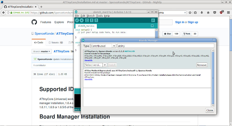
Then, I chose "ATtiny 24/44/84" from the list of Boards under the Tool menu, and I set the correct parameter for my design (choose yours carefully, especially the clock!)
- Board: ATtiny 24/44/84
- B.O.D: B.O.D. Disabled
- LTO: Disabled
- Pin mapping: Counterclockwise
- Chip: ATtiny44
- Clock: 8 MHz (internal)
- Programmer: USBtinyISP (ATtiny)
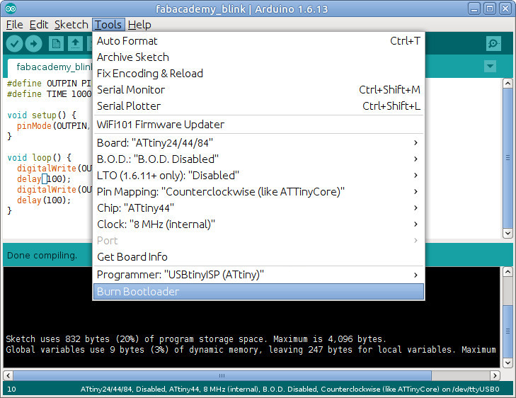
At this point, I had to burn the Bootloader to be able to program the chip directly from the IDE. Tools --> Burn Bootloader (and do not disconnect the board during this operation!). Beware that burning bootloader could overwrite your fuses: rewrite them with avrdude after this step.
I was ready to Verify and Upload my first code... Cool, no more Makefile for a while! :-)
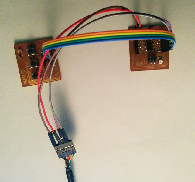
I connected my Output board to my Core Hellino board and I powered it through the FTDI cable.
At this point, I changed the pins in the code, moved to the software serial library, compiled the sketch again and... ERROR!!! Sketch too big; see http://www.arduino.cc/en/Guide/Troubleshooting#size for tips on reducing it.
As suggested in the page pointed by the error, floating point math is an issue with ATtiny/ATmega microcontrollers: they do not have a floating point unit, so each operations is done in software (and the code needed to perform a floating point division can be too huge for an ATtiny!)
The program space memory used was 4660 bytes (113%); I tried to remove the math from the temperature sensor line and the size of the binary lowered to 3262 bytes (79%). So the issue was clearly with this line. Hence, using a bit of math, firstly I removed one division and rounded everything to natural numbers: this led to a 3610 byte (88%) binary. Good but not enough! I was still using natural but quite big numbers, so I was doing math with long and not with integers. I simplified again and finally I obtained a binary of just 3278 bytes (80%)!
The results and the formulas are show in this table:
| Formula | Size [bytes] | |
|---|---|---|
| Floating point | (adc_val * 5000 / 1023 - 400) / 19.5 | 1056 bytes |
| Long (values up to 2,147,483,647) | (adc_val * 4888 - 400000) / 19500 | 348 bytes |
| Int (values up to 32,767) | (adc_val * 25 - 2050) / 100 | 16 bytes |
#include <SoftwareSerial.h>

SoftwareSerial mySerial(PIN_A0, PIN_A1);

#define PIN_BUTTON A2
#define PIN_PHOTO A3
#define PIN_TEMP A4
#define PIN_SWT A5

void setup() {
  mySerial.begin(9600);
  pinMode(PIN_BUTTON, INPUT);
  pinMode(PIN_PHOTO, INPUT);
  pinMode(PIN_TEMP, INPUT);
  pinMode(PIN_SWT, INPUT);
}

void loop() {
  mySerial.print("Temp: ");
  mySerial.print((analogRead(PIN_TEMP) * 25 - 2050) / 100);
  mySerial.print("  Button: ");
  mySerial.print(buttonPressed(analogRead(PIN_BUTTON)));
  mySerial.print("  Photo: ");
  mySerial.print(analogRead(PIN_PHOTO)>800?1:0);
  mySerial.print("  Switch: ");
  mySerial.print(digitalRead(PIN_SWT));
  mySerial.println();
  delay(1000);
}

int buttonPressed(int val) {
  if (val < 10)   return 1;
  if (val < 520)  return 2;
  if (val < 700)  return 3;
  return 0;
}
As you can see from the picture, I connected the FTDI orange cable (TX) to PIN_A0 (RX) and the FTDI yellow (RX) to PIN_A1. Then, I open the terminal with:
picocom -b 9600 /dev/ttyUSB0
and I started seeing the data flowing through the FTDI cable!
Temp: 23  Button: 0  Photo: 1  Switch: 1
Temp: 23  Button: 0  Photo: 1  Switch: 1
Temp: 23  Button: 2  Photo: 0  Switch: 1
Temp: 23  Button: 0  Photo: 0  Switch: 1
Temp: 23  Button: 1  Photo: 0  Switch: 1
Finally I closed picocom with CTRL+A CTRL+X (like screen).
Integer Math - Error analisys
I decided to investigate the measurement error added by integer math. I wrote a small python script and investigated the RMSE (Root Mean Square Error) when sampling values from -10 to +70 °C.
import numpy as np
import matplotlib.pyplot as plt

volt_min = 42
volt_max = 362

fp = []; longint = []; integ = []

adc = np.arange(volt_min, volt_max+1)

for t in list(adc):
	fp.append((t*5000 / 1023 - 400)/19.5)
	longint.append((t*4888 - 400000)//19500)
	integ.append((t*25 - 2050)//100)

print("RMSE int", np.sqrt(np.mean((np.array(fp)-np.array(integ))**2)))

plt.plot(adc, np.array(fp), 'r-', adc, np.array(longint), 'b-', adc, np.array(integ), 'g-')
plt.show()
A zoom on the plot clearly shows the distance between the real (red) and the integer (green), and the stairs behavior due to integer flooring is evident.
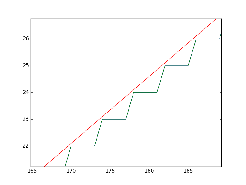
However, the RMSE obtained is 0.5688: a value which is acceptable for many non-critical applications.
Download zone - List of files
- input.zip Input board - KiCad project
- input_cut.zip Input board - SVG + PNG traces
- input_code.tar.gz Code for reading inputs