Datasheet
1.Study of datasheet ATTINY44
Need of datasheet reading
(from datasheet)A datasheet, is a document that summarizes the performance and other technical characteristics of a product, machine, component (e.g., an electronic component), material, a subsystem (e.g., a power supply) or software in sufficient detail to be used by a design engineer to integrate the component into a system.
The datasheet of ATTINY44 is large in that I study the some important points such as, ATTINY44
1. Pin Configurations
2. Pin Descriptions
3. Block Diagram of attiny44
4. Memories
5. Clock System
6. Power Management and Sleep Modes
7. System Control and Reset
8. Interrupts
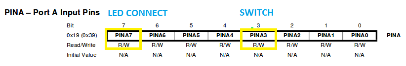
9. I/O Ports
10. Analog to Digital Converter
It is having high-performance, low-power Microchip AVR RISC-based CMOS 8-bit microcontroller combines 4KB ISP flash memory, 256-Byte EEPROM, 256B SRAM, 12 general purpose I/O lines, 32 general purpose working registers, an 8-bit timer/counter with two PWM channels, a 16-bit timer/counter with two PWM channels, internal and external interrupts, an 8-channel 10-bit A/D converter, a programmable gain stage (1x, 20x) for 12 differential ADC channel pairs, programmable watchdog timer with internal oscillator, a internal calibrated oscillator, and three software selectable power saving modes
Pin Configurations
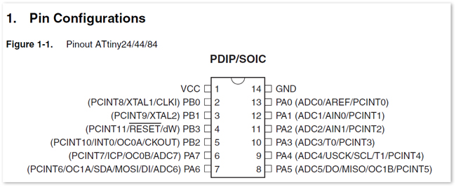
Pin discription- VCC ---Supply voltage.
GND ---Ground.
RESET---Reset input. A low level on this pin for longer than the minimum pulse length will generate a
reset, even if the clock is not running and provided the reset pin has not been disabled
Port B (PB3:PB0)---Port B is a 4-bit bi-directional I/O port with internal pull-up resistors.
Port A (PA7:PA0)---Port A is a 8-bit bi-directional I/O port with internal pull-up resistors (selected for each bit)
According with pin configration i connect led to analog pin 7 and button to the pin analog pin 7
Block Diagram of attiny44
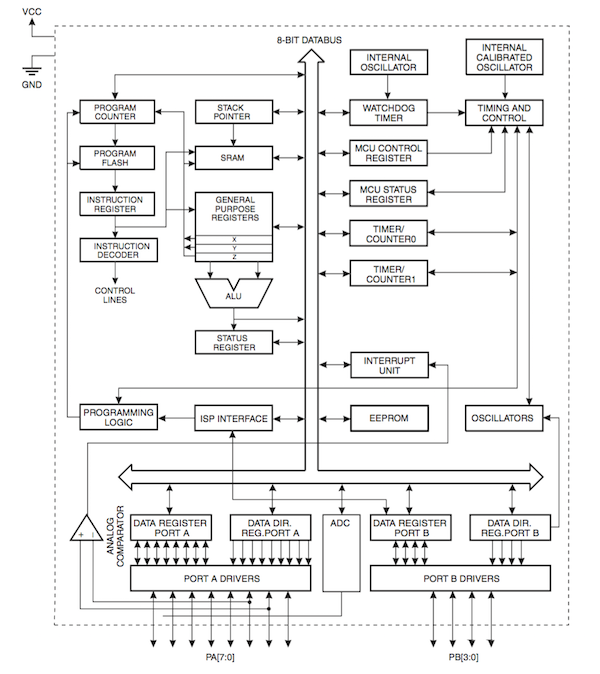
ATtiny24/44/84 is a 8-bit microcontroller based on the RISC
architecture. By executing powerful instructions in a single clock cycle, the ATtiny24/44/84
achieves throughputs approaching 1 MIPS per MHz allowing the system designer to optimize
power consumption versus processing speed
In this 32 general purpose working registers,All 32
registers are directly connected to the Arithmetic Logic Unit (ALU), allowing two independent
registers to be accessed in one single instruction executed in one clock cycle.
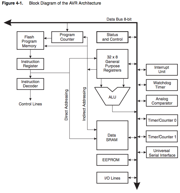
ALU –-- Arithmetic Logic Unit
The high-performance AVR ALU operates in direct connection with all the 32 general purpose
working registers. Within a single clock cycle, arithmetic operations between general purpose
registers or between a register and an immediate are executed.
Status Register---The Status Register contains information about the result of the most recently executed arithmetic
instruction.
Memories---The ATtiny24/44/84 has two main memory spaces, the Data memory and the Program memory space. In addition, the
ATtiny24/44/84 features an EEPROM Memory for data storage. All three memory spaces are linear
and regular
Watchdog Timer---
The Watchdog Timer is clocked from an On-chip Oscillator which runs at 128 kHz.
Clock system---All of the clocks
need not be active at a given time. the following is the clock subsystem
CPU Clock – clkCPU,I/O Clock – clkI/O,Flash Clock – clkFLASH,ADC Clock – clkADC
Power Management and Sleep Modes--- Idle Mode, ADC Noise Reduction Mode,Power-Down Mode,Standby Mode these are the sleep modes.
I/O--- All AVR ports have true Read-Modify-Write functionality when used as general digital I/O ports.
This means that the direction of one port pin can be changed without unintentionally changing
the direction of any other pin with the SBI and CBI instructions. The same applies when changing
drive value (if configured as output) or enabling/disabling of pull-up resistors (if configured as
input). Each output buffer has symmetrical drive characteristics with both high sink and source
capability. The pin driver is strong enough to drive LED displays directly.
8-bit Timer/Counter0 with PWM---Timer/Counter0 is a general purpose 8-bit Timer/Counter module, with two independent Output
Compare Units, and with PWM support. It allows accurate program execution timing (event management)
and wave generation.
Learning outcomes
The datasheet helps us while selecting the microcontroller and pin diagrame helpfull for setting the code. port information also get from datasheet ,so when we design any board then datasheet is usefull