Eagle design
As per the instructor lecture i know how to use the eagle and for more i use the you tube and saw some tutorials of eagle.i have to make one hello board with one led and button connected
steps for creating the ckt of my hello board
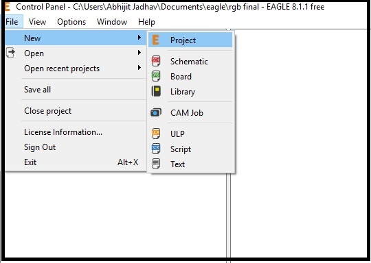
I first download the eagle from google when we install the eagle at that time it requires the email id and password.now eagle is in my laptop
Steps of hello board design
i open the eagle then i go to the file then i click on new project then i give the file or project name i.e hello board
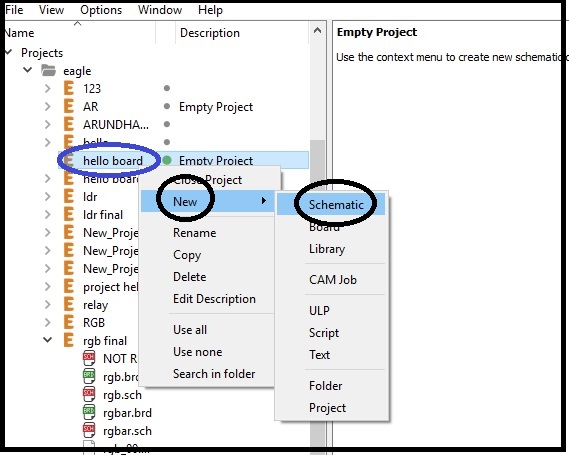
actually when we click on our project name the at right side one list open in that i have some option but for every design we first draw the schematic and then switch to the board.thats why i choose the schematic first.
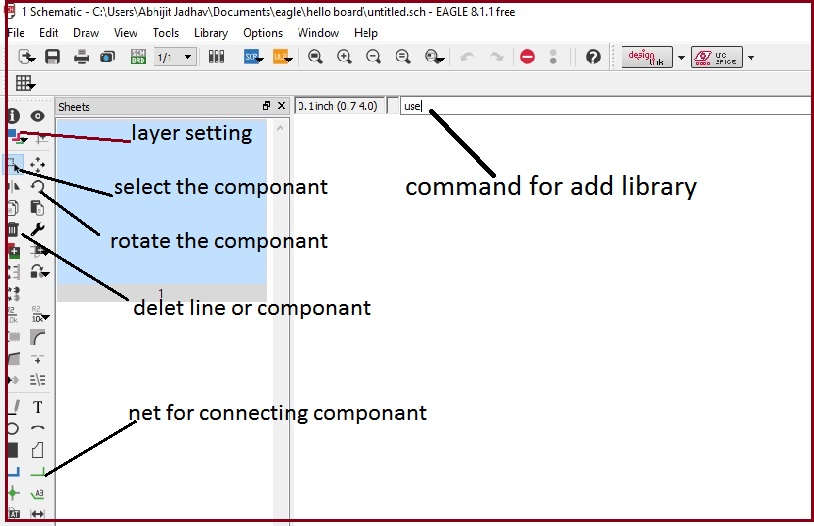
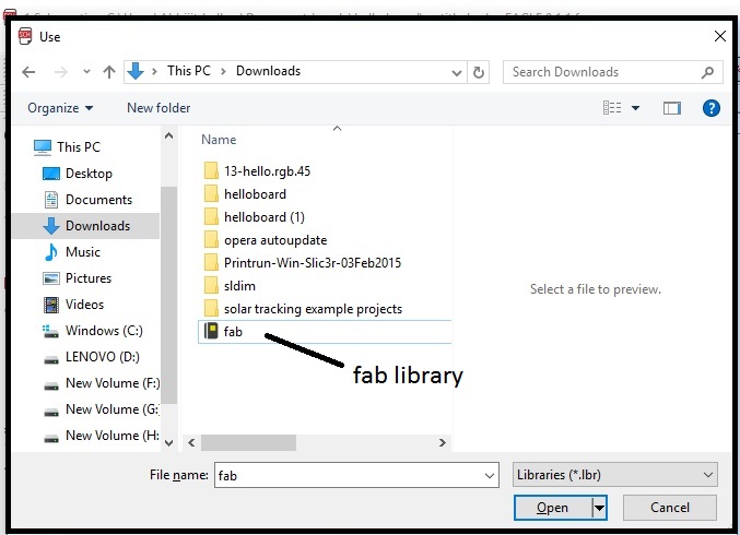
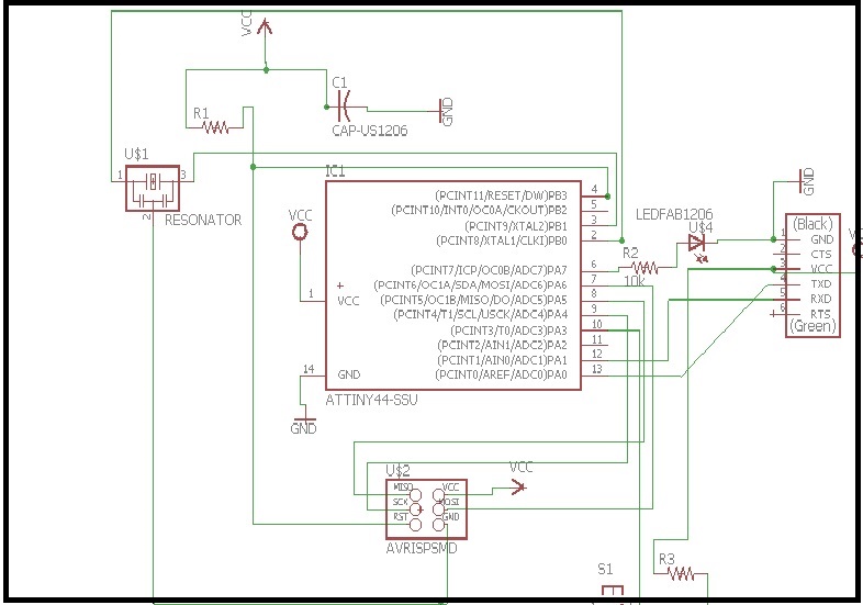
then there is one window open in that i have to create the schematic of that hello board.i call componant here and then i connect that componant to each other according with requirment.For design the hello board i requird the fab library of componant so i download the the library from fab academy website.then in schematic window in command box i type use then it goes to our download folder
then i choose fab library and say open.
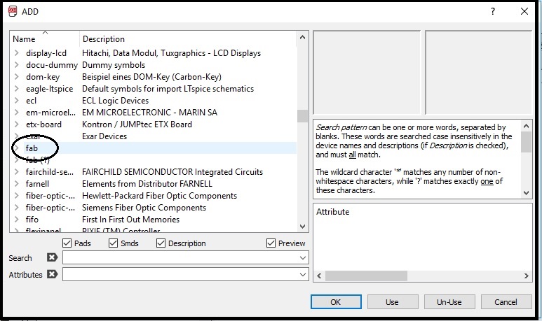
then i use command add in that command box i check fab library added or not.in that library the new fab library is added.
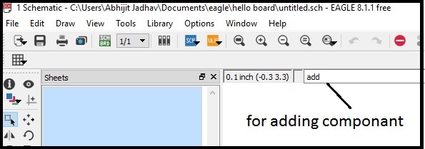
Then i type add this is for adding the hello board componant.when i type add then it moves to the library.
In this library firstly i go to the fab library then i open this library then in taht one by one i choose componant .first i choose the attiny44 from that and i put that componant on schematic window
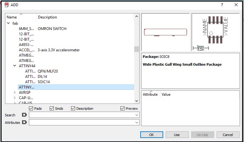
from neils hello word board i list out the componant and according with that i add the componant actualy it indicats the pading of that componant because there are some through hole componant and some of them are smd componant.
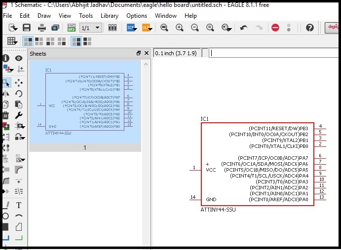
I choose all smd componant and specialy resistor and capacitor are of 1206 package list
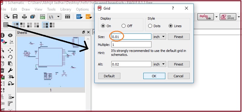
now all componants are in schematic window now its time to connect it.but when the grid is large then the componant not connected to each other in good manner it takes large space and minimum accuracy.so now i set the grid it is at the corner of window i open that grid setting window and i set the pixel size is 0.01 inch.and on the display.
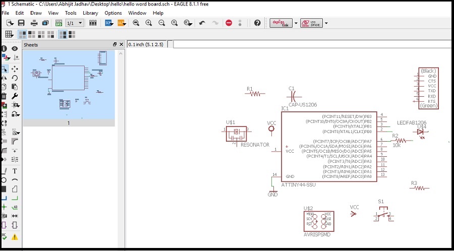
now i coonect the componant with the help of net which is having green color.
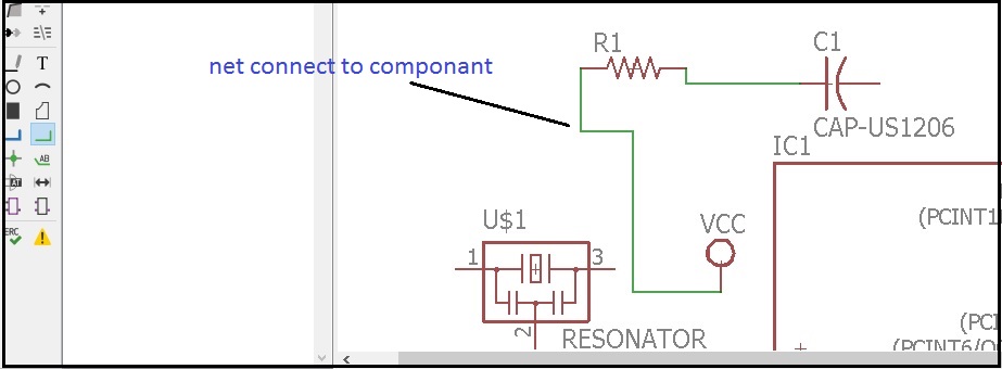
my all componants are connected to each other.in this where the ground and vcc is connected there i connect the vcc and gnd symbol,so they all connect to each other .
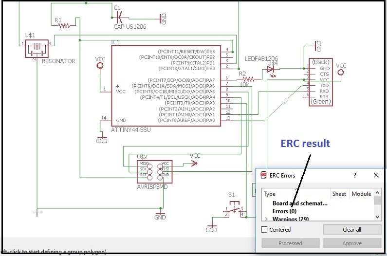
now i check the erc and it shows the zero error but i have some warrnigs,my schematic is ready to switch.
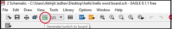
Now for creating the path of ckt i switch from schematic to board.on upper window there is one option switch to board i click on that board.
there is one new black window open in that my all componant come but they are not in that rectangle.they just switch here.
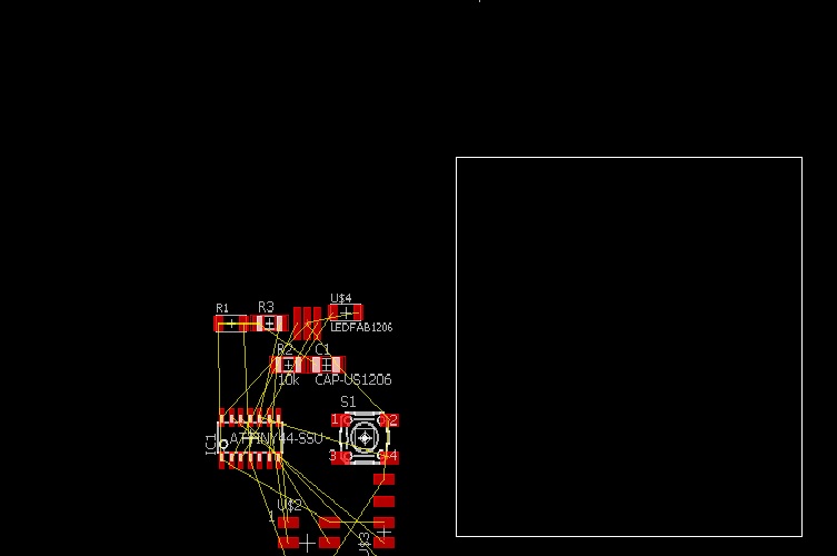
I move all componant in that rectangle
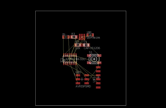
by using rotate,move ,mirror command i set the all componant
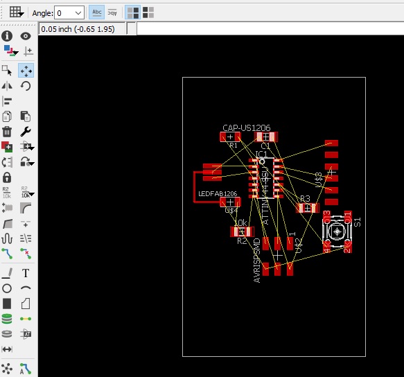
then with the help of route i coonect the all path .in this yellow line indicates that which componant connected to which componant and according with that i made path with the help of route.
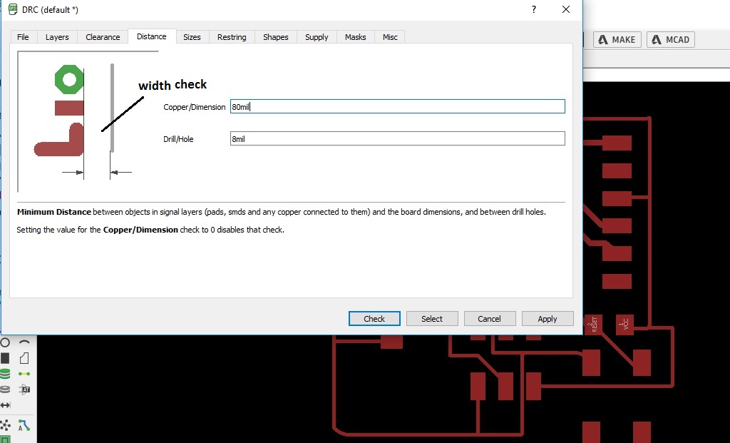
Design rule checking or check(s) (DRC) is the area of electronic design automation that determines whether the physical
layout of a particular chip layout satisfies a series of recommended parameters called design rules. (according by wikipedia)
The most basic design rules are clearance,size of pads,layer setting,width . The first are single layer rules. A width rule specifies the minimum width of any shape in the design. A spacing rule specifies the minimum distance between two adjacent objects. These rules will exist for each layer of semiconductor manufacturing process, with the lowest layers having the smallest rules and the highest metal layers having larger rules.
Now that the PCB design is reduced to the size we want to check a DRC, This checks the dimensions and the clearance of our circuit. We have to rectify the errors given here as these generally are erros related to clearance of the tracks.
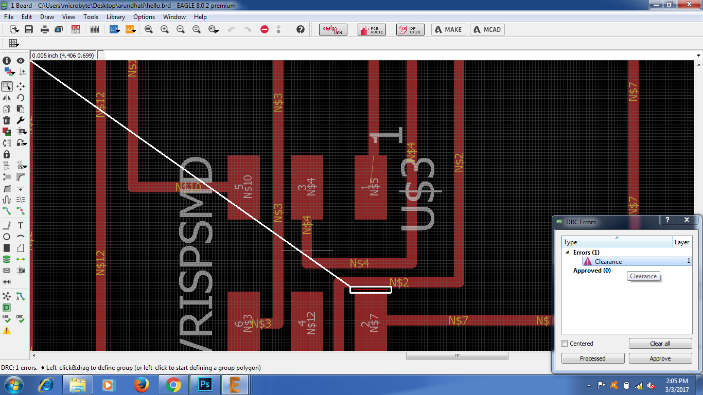
i set design rule for my board.In that i set the width ,distance between componant etc.my all board is ready in that now no any wire is overlap then i cheak the drc no error genrated.
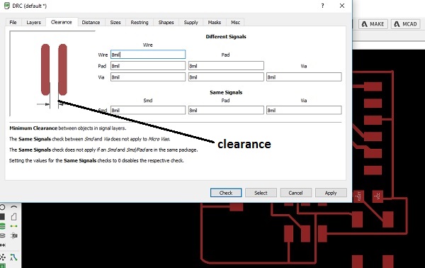
Then i again cheak the DRC and this time it is shows 0 error
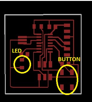
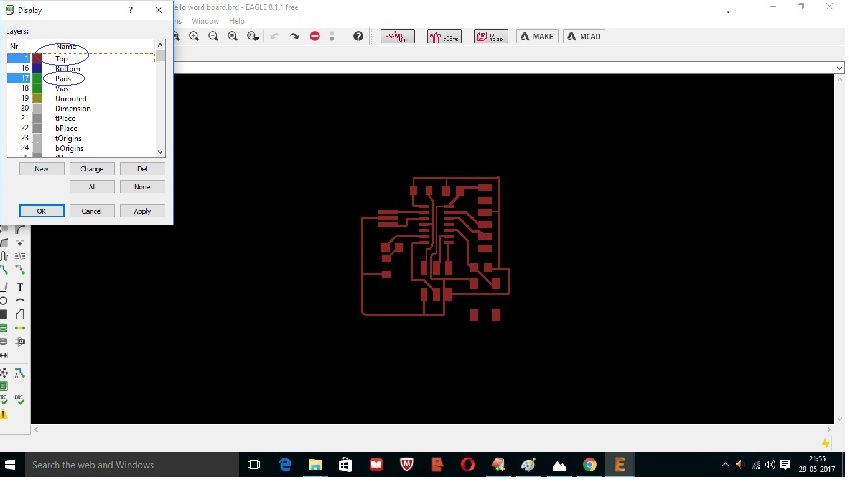
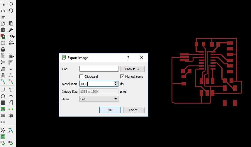
In this there are 2 part one is inner and other is border.the innere part is traces of board ,and border is for cutting.so i have to save these two parts separatly.for save the traces i open the layer setting and i off the all layers and just on the top and pads
then i go to the file and click on export then click on image.
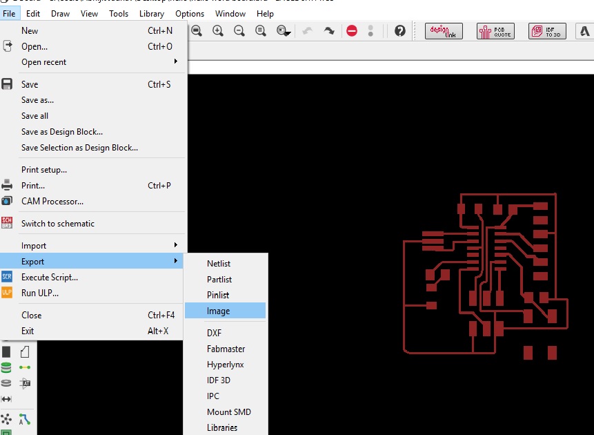
in the below fig.i set the resolution at 1000.then select the monochrome and click on browse and save that image.
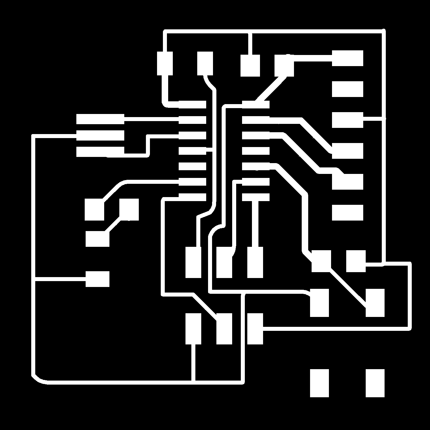
my png image looks like this in that the track is having white color.which is needed for modela machine.
I repeat the same process for the border,but in this i on the bottam and dimention and other layers i off.
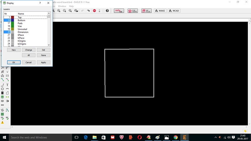
In this also i set resolution as 1000 and image as monocrome.this border is for cut the board

Learning outcomes
In my engg.i learn diptrace and orcad but this is easy software for learn for making ckt.i like this software for my final project also i design my board from this software