WEEK 15
EMBEDDED NETWORKING AND COMMUNICATIONS
ASSIGNMENT
- Design and build a wired &/or wireless network connecting at least two processors
Preperation
The goal of this week is to communicate between the microcontrollers. This week i learned the basics of different communication protocols and decided to build and control multiple mcu's using I2C protocol. This was the one of the toughest week for me , maximum efforts i had taken this week to complete this assignment.
Embedded Communication
Embedded communication means transport of information from one circuit to another circuit. Where the circuit which transmits the data is called Transmitter and the circuit who receive the data is called Receiver. Atleast one Transmitter and a Receiver is required to establish the communication. Communication may be in one direction or in both directions, there are different classifications according to this, basic classification is Synchronous and Asynchronous communication. If breifing about this in one sentence, Synchronous means: sender and receiver use the same clock signal and Asynchronous Means: sender provides a synchronization signal to the receiver before starting the transfer of each message.
Communication Protocols
A communication protocol is a system of rules that allow two or more entities of the communications system to transmit information via any kind of variation of a physical quantity. Communications protocols cover authentication, error detection and correction, and signaling. They can also describe the syntax, semantics, and synchronization of analog and digital communications. Communications protocols are implemented in hardware and software. There are thousands of communications protocols that are used everywhere in analog and digital communications.
Communications devices have to agree on many physical aspects of the data to be exchanged before successful transmission can take place. Rules defining transmissions are called protocols. There are two main categories in this.
Inter System Protocol
- UART Protocol
- USART Protocol
- USB Protocol
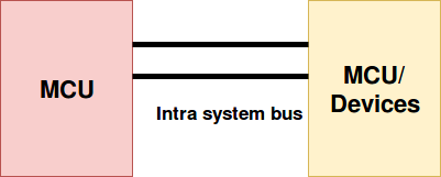
Intra System Protocol
- I2C Protocol
- SPI Protocol
- CAN Protocol
This is used to communicate between two different devices like a communication between a computer and microcontroller. It uses a dedicated bus to communication.

Different Inter system protocol:
This is used to communicate two devices within the circuit. The circuit complexity, powerconsumption will be less in this.
Different Intra system protocol:
I shared the above information here for getting and idea about the communication protocols which i got from one of the link , while searching about the protocols, If any one wanted to learn more they can check the above link. I selected to implement I2C protocol communication between atleast two processors. Here i will breif about the protocol as a quick reference.
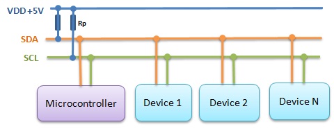
Inter integrated Circuit (I2C) Protocol
I2C is a serial protocol for two-wire interface to connect low-speed devices like microcontrollers, EEPROMs, A/D and D/A converters, I/O interfaces and other similar peripherals in embedded systems. It was invented by Philips and now it is used by almost all major IC manufacturers. There are a lot of documentations and tutorials are available in internet regarding this topic. one of the usefull documentation i refered is I2C BUS. The bus configuration of I2C communication is shown below.
Bridge Board
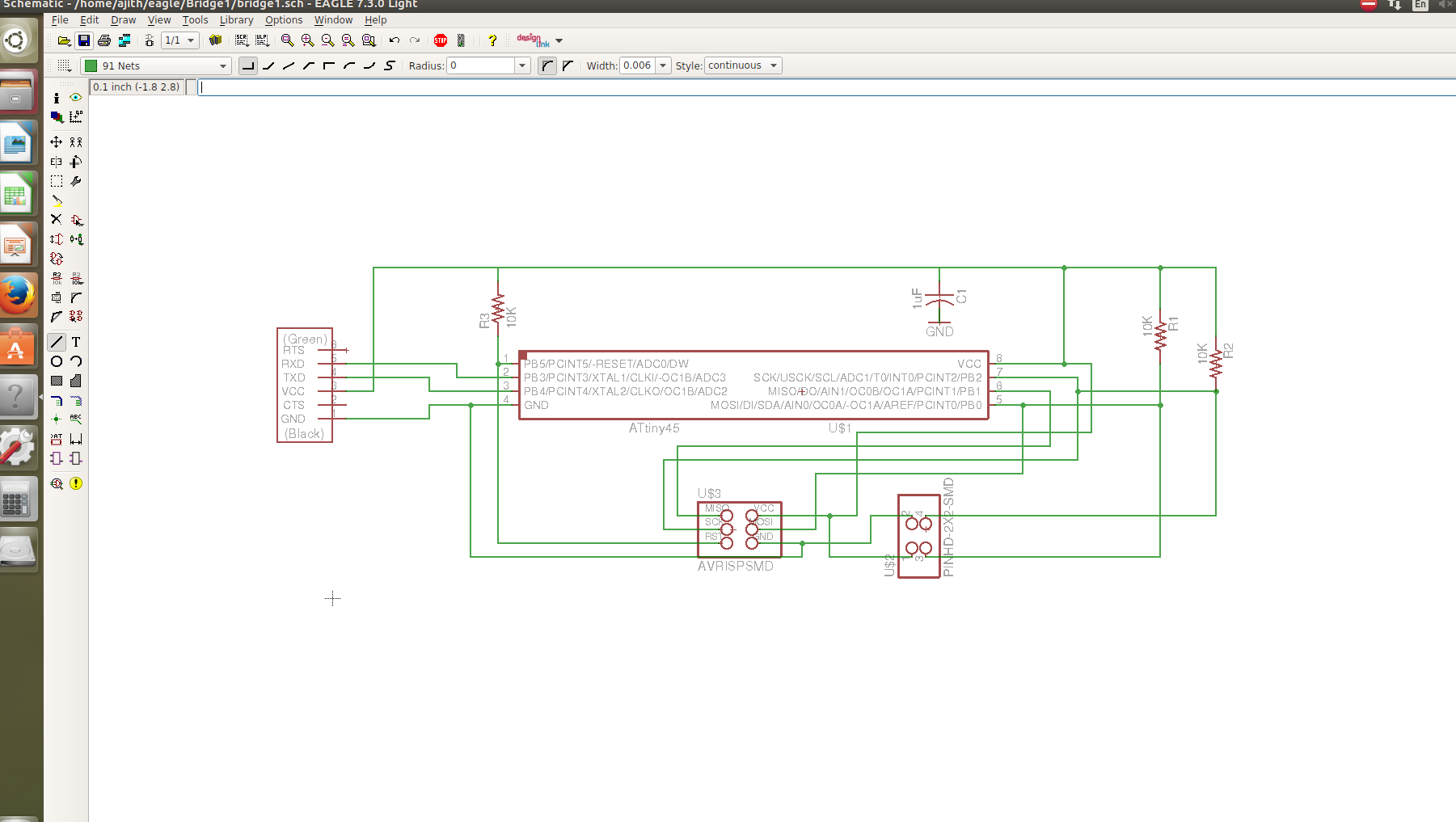
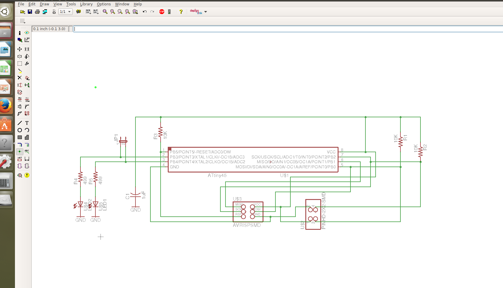
After going through several documentation about i2c protocol implementation, i palnned to contol two node microcontroller boards with a bridge board. I followed neil's schematic and started design of schematic in eagle cad software. You can refer my previous electronics weekly assignments on how to draw the schematics in eagle. This is a Attiny45 based board where i2c and ftdi interfaces are taken. The image shown below are my bridge board schematic diagram.
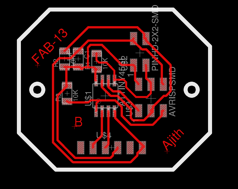
After completing the schematic, routing of the tracks were done and finally the files were exported into png files required for milling with modela cnc. In this i have given label "B" to identify it as a Bridge, My bridge board layout is shown below.
Node Board
Next is to design of node board, for this also i followed neil's node schematic. It is also attiny45 based board with i2c inerface. Additionally i added provision to add two leds to the empty ports PB2 & PB3, same pins were terminated in two jumpers for connecting devices directly to the board. Below showed images are the schematic and position diagram of my node board.
In the node board, i have given the label "N" to identify it as a node. Finally the board files were exported after routing in png format.

Making Bridge and Node in Modela
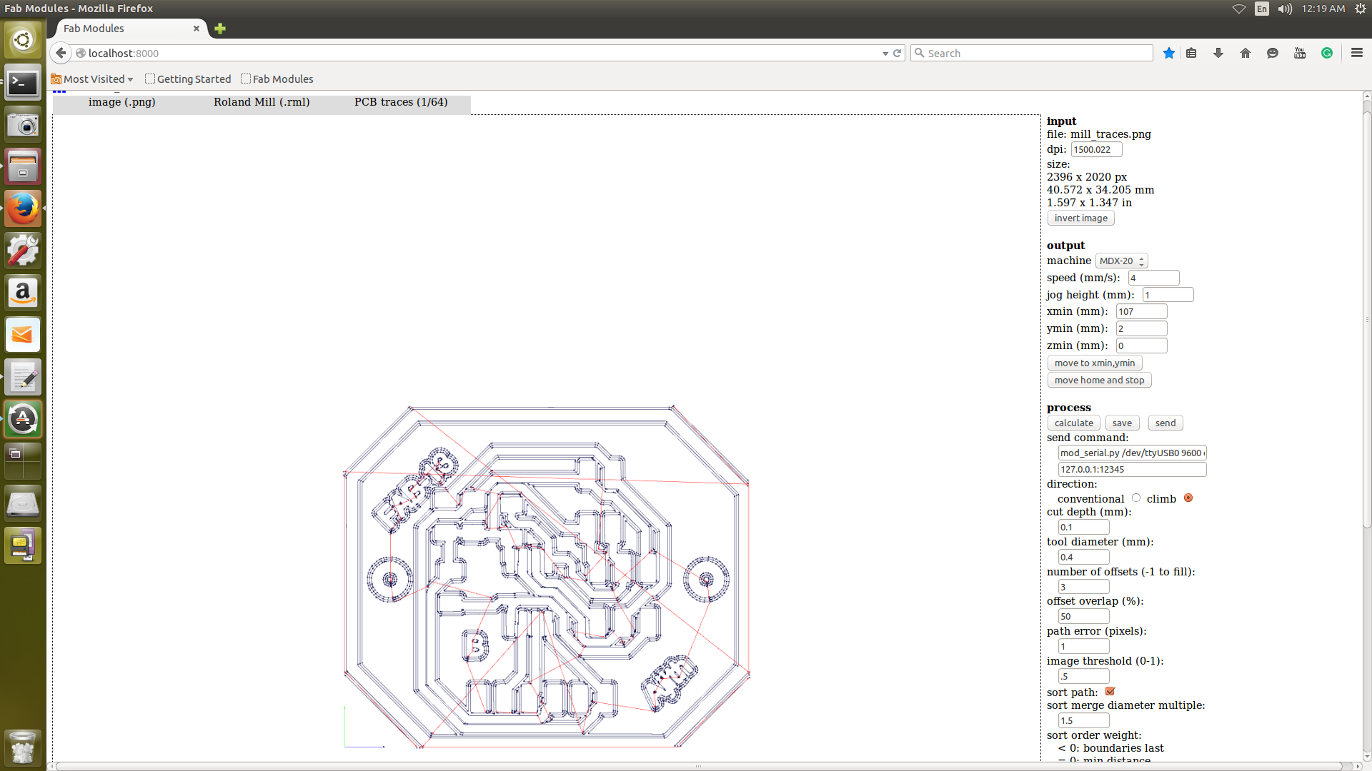
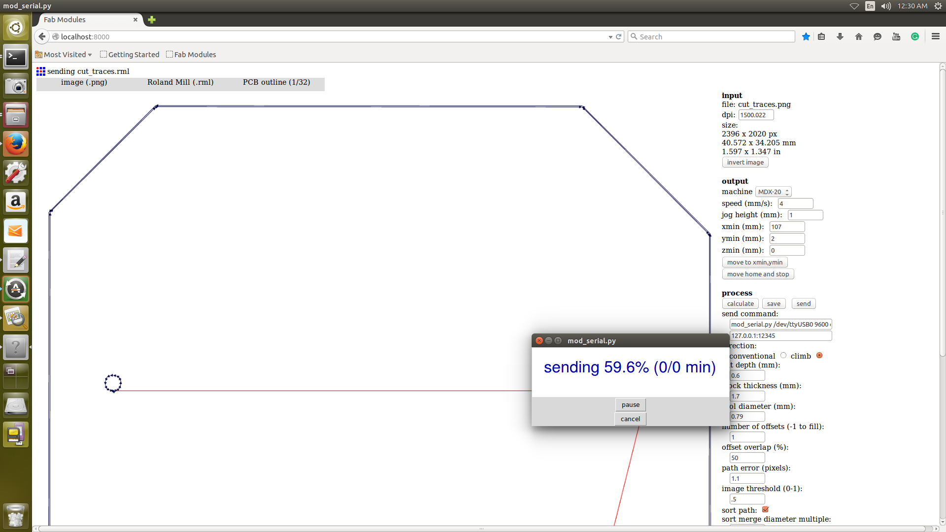
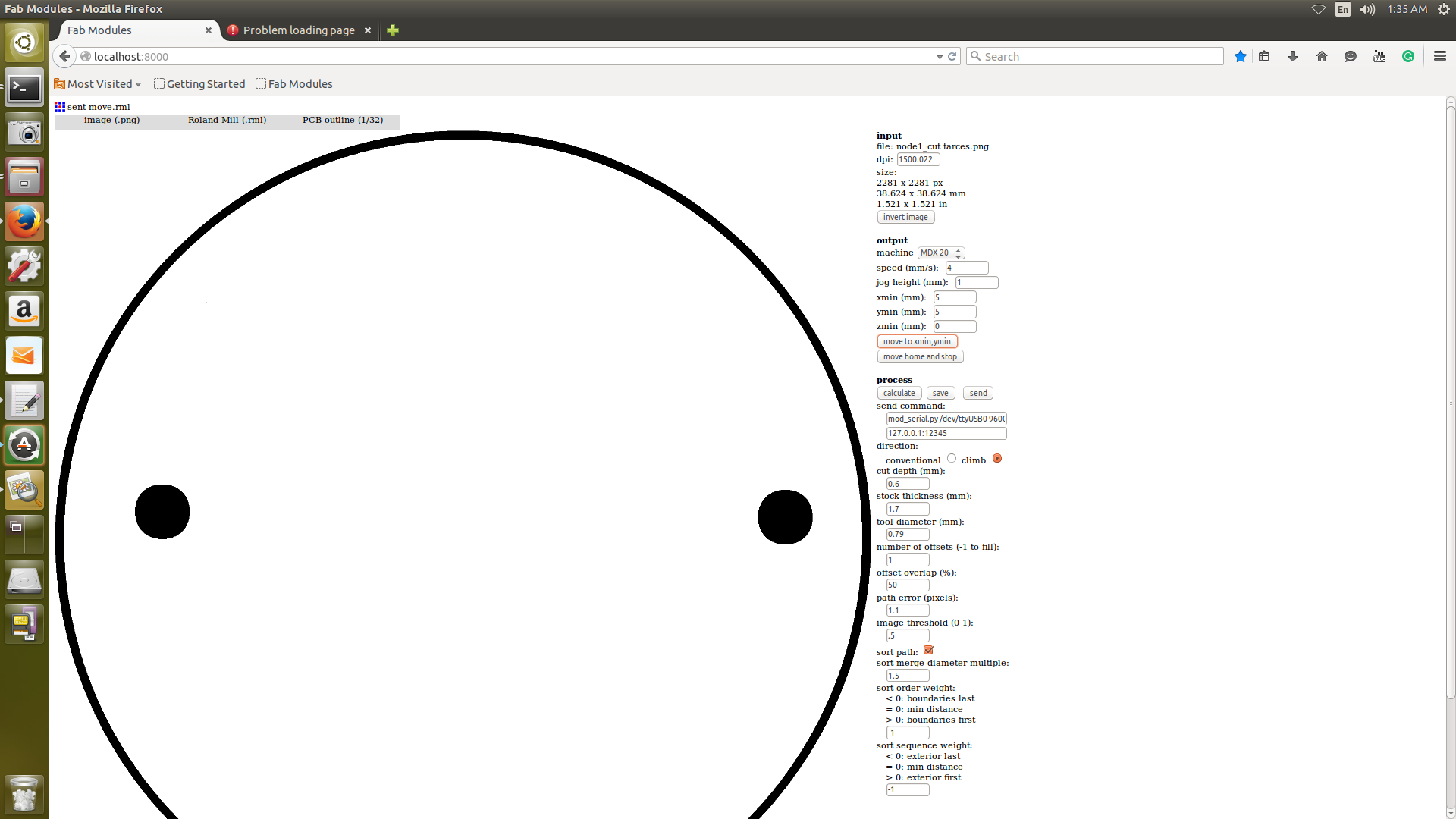
The files were ready for milling, the machine were set like i did in the previous weeks. First i started with bridge board, this week i used fabhtml-locally installed version to control modela. Used 1/64mm(0.4mm) bit for milling and 1/32(0.8mm) bit for cutting the board.
Bridge board Milling traces and cutout settings
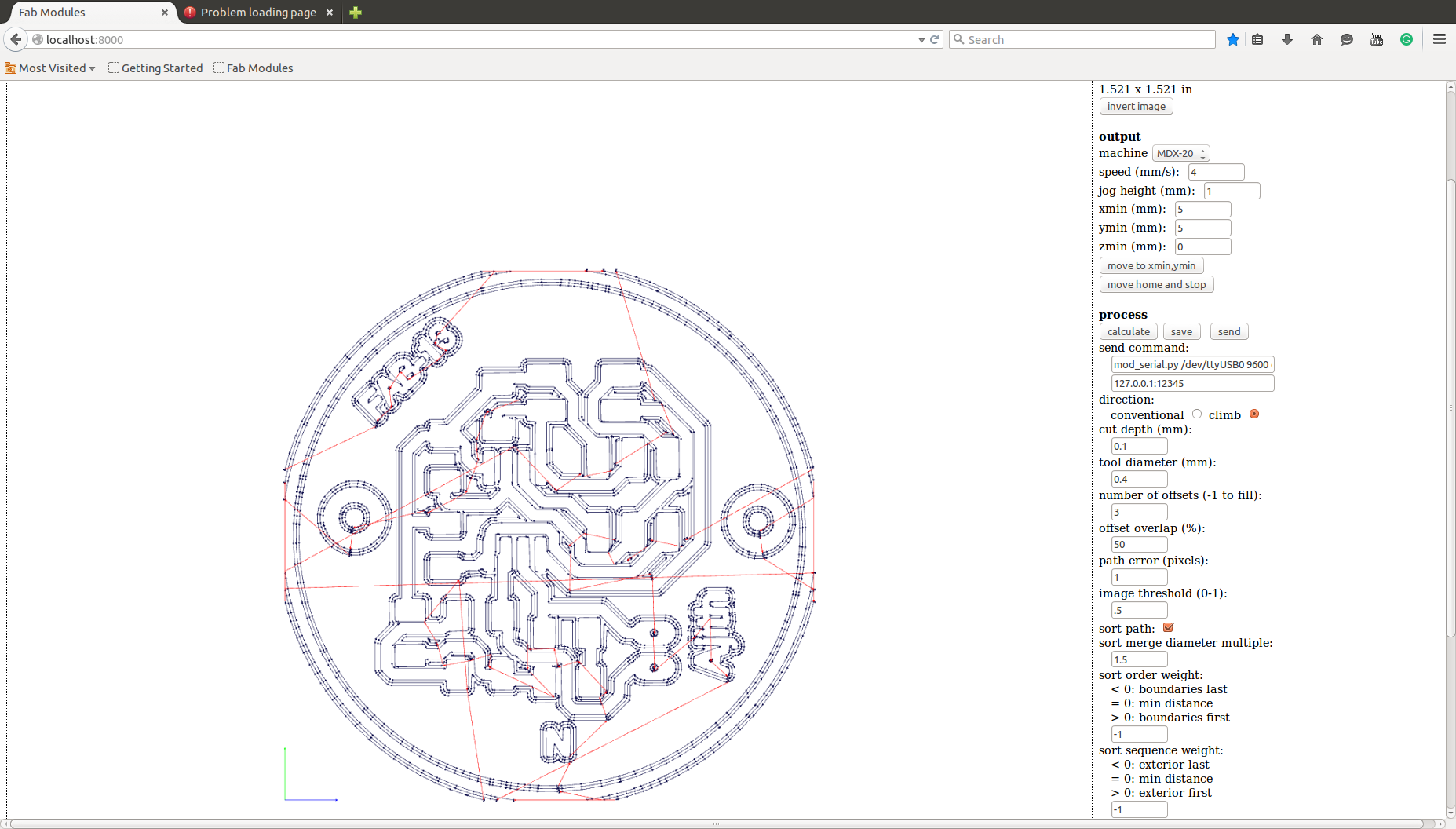
Node board Milling traces and cutout settings
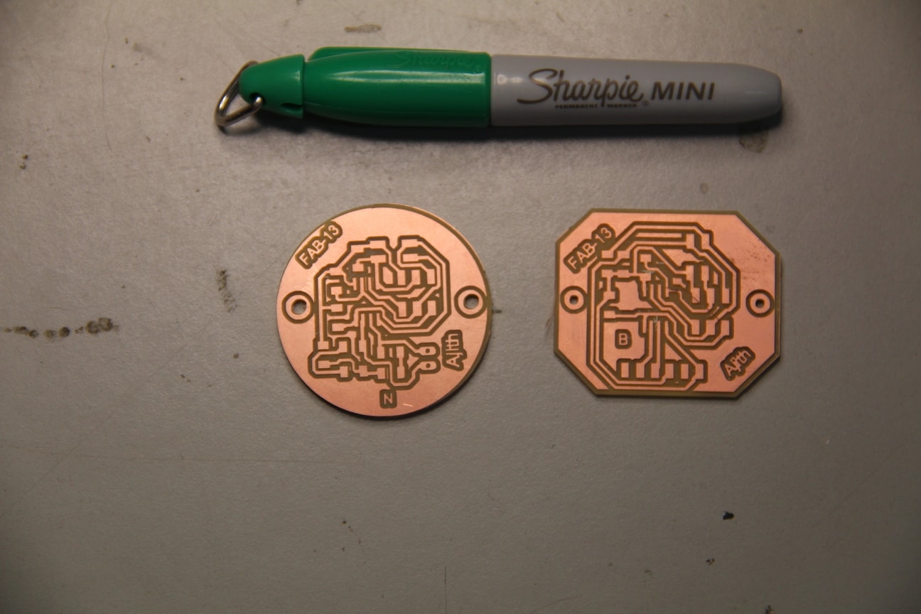
It take aroung 30 minutes to make these two boards in modela. The milled board is shown in the below image. You can clearly identify which is node and which is bridge in this.
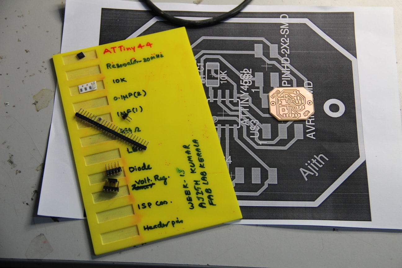
Compnenet placement
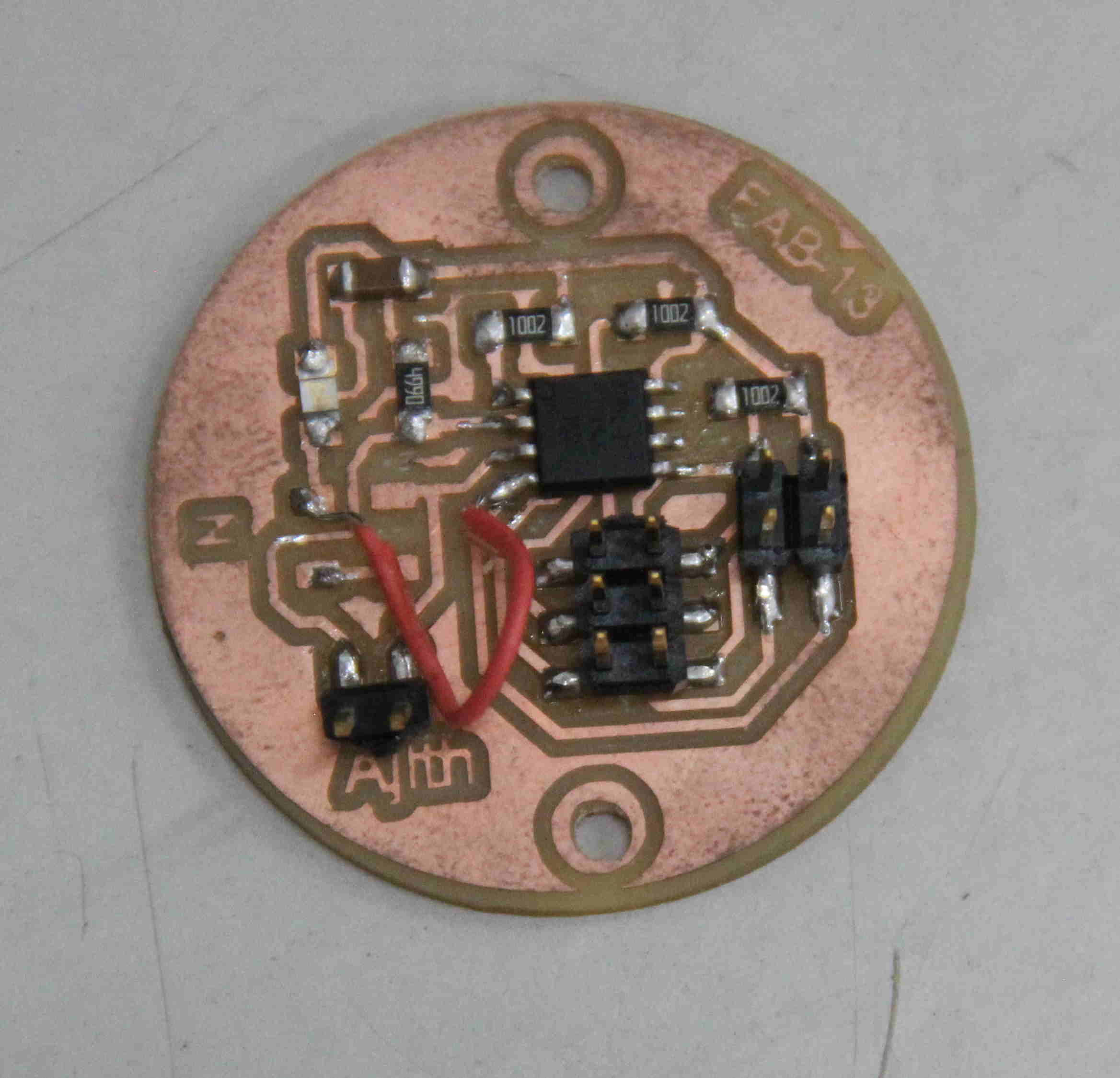
Now my pcb are ready for soldering, collected componenets from fab inventory and arranged with the position diagram of each. Soldered all componenets as per the position diagram. It contains only a few componenets won't take too much time, this was the easiest part for me.

All the componenets were soldered except the LEDs and resistor at the port PB2 & PB3. The below showed image is the hero shot of my Bridge and Node board after soldering.

Issues faced
Actually in my node board there was a small mistake happened the groung point of the LED cathode is not connected in the layout, i didn't noticed that after soldering and while testig only i found this. Then i used a wire jumper to connect the cathode point of LED to GND point of Attiny45 as shown below.
I2C Programming
After going through some of the documentation i understand that implementation of the protocol is little bit toughest part. Gone through several documentations and understood the basics, first i thought to implement the programming part in C language, later i thought to start with adruino and after understanding it will come back to c progarmming otherwise it will be difficult for a beginner. First i used arduino as bridge and using wire.h we can implement i2c, given two slave address 2 for node1 and 3 for node 2. Here arduino will act as the master and it will call the two slaves (i.e node1(add:3) & node2(add;3)).
Arduino Uno program
//Code for the Arduino Uno
#include < Wire.h>

void setup()
{
  Wire.begin(); // join i2c bus (address optional for master)
}

byte x = 0;
byte x1 = 0;
void loop() {
  Wire.beginTransmission(0x2);
  Wire.write(++x % 2);
  Wire.endTransmission();

  delay(1000);
    Wire.beginTransmission(0x3);
  Wire.write(++x1 % 2);
  Wire.endTransmission();

  delay(1000);
}
The below showed programs needs TinyWireS.h library inorder to run the programs in tiny category of microcontrollers. You can get it from this link. Download it, unzip it and save it to the arduino library folder. Next for each node i had made the program as shown below. i had taken renjith's node as node 2 , Both the programs were fused into the node boards using my fab ISP through arduino ide.
Node 1 program
#define output(directions, pin) (directions |= (1 << pin)) // set port direction for output
#define input(directions, pin) (directions &= (~(1 << pin))) // set port direction for input
#define set(port, pin) (port |= (1 << pin)) // set port pin
#define clear(port, pin) (port &= (~(1 << pin))) // clear port pin

#define LED_PIN PB3

#define I2C_SLAVE_ADDRESS 0x2 // Address of the slave 2

#include < TinyWireS.h>

void setup()
{
    output(DDRB, LED_PIN);
    clear(PORTB, LED_PIN);

    TinyWireS.begin(I2C_SLAVE_ADDRESS); // join i2c network
}

void loop()
{
  byte recd = 1;
  if(TinyWireS.available()) {
      recd = TinyWireS.receive();
      if(recd == 1) {
          clear(PORTB, LED_PIN);
      } else {
          set(PORTB, LED_PIN);
      }
  }
}
Node 2 program
#define output(directions, pin) (directions |= (1 << pin)) // set port direction for output
#define input(directions, pin) (directions &= (~(1 << pin))) // set port direction for input
#define set(port, pin) (port |= (1 << pin)) // set port pin
#define clear(port, pin) (port &= (~(1 << pin))) // clear port pin

#define LED_PIN PB3

#define I2C_SLAVE_ADDRESS 0x3 // Address of the slave 3

#include < TinyWireS.h>

void setup()
{
    output(DDRB, LED_PIN);
    clear(PORTB, LED_PIN);

    TinyWireS.begin(I2C_SLAVE_ADDRESS); // join i2c network
}

void loop()
{
  byte recd = 1;
  if(TinyWireS.available()) {
      recd = TinyWireS.receive();
      if(recd == 1) {
          clear(PORTB, LED_PIN);
      } else {
          set(PORTB, LED_PIN);
      }
  }
}
Below showed is the output of the above programs, the circuit worked correctly after a lot of debugging in code. You can see in this the arduino is sending the address each node will respond to the address and turned on the LED attached to the PB3 port, Port PB2 i kept open.
Final programming
Programming Bridge
My next plan was to replace arduino with my Bridge board, for that i searched and found to use tinywire library to program master. I changed my master program from adrunio compatiable Wire.h to TinyWireM.h library. You can see the edited code below and chaged the address of nodes to 3 and 4.
		//Code for Bridge(Attiny45)
#include < TinyWireM.h>

void setup()
{
  TinyWireM.begin(); // join i2c bus (address optional for master)
}

byte x = 0;
byte x1 = 0;
void loop() {
  TinyWireM.beginTransmission(0x4);
 TinyWireM.write(++x % 2);
 TinyWireM.endTransmission();

  delay(1000);
  TinyWireM.beginTransmission(0x3);
 TinyWireM.write(++x1 % 2);
 TinyWireM.endTransmission();

  delay(1000);
}
Programming Node1
In this only chage made from the previous program is changed the address to 4 from 1 . Used my Node board as Node 1 and the edited program is shown below. Renjith helped me to correct the errors in the programming part.
	//code for Node 1 (Attiny45)_edited by ajith

#define output(directions, pin) (directions |= (1 << pin)) // set port direction for output
#define input(directions, pin) (directions &= (~(1 << pin))) // set port direction for input
#define set(port, pin) (port |= (1 << pin)) // set port pin
#define clear(port, pin) (port &= (~(1 << pin))) // clear port pin

#define LED_PIN PB3

#define I2C_SLAVE_ADDRESS 0x4 // Address of the slave

//#include < TinyWireS.h>

void setup()
{
    output(DDRB, LED_PIN);
    clear(PORTB, LED_PIN);

    TinyWireS.begin(I2C_SLAVE_ADDRESS); // join i2c network
}

void loop()
{
  byte recd = 1;
  if(TinyWireS.available()) {
      recd = TinyWireS.receive();
      if(recd == 1) {
          clear(PORTB, LED_PIN);
      } else {
          set(PORTB, LED_PIN);
      }
  }
}
Programming Node2
Initially i used renjiths node as the second node, i thought to interface my elctronics production week board as node 2. The board was actually attiny44 based board and it is having different pin configurations. But SDA & SCL pins were available at the ISP connector. One LED was there in the PA7 port so programm made accordingly to blink the LED.
//code for node2-(Attiny44)_edited by ajith


#define LED_PIN 7

#define I2C_SLAVE_ADDRESS 0x3 // Address of the slave

#include< TinyWireS.h>
#include < avr/io.h>
#include < util/delay.h>

void setup()
{
   pinMode(LED_PIN, OUTPUT);

  TinyWireS.begin(I2C_SLAVE_ADDRESS); // join i2c network
}

void loop()
{
  byte recd = 1;
  if(TinyWireS.available()) {
     recd = TinyWireS.receive();
     if(recd == 1) {
         digitalWrite(LED_PIN, HIGH);
         delay(1000);
     } else {
     digitalWrite(LED_PIN, LOW);
         delay(1000);
     }
 }
}
Testing
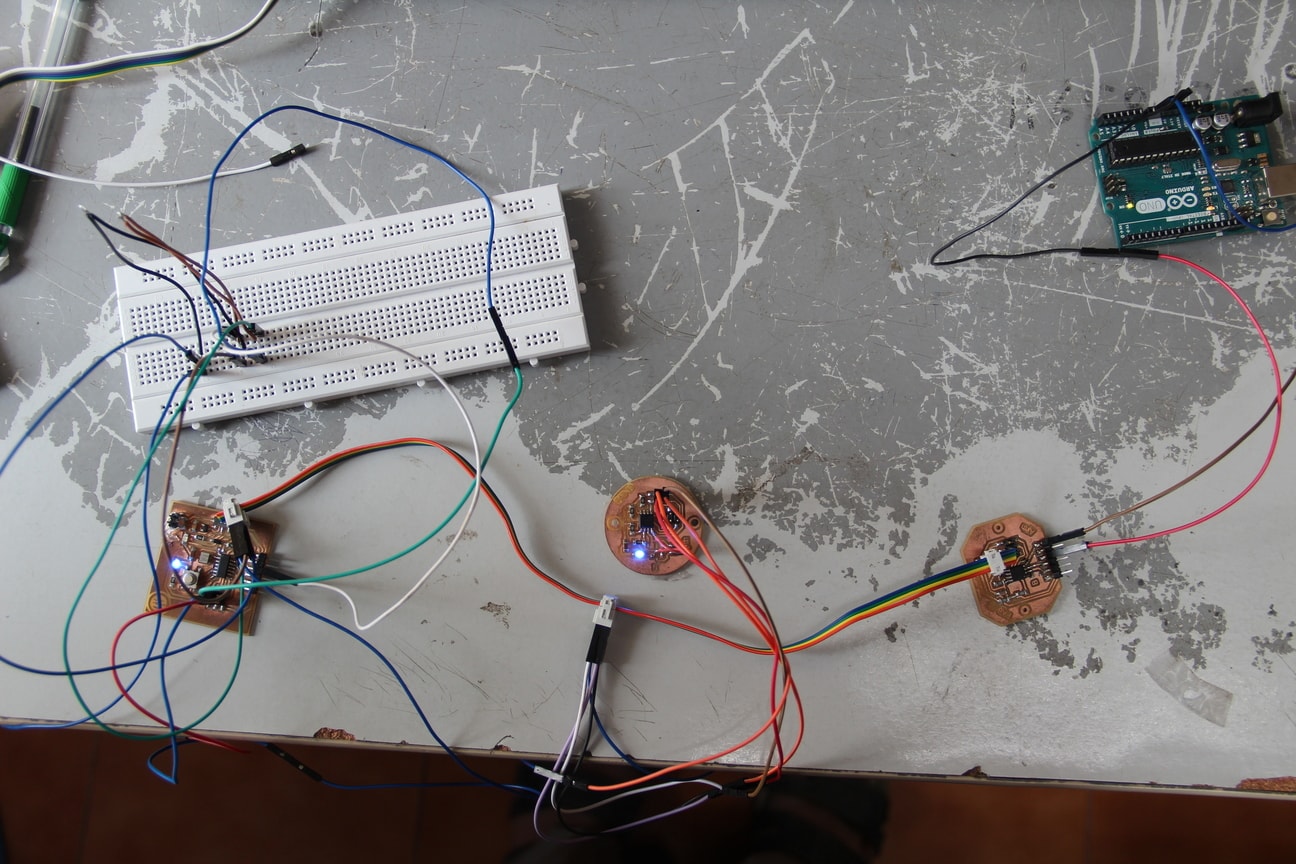
First we have to make a i2c bus cable for that we can use female 2X2 headers and ribbon cable. The connections going to the master and slaves are only 4 signals. VCC,GND,SDA & SCL connect the cable to each node. I made a small mistake in my design , the orientation of my 2X2 I2C interface connection was different in the node and master so i used jumper wires to connect from the I2C bus. All the connections were made and powered from USB through Fab ISP and it didn't worked, so i taken the 5V power from the arduino to power all the circuits. Taken two jumper wires and connected 5V and GND pin of arduino. A lot of trouble shooting i made to complete the circuit that i forgot to take snapshots. Finally my nodes started working. The entire setup is shown below. you can see the two LED's in the nodes are glowing.
Next i moved to the test bench in our lab to analyse the output in oscilloscope. I made the entire setup very neatly , routed the cables correctly and labeled the nodes and bridge the entire final setup is shown below. Power supply set to 5V and current limited to 100mA and powered on the supply and it worked and taken 20mA current from 5V supply.
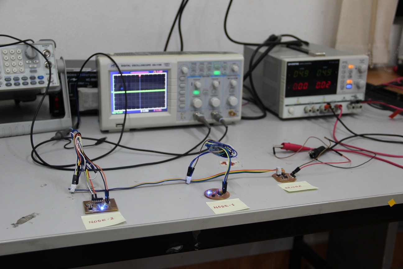
The output of the two nodes is obseved on DSO,which is shown below. In that the green one is the Node 2 output and Yellow is the Node 1 output.

Hero shot of this week assignment is shown below, the final setup of my bridge and nodes. The working video is also given below

Working Video of Bridge and Nodes(Youtube Video)