ASSIGNMENT 6.
Electronics design.
GENERAL IDEAS TO START THE THING!
I'm still new in electronics. Even if i had a succesful approach in the assignment 4, i'm still a dummy.
But for some reason I felt comfortble with the tasks. I discovered I was pretty handy with soldering, and this week's assignment also included some software exploration.
Practicing with milling is also a push, so I was quite happy to start with the thing.
SOFTWARE APROACH
I wanted to explore both of the suggested programs, but I had some problems with export options from Eagle and I decided to concentrate in solving that issue tryibng to understand "why". So my priority changed and I still need to get some time to try KiCad KiCad . Of course I used a lot the tutorials, because finding yourself in this "new" world, needs some extra help. So first, I´ve red the tutorials and even if I didn't go that deep into electronics, I started to understand a bit how the architecture of the PCB boards work.READING THE TUTORIALS AND DESIGNING THE CIRCUITS.
I started reading some Sparkfun tutorials to understand some concepts. Some of them I already had knew, but not that deep. I used this source as a reference, but I red the tutorial of the assignment and I started pretty early with the architectural part.
A I started with Eagle, I dowloaded the the FAB library directly to my computer and I installed it on the library folder of the software.I also started to wander a bit around the different windows of the program. Layers window on the image, and libraries on the left bottom.
The area on the right on the previous image is where you will include the different components needed to get your circuit working. And the final aspect is something like this.
This is the schematic view of the circuit. I took this picture as a reference for the next steps. It was easy to have it in the phone, unless you have plenty of space in the soldering desk. Once you recognise the symbols, is not that complex to read it.
You can see perfectly the correspondence between this one and the one in the previous image with the electronic codes attached.
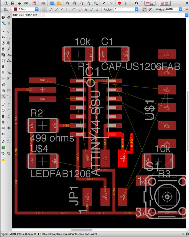
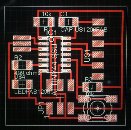
Once you're finished connecting your componentes, you switch to board view, that renders more realistic symbold of the parts you will combine in the board.
The yellow lines show the "paths" you will have to add to connect the little components; you follow them as the main refrence to clear the thing up.
At the starting point, ALL of them will be in a chaotic position, so it will take some time to arrange them and getting them organised to optimized the paths.As it was my first board, I followed the previos reference and didn't spend time on aesthetics. The second one will have more personalised items.
Then you have to start designing the paths and clearing the yellow lines off the image. Remember that you can draw paths to connect several components on a common line. No need to do individual connections. GROUP them.
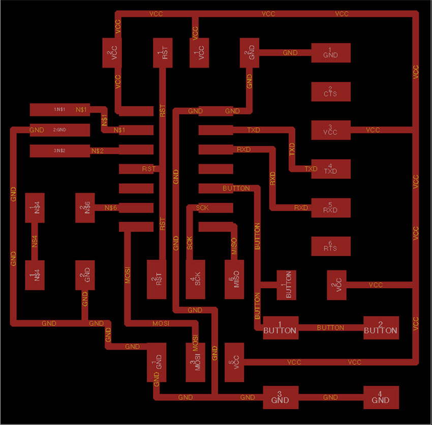
Final aspect of the board without the symbols of the components, but with the info on screen.
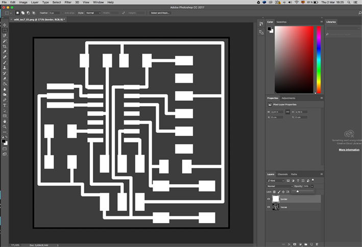
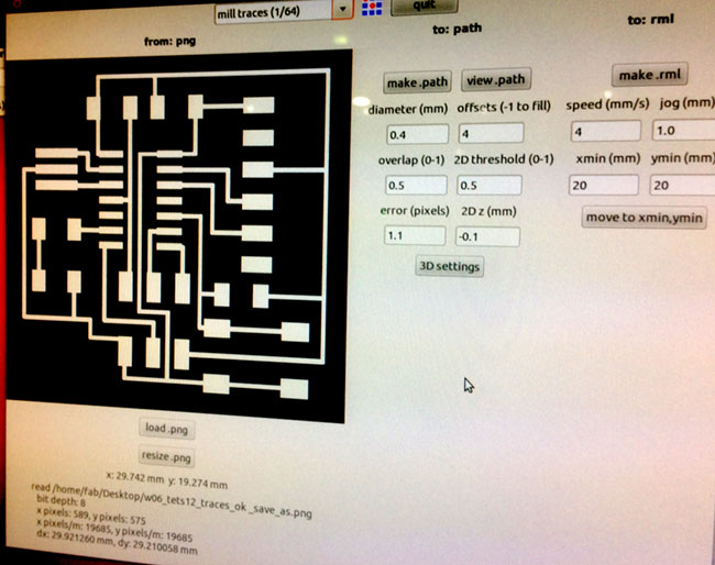
Considering that you have to trace and cut the circuit, I exported a .PNG file from Eagle, and I resized the canvas of the image to contain the edge to use as the cutting path. So you need to add 1mm in every side.
Remember to use the same size for both images (traces and cut) so they share de same 0,0 point to start milling.
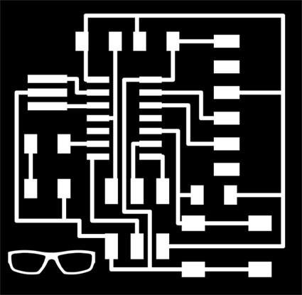
So far, i decided personalise a bit the board, but that was not a priority at all.
At this moment I was not aware of the export problems on Eagle/MacOS. My life with the board was easy so far.
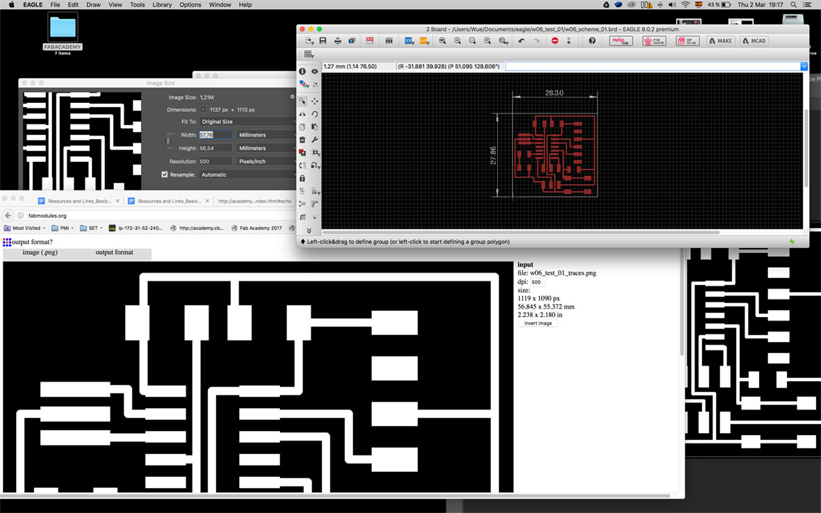
When I checked on the FabModules, I realised I had lost the size of the board, and I tried to find where the problem adding some dimensions on Eagle as references.
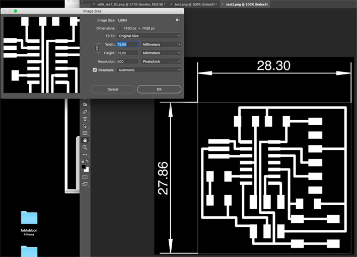
We were quite a long time trying to discover the problem and in every test we got this distrorion, sometimes following a pattern, sometimes not following any rational cause. It was a chaos and I started to get a bit disappointed with what I expected to be a very precise and intuitive program.
You can check the chaos in the values on the different interfaces.
There was some issues with the .PNG export, also in the second step, when we resize the canveas to include the path for the cutting.
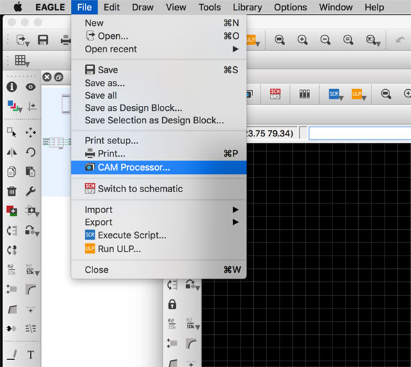
We change the protocol and started to use the cam processor way on exporting to .EPS.
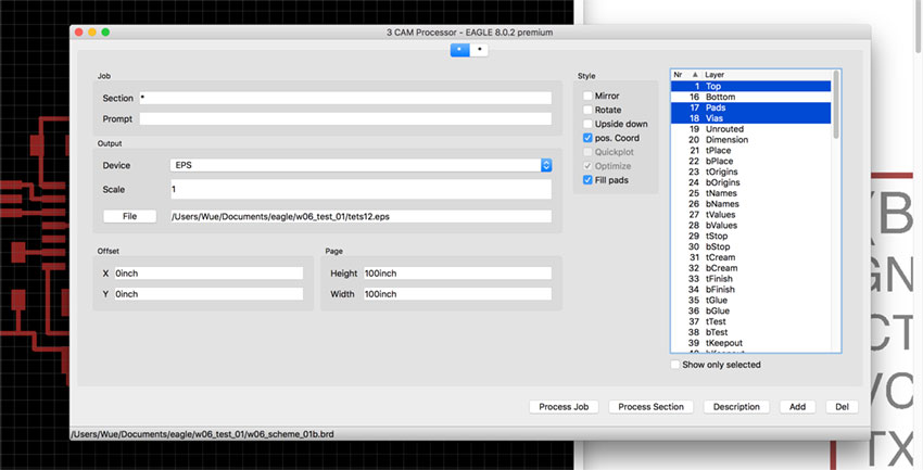
Exporting the .EPS worked fine, addind some more layers (not only the "top" one). Not a problem at all. Next step was getting the file into Photoshop or Gimp and re-start with the re-sizing of the canvas. You can checked the image before the "glasses personalised" board. I used tansparence to check that everything was in the right place.
Exporting the .EPS worked fine, addind some more layers (not only the "top" one). Not a problem at all. Next step was getting the file into Photoshop or Gimp and re-start with the re-sizing of the canvas. You can checked the image before the "glasses personalised board". I used tansparence to check that everything was in the right place.
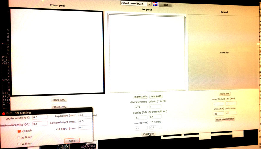
MILLING THE BOARD.
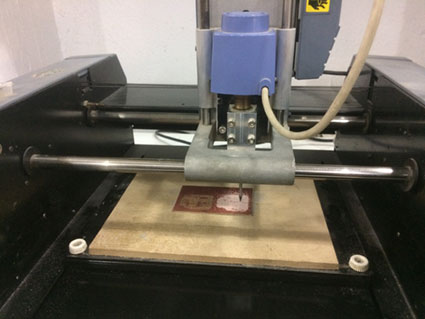
This time i wanted to try the Roland Modela MDX-20 to do it (I had already used the other Roland devices)
The interface is similar, but since It includes some extra adjustments, you can skip the FabModules process to get a similar result. Anyway I followed the same process to check the sizes of the files before I satrted with the Roland. I wanted to be sure that I got rid of the .PNG export issues.
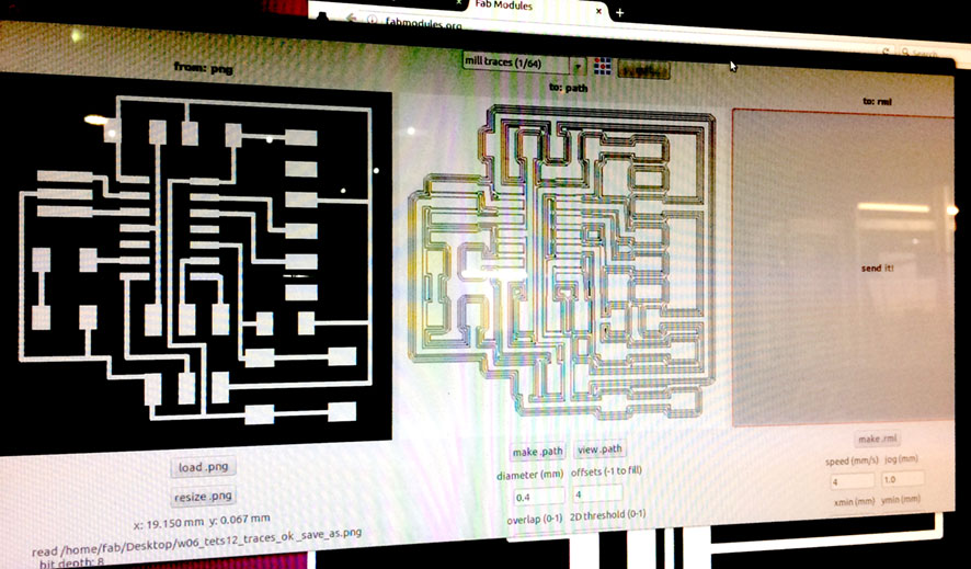
Same process ad we followed with the FabISP. First the traces and second the cut. Image shows the final levels I used to get it cut.
Here we go!
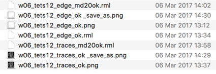
I include here all the collection of files I did to check that the ratios and sizes where correct. I'll include the in the cloud, since they actually don't add any extra information to the process. You can see the number of test I did...
The good one was the 'w06_test12_traces_ok_save_as.png'. Imagine man, what a mess.....
SOLDERING THE COMPONENTS.
Pretty confident on my recently gained soldering skills, I just wanted to take another photo of the screen to have it in my phone (a bit lazy about syncronizing the devices, this was faster)
As I said, when yu get a bit used with it, thats like a roadmap. Very helpfull on the phone.
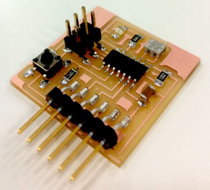
I have no photos of myself soldering, and i get very focused on the thing, so my images are very close to the final result. This time I was sure to start with the Atiny. Much easier to solder the litle crature without any interfering components around.
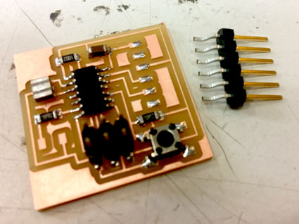
Final result. You see no "glasses" on the board, because I focused on solving the .PNG problems with the original one, no aesthetics in between me and the final result.
Well, that another good reason to have the "maps" on the phone, besides the available space in the soldering desks....hehehe

Step by Step
- Check the tools, first impression.
- Understand the logics through practice.
- When there's a problem with formats, try to solve it with some ready made tools, first.
- Don't do it directly with photoshop, that's the easy way adn you can find something more precise.
- Think twice what you're doing (get some backups!).
Method
In this assignment the method is similar to the first electronic aproach, but with some software included!
Soldering is getting better, so I didn't need to franken-hack anything.... I don't know if this is a good or a bad thing, since you don't search for alternatives. Let's see in the future.