Shown your process using words/images/screenshots.
Explained problems and how you fixed them, including how you worked with design rules for milling (DRC in EagleCad and KiCad).
Included original design files (Eagle, KiCad, Inkscape, .cad - whatever).
I chose Eagle, because it is one of the most famous, the fab libraries are available for Eagle and our Autodesk license cover it use.
First, I downloaded the free version from the webpage and installed it. Once this is done it asks your Autodesk account, so in our case it should update itself to the premium version. My case was a little different, because for some reason my registration for the free one year Autodesk license was not right. I spoke with Luciana and she fixed the problem but I had already installed the free version and done most of the redrawing process with it. I must say I haven't encounter any limitation yet. I think these came when you want to print bigger boards than 80 mm. As this was not the case, the free version worked fine, even though I am planning to reinstall it to get the full version later on.

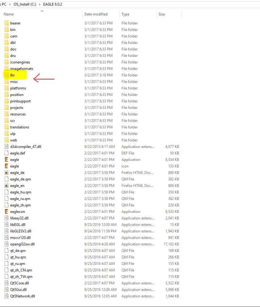
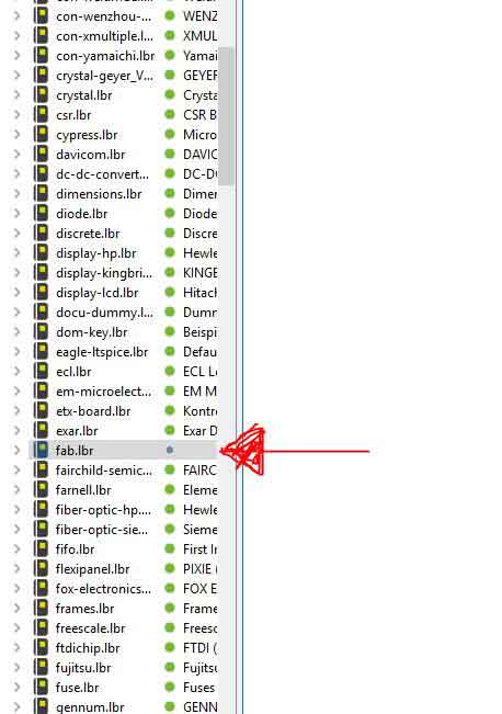
After the software is installed, I loaded the Fab libraries to it. This library contents most of the parts we will use on different Fab Academy projects. To do this, first I downloaded them from the archive. Once it is on the computer we just need to add it to the program files Eagle library folder. Once this is done the fab library will appear on the program libraries. It will appear a grey dot right next to it instead a green one as it does on the rest of the libraries. This is because it hasn't been activated yet. To do it, we just need to press on the grey circle to make green. Once the fab library is activated, it will appear on the schematics libraries to add any part we want from it.
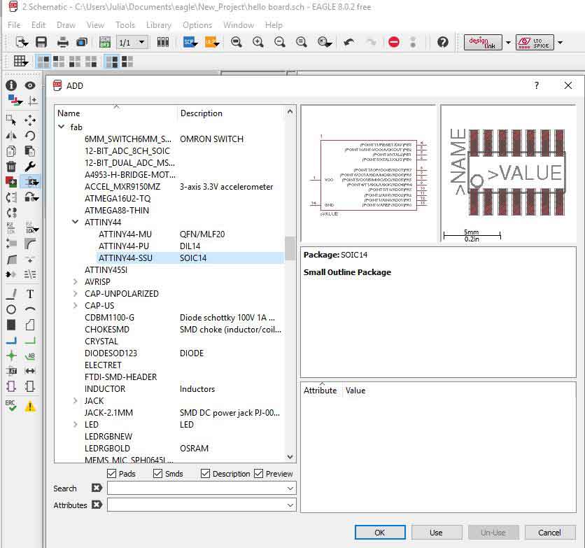
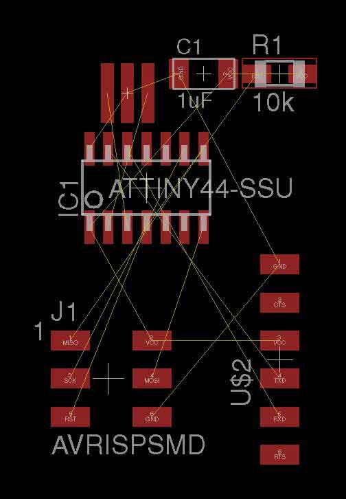
After having taken a deep look on to Neil's hello.ftdi.44 board, I wrote down all the components I was going to need. I started creating a new project in Eagle's control panel, then a new schematic. To start adding parts there is an icon on the right panel called add. Once you press it, all the libraries loaded on the program open. Eagle has a command line too, by typing add you will get to the same panel as by clicking the icon. Once the panel opens, type fab, it will lead you to the one we are interested. I pick up all the parts I needed for the hello.ftdi.44 board.
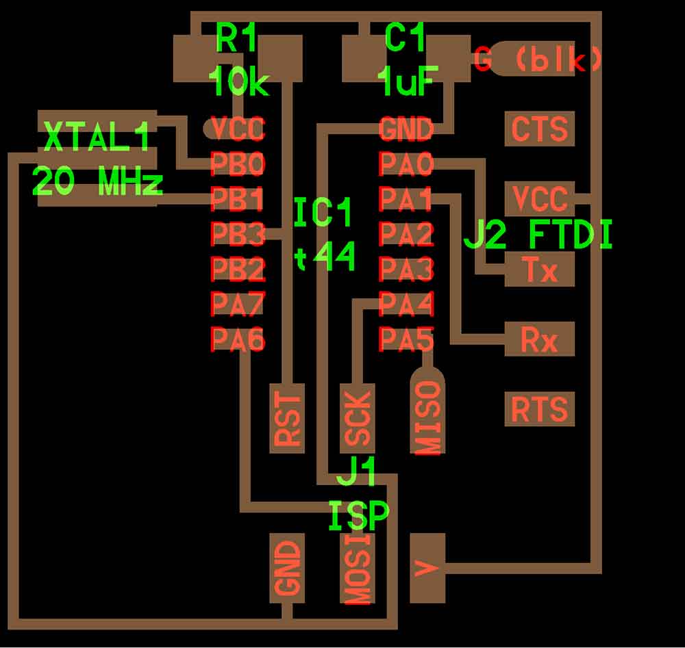
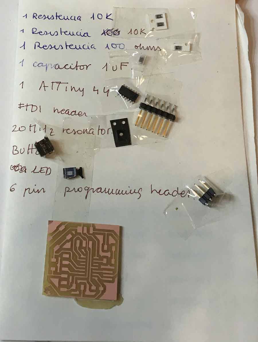
NEEDED PARTS
6-pin programming header
Attiny44A microcontroller
FTDI header
20MHz resonator
10 K ressistor
1uF capacitator
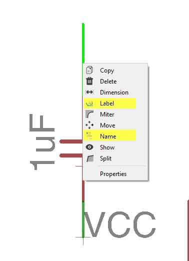
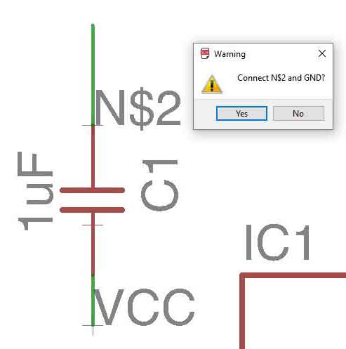
When all the parts were on the schematics, it was time to connect them. When wiring components together, it is important to remember to use the NET command, rather than the WIRE command. If you want to link two different pins or traces together but do not want to run the wiring all over the place, simply assign the same NAME to the pins. Just right click on top of the component you want to connect, a menu will appear, click on LABEL. To really connect them to another component you have to name them, right click again NAME. When there are two same names, the program will ask if you want to connect them, click ok.
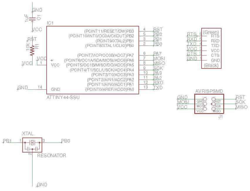
I changed the values and reference designators for the parts to match the values for the hello.ftdi.44 board.
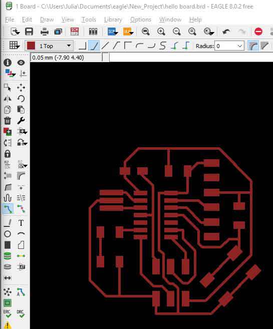
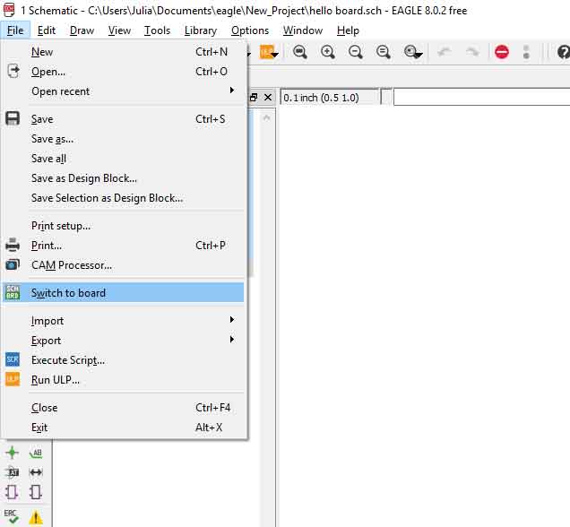
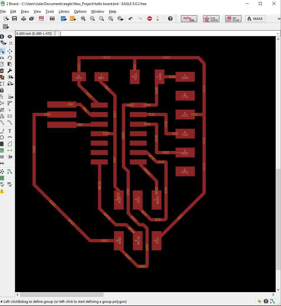
When the schematics is done, is time to move to the PCB window. To do it, you just need to go to FILE, SWITCH TO BOARD. Afterwards it will appear the PCB interface, which reminded me a little bit to Autocad’s. At the beginning, all the parts will appear on the layout without any order. There are also some thin yellow connections between the parts. This represent the connections that were made on the schematics but they are not enough, just the representation of the connections that need to be made. This will be disappearing as we route the actual connections on the PCB window. Before doing this Eagle has an Autorouting tool. (TOOLS, AUTOROUTER) but it is not very effective as it just calculates the best connection between the layed parts, it doesn’t move the parts to make it better. That is why most of the times it tends to do double sided connections. We can know if a connection is underneath because they will appear on a different color(layer) and some green circles will also appear were the connection travels from one side to the other. Once I discarded the autorouter solution I started played with the MOVE, ROTATE options to make the best layout and started connecting them with the ROUTE tool. After a bunch of tries I was finally satisfied with the final result.
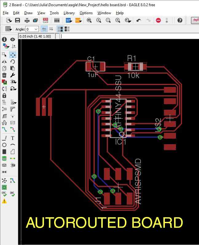
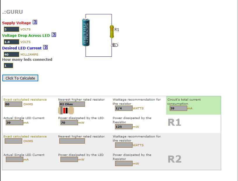
After having understand a little bit how the program worked, I decided to add the button and the led. First of all, I calculated the needed resistance for the led. It turned out to be an 82 Ohms resistance, so I chose a 100 Ohms resistance.
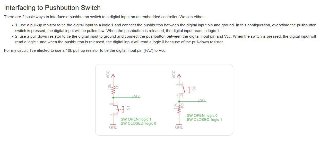
Thanks to Steven Chew's documentation from last year, I understood why is needed to add a pull-up/pull-down resistor before the button. After having connected all the elements, I arranged them on the PCB board. Once this was finally done, I checked the design rules or DRC. This will make sure that the traces are separated enough for the machine to trace them. I set up the DRC with a wire-to-wire and wire-to-pad clearance of 16 mil and a minimum trace width of 16 mil, which is easily achievable using the pcb milling machines that we have.
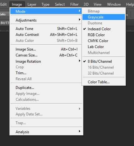
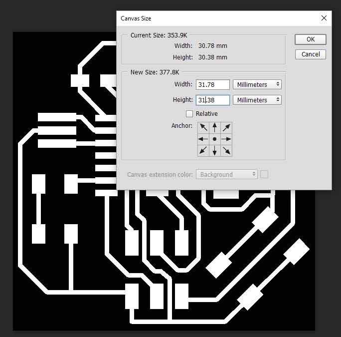
Then I Prepared the board for extracting the g-code on fab modules. First, I turned off all the layer but the top layer (traces only), which is the one I had my traces on. Then I exported the png by going to FILE, EXPORT, IMAGE. The settings have to be MONOCHROME and 500 DPI. I also exported the Dimension layer for milling the outside of the board. Once I had the png, I opened them on photoshop. It is important that the traces are in white and the rest is in black. If this is not the case, you must invert the image. Mine was alright, so I didn't have to invert it. But to make sure that the outline milling is not cutting any of our traces, is important to increase the image 1mm, which is the size of the outline trace. Eagle exports the png as an index image, first thing to edit it right is to make it a grey scale image, on IMAGE, MODE, GREY SCALE. Now we can edit it. To set the dimension and the outline right first, I convert the image to a regular layer by double clicking on top of it. Afterwards, I created a new layers, which I placed on the bottom. The I changed the canvas size, on IMAGE, CANVAS SIZE, I left the centered alignment and increased it to 1mm. I colored the bottom layer in black. The file was ready to export with the right dimension. To export the outline, I turned off the traces layer and created a 1 mm thick rectangle on the perimeter of the canva. After that was done, I had my outline traces too.
Once the png where done, I opened fabmodules app, and loaded the png doing the same settings as week 4. Once I had the g-codes I went to the Rolan SRM-20 to do the milling. I must admit, I was very nervous as last time it took me forever to mill it right. But fortunately this time the traces came out good at the first time. I changed the tool and send the outline. As the machine was running, I realized that the outline was cutting my traces! OMG!! After having checked my fabmodules setings I realized I had put for the outline 3 offsets instead of 1, so the machine was overlapping towards the inside of the board, cutting some of the outside traces... :(
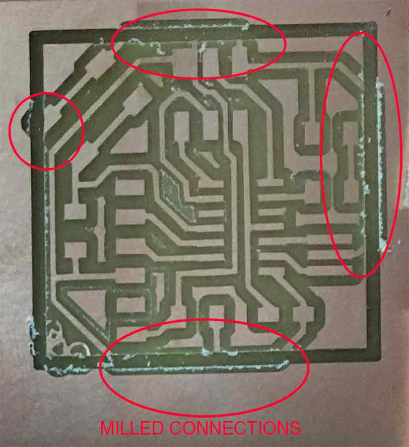
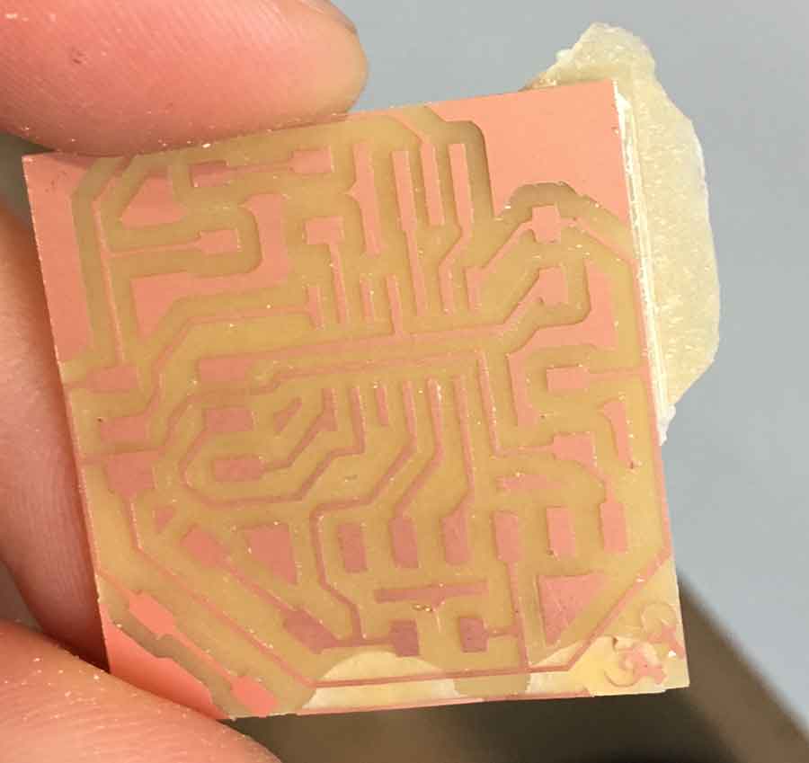
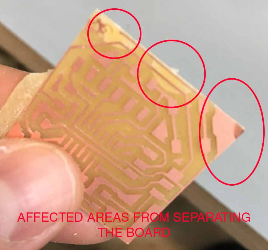
I reset the fabmodules and saved a new g-dcode for the outside. Send te traces againg to the machine with a anew board and afterwards the outline. This time the setting were right and none of my traces were compromised, but the miller didn’t go all the way trhough and when I tried to separate the board from the bed with a trowel I broke far of it. It didn’t affect any of the traces so Xavi told me it was alright to use it.
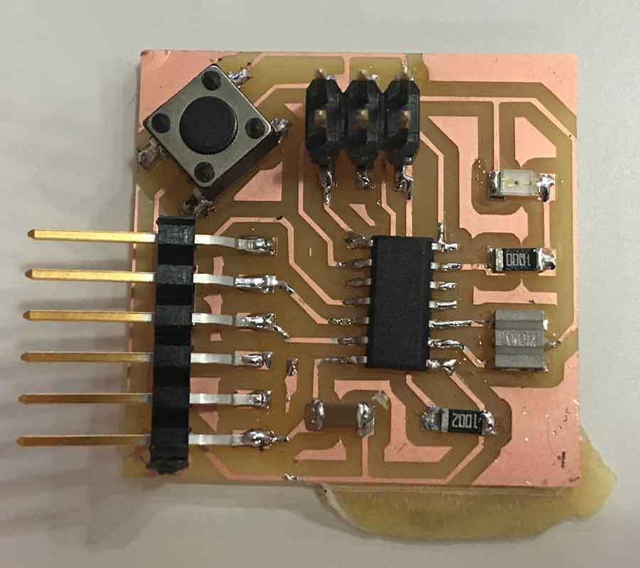
I went to the soldering table. Pick up all the components and did the “mise in place” and started soldering. I found that the most complicated to solder was the resistor and the button, they were the new elements too, so that might be the reason. Once that was done I checked with the multimeter that everything that was supposed to be connected was. Apparently seemed to be right.
BACK HOME <<<