Exercise 06 - Electronics Design
Assignment
For our assignment for this week, we have been set the following:
- Redraw the echo hello-world board, adding (at least) a push button and an LED (with current limiting resistor.
- Try out different EDA software to design our hello-world board
- Check the design rules
- Make the board
Background
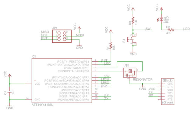
The echo hello-world board uses an ATTiny44 embedded controller. It has a 2x3 IDC header for programming and a 1x6 SIL header for communicating with another computer over a serial link. We use an FTDI USB-to-TTL serial device for communications.
The remaining pins on the ATTiny44 can be used to interface to other peripherals. For this assignment, we make use of 2 of the pins to interface to a pushbutton switch and an LED.
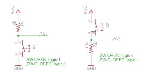
Interfacing to Pushbutton Switch
There are 2 basic ways to interface a pushbutton switch to a digital input on an embedded controller. We can either
- 1. use a pull-up resistor to tie the digital input to a logic 1 and connect the pushbutton between the digital input pin and ground. In this configuration, everytime the pushbutton switch is pressed, the digital input will be pulled low. When the pushbutton is released, the digital input reads a logic 1.
- 2. use a pull-down resistor to tie the digital input to ground and connect the pushbutton between the digital input pin and Vcc. When the switch is pressed, the digital input will read a logic 1 and when the pushbutton is released, the digital input will read a logic 0 because of the pull-down resistor.
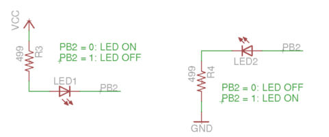
Interfacing to LEDs
Light emitting diodes (LEDs) are special types of diodes which emit monochromatic light when a current passes through it. Traditionally, LEDs have a forward voltage drop of 1.7V. Newer, high intensity LEDs may have forward voltage drops of 3.2~3.3V. LEDs are normally configured with a current limiting resistor to limit the amount of current passing through it to between 10~25 mA typically.
There are also 2 common ways of connecting LEDs to digital inputs:
- 1. use the digital output pin to source current to the LED
- 2. use the digital output pin as a current sink
Hello-world Board Using Eagle
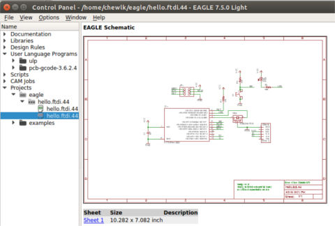
I started off by looking at Neil's hello.ftdi.44 board, tracing through the wiring and sketching the schematic for the board on paper. I then transferred the schematic to Eagle CAD.
One of the most challenging aspects of designing a circuit in EDA software when there components that you need is not available. In such cases, you would have to create your own custom parts for both the schematic and possibly the footprint. It is not difficult, just merely tedious, especially if you have to create a lot of components.
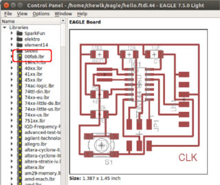
Fortunately for us, there is an Eagle library, (fab.lbr) available, containing most of the parts needed for many of the Fab Academy boards. To bring fab.lbr into Eagle, simply download the library and copy it to the Eagle library folder, /opt/eagle-7.5.0/lbr for Ubuntu 14.04 in my case, c:/eagle-7.5.0/lbr in Windows.
I started by creating a new project in Eagle's Control Panel, then a new schematic. I then added the parts that I needed for the hello.ftdi.44 board, mostly from fab.lbr. When wiring the components together, it is important to remember to use the NET command, rather than the WIRE command. If you want to link two different pins or traces together but do not want to run the wiring all over the place, simply assign the same NAME to the pins. The assigned names can be displayed using the LABEL command.
I changed the values and reference designators for the parts to match the values for the components used in my design.
Moving from Schematic to PCB in Eagle
To move from the schematic drawing to the pcb-layout package, simply select File/Switch to Board command. This brings up the pcb-layout, with a predefined board outline and all the components placed initially outside the board outline.
Move the components into the board outline, using the ratsnest as a guide to where to place the components. Components are rotated and moved around, so that the headers are at the sides of the board, ICs are oriented uniformly and there is minimal criss-crossing of the ratsnest. Some EDA packages even have a force vector and density histogram to aid the board designer.
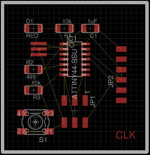
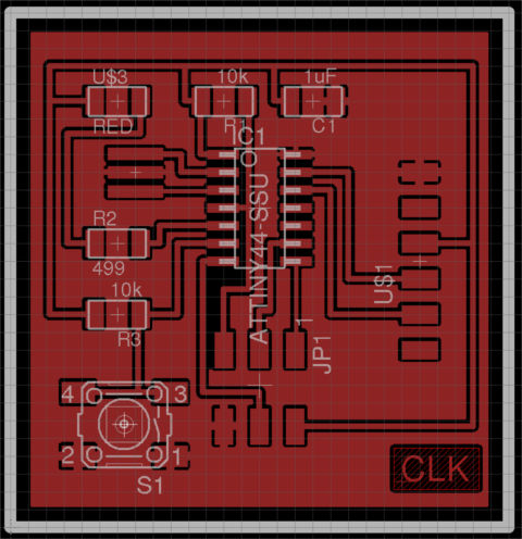
Once all the compoents have been placed, the next step was to route the board. Eagle has a reasonably good autorouter, but for a simple board like this, it is much easier to use manual routing. If you are not sure whether your board can be routed, you could use the autorouter to check how easy or difficult it is to route the board. To ripup an existing route, the RIP command is used. To ripup all the routes on the board, use the RIP; command.
For my pcb, I routed the tracks with a trace width of 16 mil (0.016"). I also added a copper pour aound the board, connected to the GND signal.
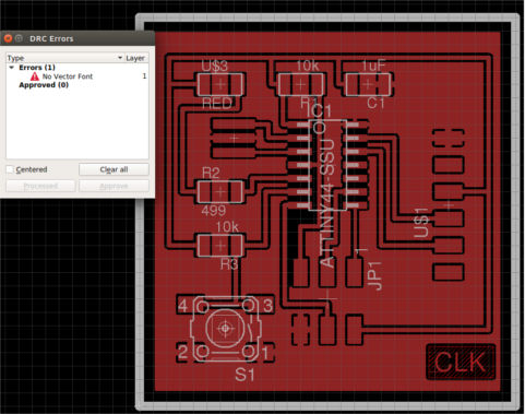
Design Rule Check (DRC)
To run a Design Rule Check (DRC) on my board, I first had to set up the rules for DRC. For my board, I set up the DRC with a wire-to-wire and wire-to-pad clearance of 10 mil and a minimum trace width of 12 mil, which is easily achievable using the pcb milling machines that we have.
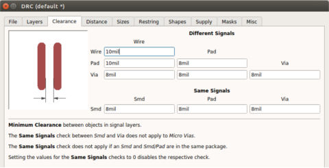
Happily, my board passed the DRC and I'm now ready to proceed to the next stage, which is to generate the gerber and/or g-code files so that I can manufacture (mill) my pcb.
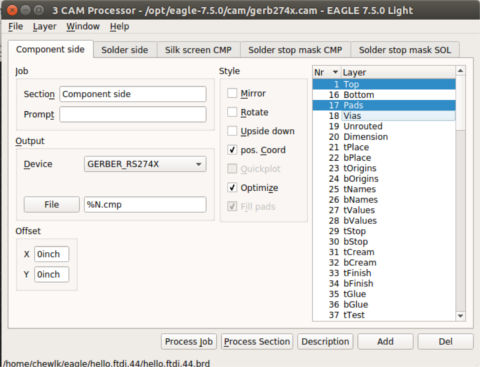
Generating Gerber Files
To generate Gerber files for the LKPF Protomat S103, click on the File/CAM processor menu option. Once the CAM processor dialog box opens, select File/Open/Job and select gerb274x.cam as the job type.
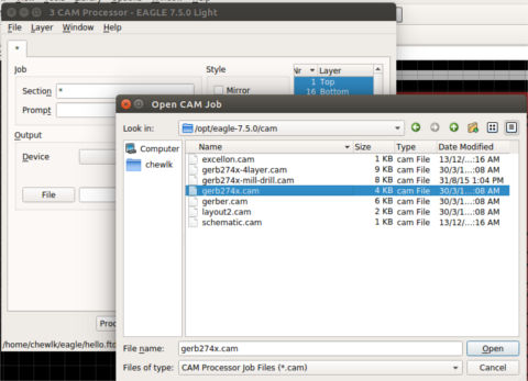
For single-sided pcbs, such as the ones we make during most of the Fab Academy assignments, we only need 2 files from the gerber output: component side (.cmp) and silk screen cmp (plc). For the silkscreen cmp gerber file, it is important to make sure that only the dimension layer is selected, as the board outline, which corresponds to the pcb cut file, is drawn on this layer. Click "Process Job" to generate the gerber files.
Generating G-Code Output
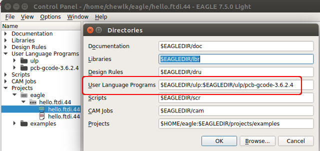
Eagle CAD can also generate g-code files for generic milling machines. To do this, you need to install the pcb-gcode ULP. Unzip the pcb-gcode files and save them in the Eagle ULP folder (/opt/eagle-7.5.0/ulp on my Ubuntu machine). In Eagle Control Panel, under Option/Directories, add the pcb-gcode directory to the ULP section and click OK.
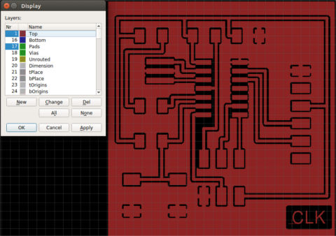
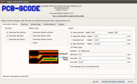
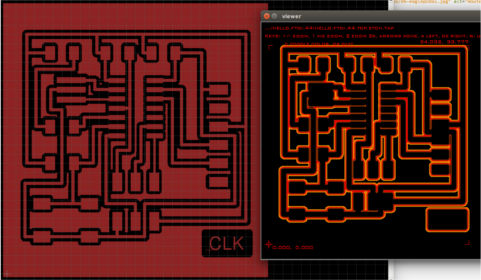
To generate the g-code for top copper layer, you first need to make sure that the silkscreen, component footprint, etc is turned off and only the Top and Pads layers are selected. Select File/Run ULP, navigate to the folder where pcb-gcode is installed and select the pcb-gcode-setup.ulp program.
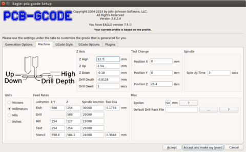
In the pop-up dialog boxes, configure the parameters for your specific milling machine. In my case, I used a mill depth of 0.18mm, single-pass isolation milling (min width 0.2mm) and a mill-bit of 0.2 mm diameter. Dirll depth was set as 0.8128 mm. Click "Accept and make my board" to generate the g-code for the top layer.
To generate the cut file for the board outline, repeat the procedure, but this time turning on the dimension layer and turning off all the other layers.
References for Eagle:
- 1. Install and Setup
- 2. Using Eagle Schematic
- 3. Using Eagle Board Layout
- 4. Creating g-code from eagle file
Design files for Eagle:
Hello-world Board Using Kicad
Kicad is a cross-platform, open source EDA suite and runs on Windows, OSX and many flavors of Linux. Kicad supports pcb layouts up to 32 copper layers and with a push and shove router. Kicad even includes a 3D viewer, where you can inspect your design in an interactive canvas. Sounds very interesting, well worth a look!
First step is to install Kicad. I did this on both an Ubuntu and a Windows machine. On Ubuntu, the steps are as follows:
    sudo add-apt-repository --yes ppa:js-reynaud/kicad-4
    sudo apt-get update
    sudo apt-get install kicad
The basic workflow in Kicad is as follows:
- 1. Create a project
- 2. Create a schematic using eeschema
- 3. Assign footprints to symbols and generate netlist
- 4. Create a board with pcbnew, importing the netlist from eeschema
- 5. Test the board using Design Rule Check (DRC)
- 6. Generate the gerber files for production
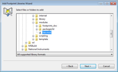
Once I installed Kicad, I looked for the fablab library, which Anders Haldin had created. Component libraries in Kicad comes in 2 files, a lib file for the schematic and a mod file for the footprint. These are copied into the library and modules folders of Kicad. In Ubuntu, the library folder is located at /usr/share/kicad/library and the modules folder is located at /usr/share/kicad/modules.
With Kicad running, I first created a hello.ftdi.44 project, which automatically created the schematic and pcb layout files as well. I then started up eeschema and proceeded to design the hello.ftdi.44 circuit.
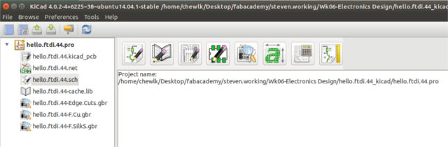
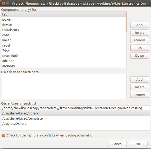
Once I was in the schematic design package, I added the fab library to eeschema. This is done by selecting Preferences/Component Libraries, then clicking the Add and Open buttons. Once the fab library has been added, I proceeded to move it up to the top of the list of libraries, so that the fab library would be the first library the system uses to search for components.
Since I was new to Kicad, I found designing the hello.ftdi.44 board in the software extremely frustrating. The first problem that I encountered was that the parts that I downloaded from Anders Haldin's link were supersized, compared to the rest of the components from the other libraries. After a series of email exchanges with the class, I realised that the old component library from Anders was not compatible with the current release of Kicad, so I had to put my design on hold, unless I wanted to create all the parts myself.
Another student, Liu Jun uploaded the fab library which he created by converting the fab library from Eagle to his website, so I proceeded to use that instead.
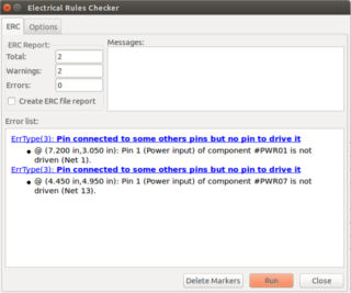
The next problem arose when I tried to run the Electrical Rules Checker (ERC) on my design. The ERC flagged out a lot of errors on my schematic. I realised then that I needed to put a "Place not connected" flag on all the unconnected pins in my design. The other ERC "error" which I couldn't resolve involved the power and ground signals. Kicad ERC reported a couple of type 3 errors and the location of these errors would change when I deleted and redrew the Vcc and GND connections, in an attempt to eliminate the error messages. Consulting Google, I realised that this was a common problem and that Kicad did not like it when component Vcc and GND pins are connected to power Vcc and GND through other parts, like resistors or capacitors. The basic advise was: "if you are sure your design is alright, just ignore the ERC error messages".
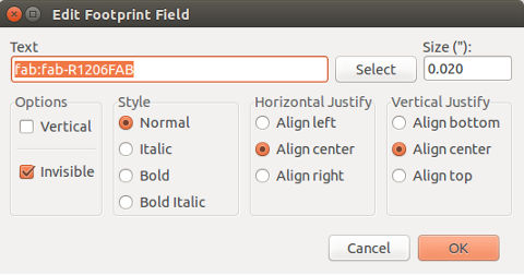
After all the issues were "resolved", I had my final schematic drawing. Before exporting the netlist for the pcb-layout package, I ran through each component in my schematic and checked to make sure that all of them were assigned the proper footprint. According to the Kicad documentation, the old method of assigning footprints was to use the cvpcb module. The new method was to right-click on the component, select Edit Component/Footprint, which I did. I then proceeded to generate the netlist.
Once I was in the pcb-layout package, I used the Footprint Libraries Wizard (Preferences/Footprint Libraries Wizard) to add the Fab library footprint module to pcbnew and verified it with the Footprint Libraries Manager.
Boy! Was I mistaken! For some inexplicable reason, pcbnew refused to recognise the footprints for my components. I kept getting error messages, stating that all of my components did not have valid footprints assigned to them.
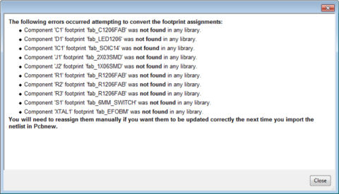
After consulting the cvpcb documentation and Google, I decided to revert to the old way of assigning footprints for my components, by using cvpcb.I had some difficulty assigning footprints to my components, until I finally realised that I needed to double-click on the footprint in order for it to be assigned. With that issue resolved, pcbnew was finally able to read the netlist and call up the required components for my pcb-layout stage.
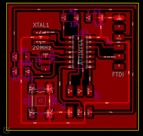
Board outlines are created by drawing a polygon on the Edge Cuts layer in Kicad. Once that was done, I proceeded to move the components onto my board outline. Just bring your cursor over the mass of components, type "g" and move the component onto the board. I also assigned the X=0, Y=0 origin at the bottom left corner of my board outline. From there, the next step was to route my board (using 16 mil trace width) and then do a copper pour over the empty areas of the board.
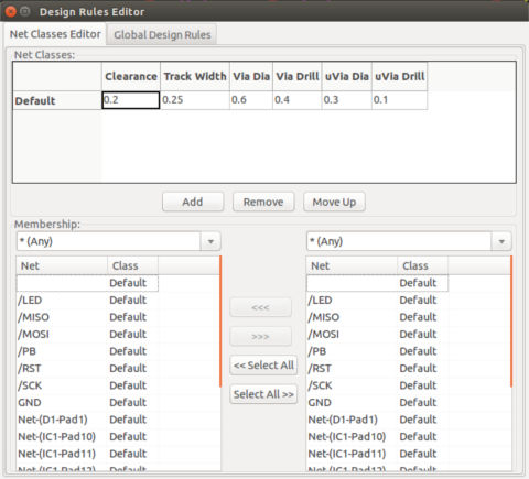
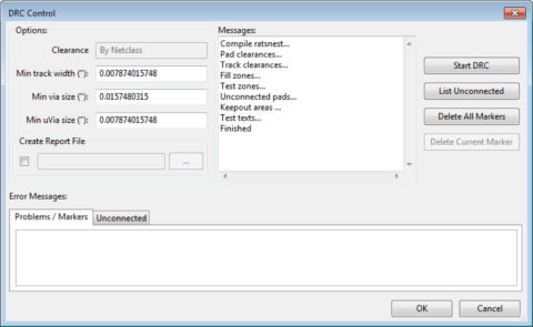
Design Rules in Kicad
Design Rules are set up via the Design Rules/Design Rules option from the pull-down menu. This brings up the Design Rules Editor, where Net Classes and Global Design Rules can be set up. The DRC tool is run after the Design Rules have been set up.
For my hello.ftdi.44 board, I used a trace width of 16 mil and clearance of 12 mil for the DRC. I also set up custom trace widths of 10 and 12 mil, in case I needed smaller trace widths, when routing between pins.
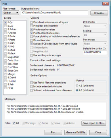
Generating Production Files in Kicad
To generate the gerber files for pcb production, the Files/Plot command is selected. This brings up Plot dialog box, where the user can select the plot format and layers to create. For my board, I generated gerber files corresponding to the top, top silkscreen and edge cut layers.
Kicad References:
Kicad files:
Hello-world Board in Kokopelli and Fab Modules
Kokopelli and Fab Modules were developed by Neil and extended by Matt Keeter as part of MIT's How to Make Almost Anything course. Fab Modules is available as a browser based application or as compiled source, executable on the local computer. The design UI for fab modules, kokopelli, is available as a separate application. Kokopelli and compiled fab modules run on both the Linux and OSX platforms. Installation instructions are on the respective websites.
I first tried out the compiled version of fab modules, as many of Neil's .cad example files are written in the previous version of kokopelli. The current version of kokopelli, version 0.2, is not compatible with the .cad file format. Matt has provided a retro mode, using the -r option, but it didn't work for me, so I stuck to the compiled fab modules and kokopelli v0.2.
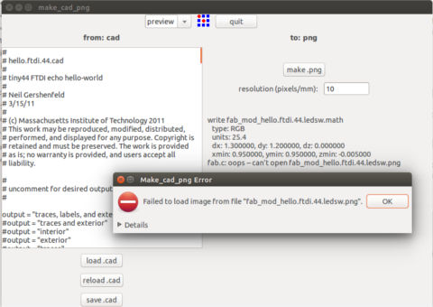
The other problem that I encountered is that the compiled fab modules did not work on my Ubuntu host machine. I got a Make_cad_png Error, stating that it failed to load image from the file "fab_mod_xxx cad file.png" that I loaded. However, compiled fab module worked fine on my MacBook and Xubuntu vmclient.
To create the modified hello-world board in kokopelli-retro, I started with Neil's hello-world cad file. As I needed a slightly larger board to accommodate the LED, pushbutton switch and resistors, I increased the board size slightly:
    width = 1.2
    height = 1.1
The next step was to add in the LED and the 499 ohm current limiting resistor. I then added the wiring to connect the LED and resistor to the circuit.
    # add resistor for LED
    R2 = R_1206('R2\n499');
    pcb = R2.add(pcb,XTAL1.pad[2].x-0.17,XTAL1.pad[2].y,z,angle=90)

    # add LED
    D1 = LED_1206('D1\nRED');
    pcb = D1.add(pcb,R2.x+.13,R1.y,z,angle=180)

    # wire LED to PB2
    pcb = wire(pcb,w,
        D1.pad[2],
        R2.pad[2])

    pcb = wire(pcb,w,
        D1.pad[1],
        point(D1.pad[1].x,D1.y+.06,z),
        R1.pad[2])

    pcb = wire(pcb,w,
        R2.pad[1],
        point(R2.x,IC1.pad[5].y,z),
        IC1.pad[5])
Adding the pushbutton and pull-up resistor was done in a similar manner:
    # add pull-up resistor for pushbutton
    R3 = R_1206('R3\n10k');
    pcb = R3.add(pcb,J1.pad[6].x-.15,J1.pad[6].y-.08,z,angle=90)

    # wire R3 to Vcc and PA7
    pcb = wire(pcb,w,
        R3.pad[1],
        J1.pad[2])

    pcb = wire(pcb,w,
        R3.pad[2],
        point(R3.x,IC1.pad[6].y,z),
        IC1.pad[6])

    # add pushbutton
    S1 = button_6mm('PB');
    pcb = S1.add(pcb,R2.x+0.1,J1.y+.1,z,angle=90)

    # wire pushbutton to PA7 and GND
    pcb = wire(pcb,w,
        S1.pad[3],
        point(R3.x,IC1.pad[6].y,z),
        IC1.pad[6])

    pcb = wire(pcb,w,
        S1.pad[4],
        point(S1.pad[4].x-0.11,S1.pad[4].y))
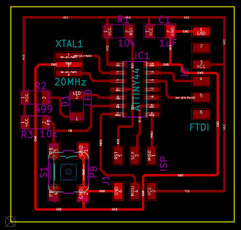
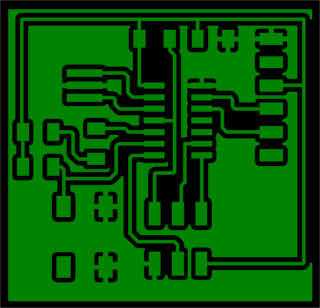
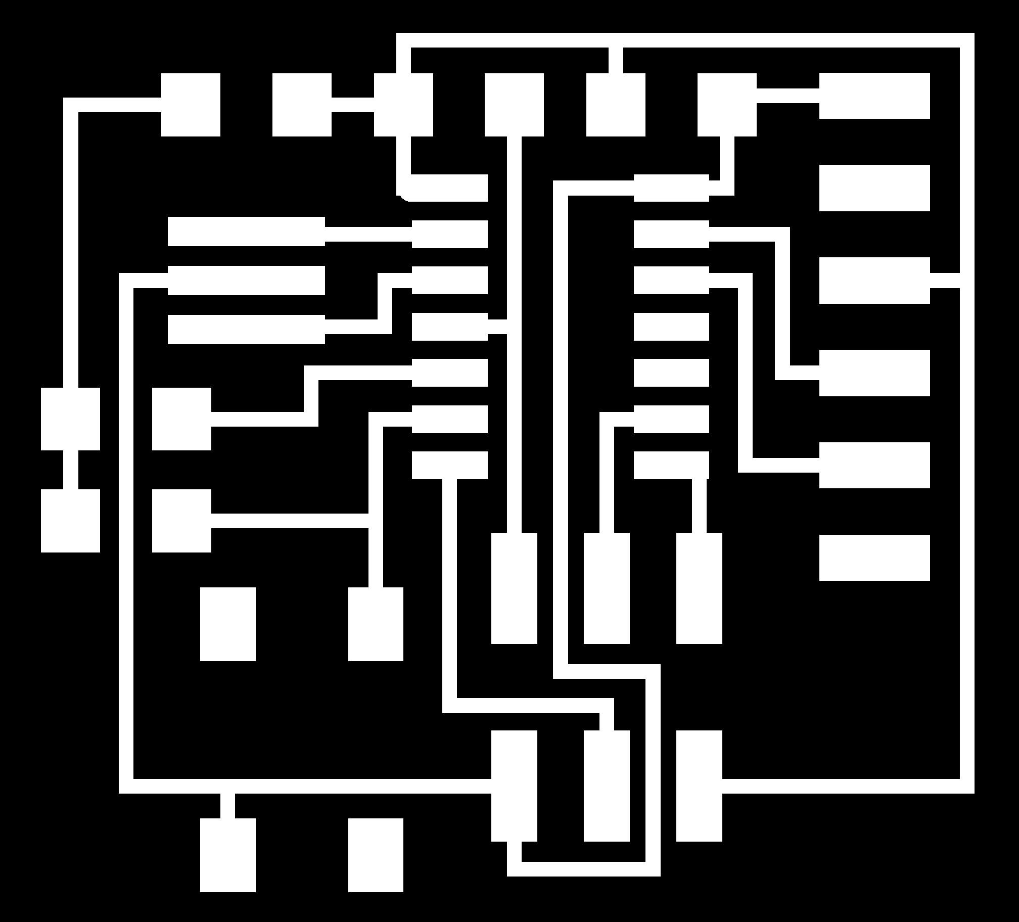
Each time I modified the code, I clicked on the "make png" button to check the results and edited the code until the components were placed at the correct locations and the wiring ran the way I wanted it to. My resultant modified hello-world board is shown below.
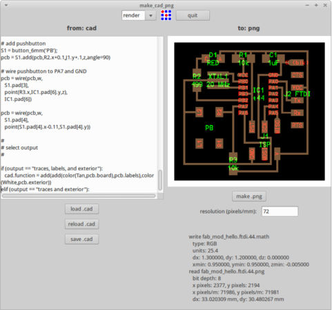
To generate the different png outputs (board, traces and outline), simply comment out the corresponding line in hello.ftdi.cad and click on the "make png" button. Each time the .png file is generated, it has to be saved to a separate folder and renamed, as it will be over-written by the next image file generated.
    #
    # uncomment for desired output:
    #
    output = "traces, labels, and exterior"
    #output = "traces and exterior"
    #output = "interior"
    #output = "exterior"
    #output = "traces"
    #output = "holes"
    #output = "solder mask"
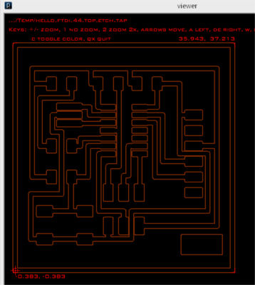
Fab Module version of modified Hello-world board:
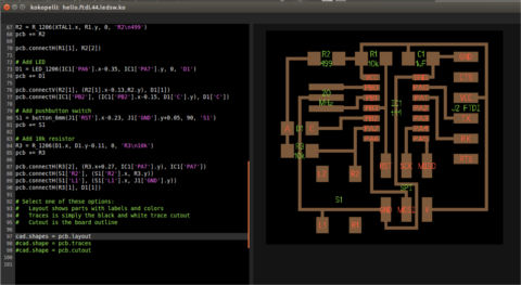
Creating the kokopelli version of the modified hello-world board is very similar. One problem is that the current version of kokopelli is not compatible with Neil's .cad file format. The other issue is that the pcb library that comes with kokopelli is very limited and for the modified hello-world board, I needed to create library parts for the resonator, LED and pushbutton switch.
Fortunately, creating pcb parts for kokopelli is not too difficult, as there are already sample parts in the .cad files. The format is very similar and it is not difficult to adapt it to the new format. The kokopelli pcb library file is a python file, located in the koko/lib folder.
I modified the pcb.py file to add the resonator component to the library:
    _pad_XTAL_EFOBM = s2d.rectangle(-.016,.016,-.085,.085)

    class XTAL_EFOBM(Component):
        pins = [Pin(-0.053,0, _pad_XTAL_EFOBM),
            Pin(0, 0, _pad_XTAL_EFOBM),
            Pin(0.053, 0, _pad_XTAL_EFOBM)]
        prefix = 'X'
And also the parts for the LED and pushbutton switch:
    _pad_button_6mm = s2d.rectangle(-.04,.04,-.03,.03)

    class button_6mm(Component):
      pins = [Pin(-.125,.08, _pad_button_6mm,'L1'),
        Pin(-.125,-.08, _pad_button_6mm,'R1'),
        Pin(.125,-.08, _pad_button_6mm,'R2'),
        Pin(.125,.08, _pad_button_6mm,'L2')]
    prefix = 'BT'

    class LED_1206(Component):
      pins = [Pin(-0.06, 0, _pad_1206, 'A'), Pin(0.06, 0, _pad_1206,'C')]
    prefix = 'D'
To create the modified hello-word board in kokopelli, I first imported the modified pcb library that I created earlier:
from koko.lib.pcb import *
Next step was to define the size of the board I needed and create the pcb:
    # Initialize the circuit board with xy position, width, and height
    w = 1.05
    ht = 0.95
    pcb = PCB(0, 0, w, ht)
After that, I added the components and wired the pins according to the schematic diagram. I have added some sample code to show how to add components and connect the pins in kokopelli format below:
    # We use an ATtiny44 as the brains of the programmer
    IC1 = ATtiny44_SOIC(0.58, 0.62, 0, 'IC1\nt44')
    pcb += IC1

    # Add an ISP header to program the programmer
    J1 = Header_ISP(IC1.x + 0.05, IC1[7].y - 0.24, 90, 'SPI')
    pcb += J1

    # Connect the in-circuit programming header to the chip
    pcb.connectH(IC1['PA4'], J1['SCK'])
    pcb.connectH(IC1['PA5'], J1['MISO'])
    pcb.connectH(IC1['PA6'], (IC1[7].x, J1.y-0.02), J1['MOSI'])
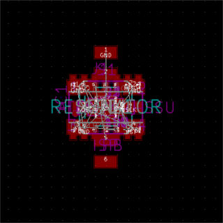
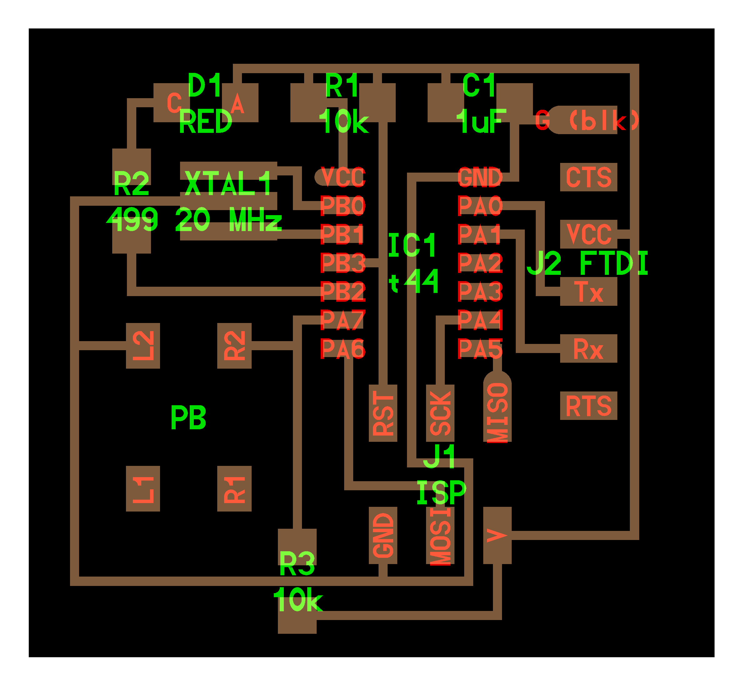
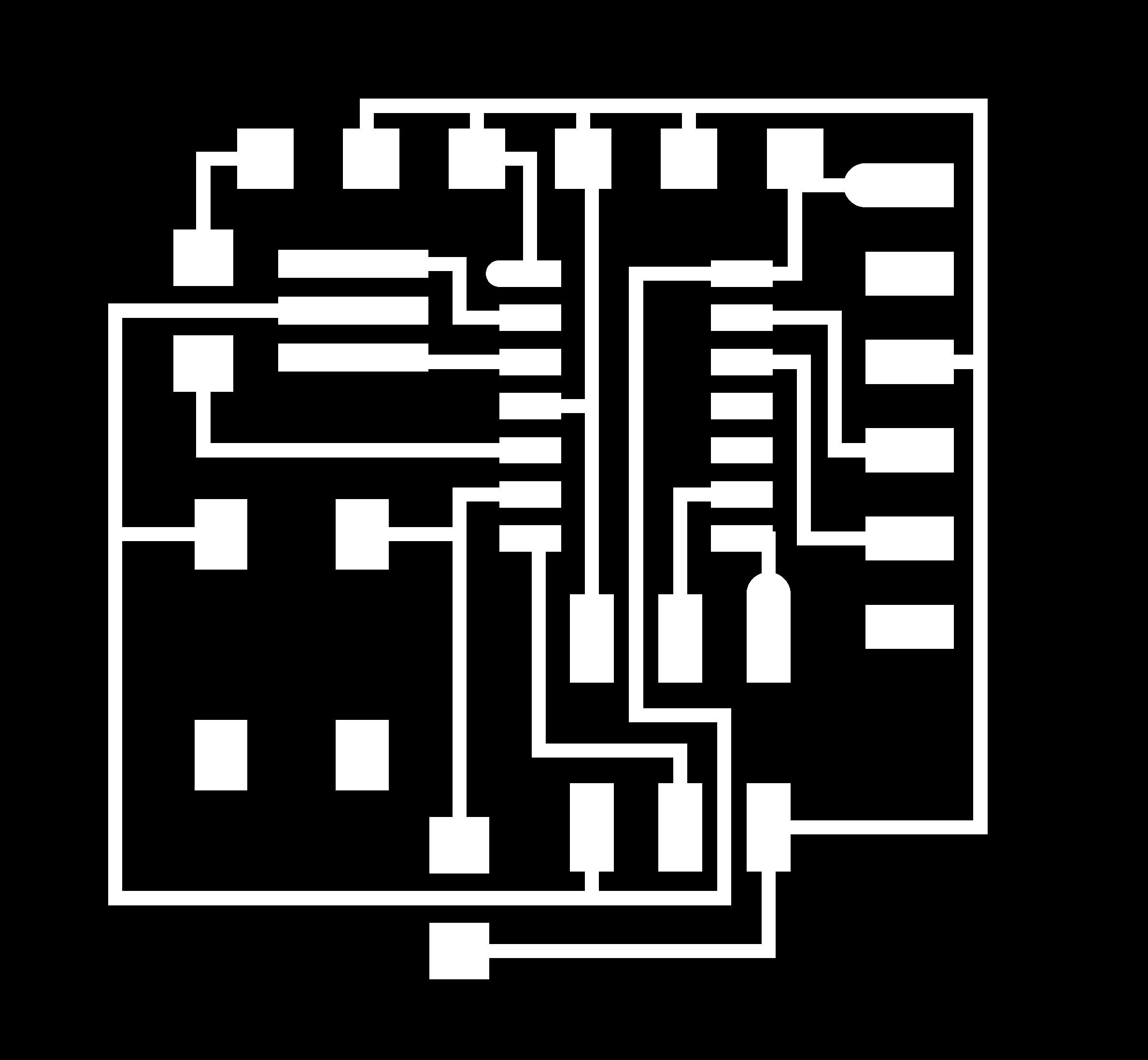
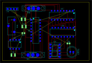
My completed modified Hello-world board, done in kokopelli, is shown below:
Just as in fabmodules .cad boards, simply uncomment the line corresponding to the type of output that is required:
    # Select one of these options:
    #   Layout shows parts with labels and colors
    #   Traces is simply the black and white trace cutout
    #   Cutout is the board outline

    cad.shapes = pcb.layout
    #cad.shape = pcb.traces
    #cad.shape = pcb.cutout
Kokopelli can export its output to different file formats including png, svg and stl. There is even a CAM panel, where kokopelli can generate output for the Roland Modela, lasercutters, shopbots and nc code.
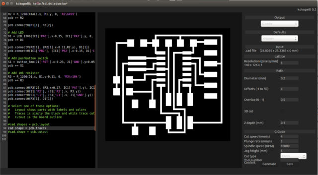
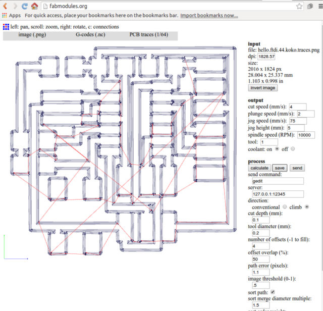
The .png file created by kokopelli can also be uploaded to online fabmodules, to generate the output files for the Roland Modela, shopbot or gcode for milling machines.
Kokopelli version of my modified Hello-world board:
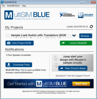
Multisim Blue
Multisim Blue is a special freeware release of the NI Circuit Design Suite, a popular circuit analysis, simulation, schematic capture and pcb layout software from National Instruments. NI's Multisim package also supports SPICE co-simulation, where microprocessors and embedded controllers can be simulated. The co-simulation package in NI Multisim is limited to the PIC1684FA and Intel 8051/52 microcontrollers only.
Once Multisim Blue has been installed and started up, the splash screen appears. Click the "Launch Multisim" button to start Multisim, the schematic layout package.
>
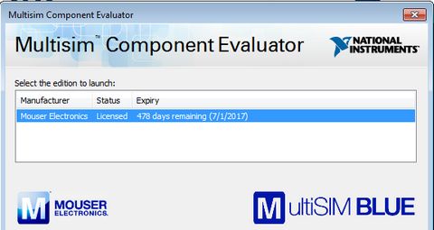
Multisim Blue is released by Mouser, under NI's Multisim Component Evaluator and Ultiboard Component Evaluator agreement. According to a review article in PCBShopper, Mouser's agreement with NI for Ultiboard expires one year after release and that for Multisim Blue expires in July 2017.
The same article also states the following limitations of Multisim Blue:
- maximum of 65 components per schematic, excluding grounds and power sources
- single-sheet designs only
- only two custom components can be created per design and they cannot be saved to a parts database for reuse in other designs
- there is no forward annotation from schematic to pcb; if you change your schematic after the pcb has been laid out, you need to re-layout your pcb from scratch
- back annotation from pcb to schematic is also not supported
To add a component to the schematic layout, use the Place/Component command. The component value and footprint is selected at this time. I found the component library of Multisim Blue to be extremely limited, only a fraction of what the full Multisim package has. Mouser has indicated that all 100,000 components in its inventory will be in the Multisim Blue component database. It's been almost 1 1/2 years since the release of Multisim Blue and its component library is still extremely limited. Coupled with the fact that each design can only have up to 2 custom parts, which cannot be saved to the parts database, this makes Multisim Blue very unattractive as a design tool for Fab Academy.
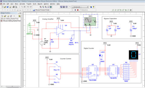
Since I couldn't layout the hello-world board, I decided to use one of the example circuits that came with the software, the Mouser Getting Started Final circuit instead. Multisim Blue supports analog, digital and mixed signal simulation. There are also a number of virtual instruments, which can be used to monitor &/display the simulation results.
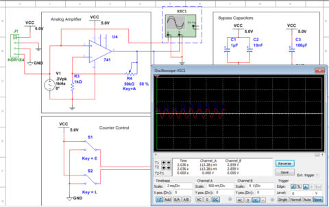
To move to the pcb layout package, click on Transfer/Transfer to Ultiboard/Transfer to Ultiboard Component Evaluator on the top menu bar. This calls up the Ultiboard pcb layout package. Components are placed outside a default board outline at the start.
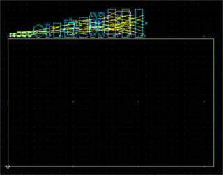
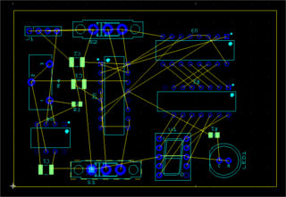
The board outline is first resized to the desired board size. You can use the autoplace feature to do an initial placement of all the components, then move the components around to get the optimal placement. The ratsnest is use as a guide to the optimal placement. Ultiboard uses push-and-shove component placement, which is a very convenient feature.
The autorouter in Ultiboard is a gridless autorouter with push-and-shove capability. There is also a follow-me function for the autorouter. To configure the autorouter/autoplacement, clkck on Autoroute>Autoroute/place options at the menu bar. This brings up the Route Options dialog box.
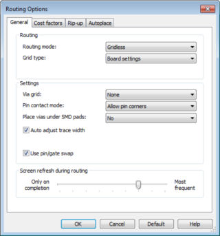
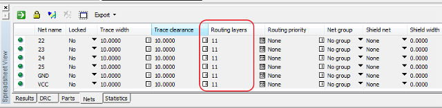
You can specify whether you would like to route on the top, bottom or both layers by selecting the Nets tab in spreadsheet view, selecting the nets and clicking on the Routing layers column.
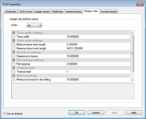
The Design rules can be set by clicking on Options/PCB properties on the top menu bar. This brings up the PCB Properties dialog box. Click on the Design rules tab to configure the DRC for your board.
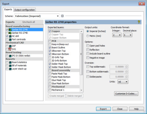
When your board is finally ready, you can export the design to gerber files for pcb manufacturing. The Gerber settings dialog box is reached by selecting File/Export from the top menu bar. This brings up the Gerber dialog box, where you can specify the gerber format, BOM and whether you want to also export a dxf or svg file for mechanical CAD assembly.
I did not design my Hello-world board using Multisim Blue as the lack of library parts and limitations of this software, where custom parts are limited to 2 components per design and more importantly, cannot be saved to the parts database for reuse meant that it was a pointless exercise.
Milling the PCB
At Fablab SP, we have 3 types of pcb mills:
- An LKPF Protomat S103
- A Roland iModela
- PCB2020B China mill
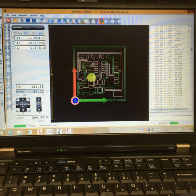
My first task was to convert my board layout to gcode for the PCB2020B. I've designed the Hello-world board on a variety of EDA software, but Eagle CAD is still my primary design software at this point in time, so I used the pcb-gcode ULP to generate the etch file for our mill.
My settings for PCB-gcode were:
- Tool Diameter: 0.12mm
- Milling Depth: 0.18mm
- Single pass isolation milling @0.12mm
The .etch file generated by PCB-gcode was then imported into the CNC-USB, PCB2020B's milling control software. I then set the home position for the milling machine. This is done by moving the X & Y axes to the bottom left corner of the target pcb. I then zeroed the Z-axis, adjusting the Z-axis until the tip of my milling bit just touched the surface of the pcb. Once the machine was zeroed, pressing the "PLAY" button started the milling process.
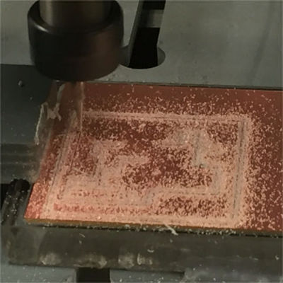
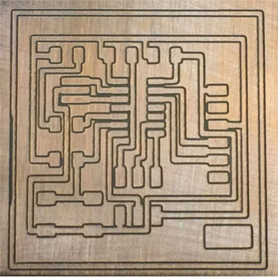
I cannot over-emphasize the importance of checking the milled pcb with a multimeter for both continuity and short circuits at this point. I've done a visual inspection of the pcb on a light-box and against the light, but given how close the traces are on an SMB board, spending a bit of time here can save a lot of headaches later.
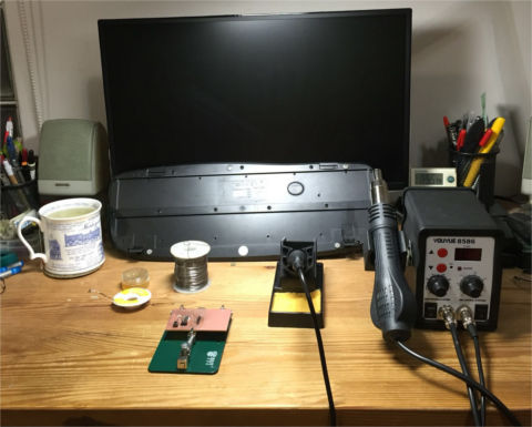
Stuffing and Soldering
The last step for this assignment is to populate my pcb and to solder all the components in place. We are quite fortunate that we do have some access to facilities at our fablab after office hours, but most of us, myself included, do have a life outside of work and the Fab Academy course, which means being able to do some of the assignment at home as well :)
After the soldering has been completed, it is again important to trace through the circuit with a multimeter to check all the connections for continuity and short circuits, as it is easy to make mistakes when soldering SMD circuits. A short circuit can easily mean either your board or computer going up in smoke...
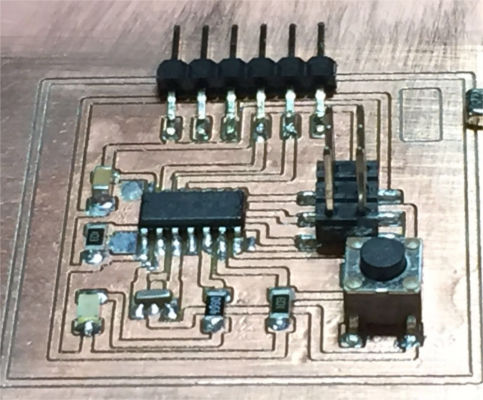
One issue that I would like to highlight - I used the Eagle fab.lbr library for schematic and pcb to design and layout my circuit. I found that the footprint for the pushbutton is a little too small for the actual component that we have in our inventory, so I had to bend the legs of pushbutton a bit closer, to make it fit the pads.
Testing the Board
I'm very interested to check if my board works, so as a final step, I've decided to test it with the Hello Echo demo program, followed by exercising the pushbutton switch and LED, perhaps getting the LED to blink a few times after each time the pushbutton is pressed.
I haven't completed this part yet, but stay tuned...
Done - you can check the results in Week 7's assignment