Electronics Production

During this week I have tried to make an in-circuit programmer

software used during the project

Inkscape
Inkscape is a good tool to vectorize the raster images. So it was used to transform the png to files with pcb board schema to vector files that can be used by proprietary software of the CNC machine
Eagle
Eagle is the software that permit to be in PCB production. So I used it to see the principal schema, list of required components and locations for components
Vcarve
Proprietary software that permit generate files acceptable by the CNC machine from the vector files (in fact from the dsx)

hardware used during the project

Roland-srm20
Micrometric desktop milling machine. We use it to mill PCB.
End-mills
1/64" and 1/32" endmills. 1/64" is used to etch traces on PCB, 1/32" is used to cut PCB and make holes.
PCB plates
FR-1 PCB plates. We can use FR-1 or FR-2 PCB plates because they are produces as composite material by using the phenolic resine and compressed paper instead of epoxy resine in FR-4 - that is much more harder and end-mills are used much faster on FR-4. As well the dust produced by epoxy is not good for the health so the respirator mask is requried.

Assignments

Make an in-circuit programmer USB key

In our fablab we do not have yet operational the CNC micrometric milling machine. So we used the big CNC machine to cutting the circuit board... Let see the results...
Update! Now we have a Roland-srm20 machine so we started milling all our PCB. Click hereto see production process using the roland machine.

Before we start - Safety is the number one priority.

CNC board building

First try

We use bit that quiet big...

And the machine is a monster in if we compare to the task it should do. But we use what we have to try to arrive to result. Hope for the next time we will have machine micrometrical for PCB producing as defined in pre-requirement of handbook.

Let see what we have...

After passing some try and some alignment and re-try and re-alignment... And re-re-try we have some interesting results.

Some of them drilled too deep...

Some of them are not enough deep...

And other are not deep again

Some of them small.. some of the big...

Milling is not really clear.

At the end of the day we have something that looks like enough good... (Visual control + multimeter to check if no short circuit where it should not to be and if connection exist where it should exist.) We do some manual cutter finishing and we want to pass to next step. Soldering...

Let pass to soldering.

Some main rules for soldering that we need to follow.

Comp. Orientation
Components may have (or have not like resistors) importance of direction (diodes, chips, transistors, some kind of capacitors, etc...).
Soldering direction
We do soldering from center to outside. And from top to bottom. This rule is important to always have correct access to component we will solder.
Antistatic
When we start to work with electronics, (as now is winter with some days cold and dry it becomes even more important) we can have static electricity that may destroy the electronic components on the board. So always touch the "ground" (or use special bracelets) when you work with electronics.

We use two different methods of soldering. For the ATTiny we use the solder paste and air heating machine... Sic... we have only the big air heating machine....

Another huge one...

But we can use it if we will use the solder paste only for the chip. And the rest we will do using the soldering iron.

So we put the chip on place, we fix it by using the thermo-ribbon, we put the solder paste over the legs of the chip and we start to heat it. In few seconds, when the temperature pass over the limit of the paste it start to melt and solder the component. We cool it down, do visual control and turn the thermo ribbon to other side of chip and we repeat our operation on second side of the chip.

Solder paste

Special thermo tape

And here is result

As we have huge air heating, we can not use the same solder paste method for other components as we can not heat only the one components in the time... The air flow is too wide. So I will use the soldering iron to fix another components.

Heh... little error. We have the crystal for the hole-based soldering and I forgot about it so no holes drilled in my board on this step.
So I started my soldering using the iron for the components located close to center and up of my board. As well we attached the schema on the board so we do not miss which component goes where.

Soldering using iron

Attached to board schema. It permit to check components and its orientation during production process.

And here is result

Yoohoo... Tuesday evening we build another card V2 using the smaller and more adapted bit on the same monster machine..

V2 with better quality

V2 with better quality

But need prepare

We cut bridges missed by machine

We solder chip first side

And the second side

Yoohoo 2... Tuesday evening we build another card V3 :) Now we used better source plate. So quality becomes really good! Probably this card becomes the final that may be used for producing the key.

Time is too close to 20h - so no time to solder components. Will do it next week to make my card working. Below you can see video of soldering by using the soldering paste.

Here is how this big machine works...

Electronic production with Roland machine

In electronic production using the Roland-srm20 machine we use the following process workflow. As the source we need to have a .png file of our traces, of cutout (dimension of PCB), and holes if any. These files may be produced by different way and we will see this in next weeks (how to produce these files using the Eagle CAD software for example). In this production week I will use already existed image of the PCB.

Step1: Prepare gcode files

Using the Fabmodules we transform the black and white image png file to Roland gcode file. For this we use following actions (cf. images below). What is important to remeber: white on image will stay untouched by the endmill, black will be cutted by the endmill. So when you do outcut or traces or holes - check that black and white on image has correct meaning. If it is not the case - use invert button on the fabmodule.

Step2: Visual control

Check if the traces proposed by the fabmodules are cover all required paths. In fact the thickness of the tool 1/64" is about 0.4 mm diameter - so the distance between two separated path should be at least 0.4mm and sometimes on curves it not the case. So the tool can not pass and the isolation of path will not be done. It can happens when you are not the source of the file and you can not be sure of result. Example of this case is present below.

To resolve such kind of cases you need to re-work your PCB in Eagle (re-check the rules and control application of rules. cf next weeeks). Or if you have thin tools to make isolation - you can use it to cut such kind of PCB.

Step3: Milling

Prepared .rml files need to be transferred to machine.

On the Roland we need to use manual leveling of Z-0. So you need to process it in the way it is defined in your LAB. We use the "thin paper method".

Step1: Etching traces

Preparation: We set the X an Y to 0 point over the left bottom border of our PCB plate. Change the milling bit to 1/64" to make traces. Then execute level Z-0 procedure. And load to machine the first trace file and then click to "Output" button. ATTENTION: always be present near machine and be ready to click on PAUSE button if something goes wrong.

Step2: Cut holes

We need that PCB stay attached to its place when we cut holes - so this step is goes before the cut the outpath.

Preparation: We change the milling bit to 1/32" to make holes and we proceed the Z-0 procedure. ATTENTION: XY must stay untouched.

As the holes and outcut done by same tool - we join two cut in same step.

Step3: Outcut

We load in same time second file with out cut and we check that the order of files is: holes -> out cut. And we start cutting by click "Output" button. ATTENTION: always be present near machine and be ready to click on PAUSE button if something goes wrong.

Step4: Visual control

On this step we check if after cut our board has all traces present and they are isolated.

For this we use magnification lenses, and bright light - we can see in transparence for the good isolation (if our PCB is one side).

Step5: Soldering

For soldering we use tin for connect componets to PCB, and we use FLUX to simplify soldering process.

Soldering need to be done as remarked above - from center to outside, from top to bottom. It permit simply connect components.

Step5: Visual control and cleaning

As well - visual control again. We check that after soldering no rest of tin on PCB that may crate a short circuit on the board. We check that all pins of our components are connected. And we fix errors if we found that some traces are missed (if we found it on steps before for example)

PCB need to be cleaned by acetone + alcohol if we have used Flux during the soldering. It is active chemistry that may add corrosion to your PCB. (it may become dark or rockford colors pcb :) )

Step6: No smoke test

We connect our device via the ISP programmer to computer and we check that ISP programmer do not show error of PCB and as well no smoke from device ;-) - so it probably works.

Step6: programming

Using the ISP we programm our PCB. I will explain this process in more detailed way in next weeks (Embedded programming and so on). So see it in next week.

If this step passed well - we are good! And our PCB is produced.

Summary

Just for fun - I think it is cool to know how long it take from scratch to produce one working PCB cart using this method. So my estimations are below

Eagle file
If we have not big board (around 10 components on PCB), and if all components are present in the library - it take about 1..2 hours to generate files ready for fabmodule
Fabmodule
About 15 minutes to execute everything related to fabmodule (Usually we do pass by GIMP before because outcut generated by Eagle is not always good - I will explain it in next weeks)
Roland
Roland machine full pass including 2 changes of tool and 2 times leveling Z, attaching the PCB board and milling will take about 30..40 minutes. With preparation of fabmodule you can count 1 hour for everything.
Soldering
It will take about 1 hour. Depending on components, preparation, visual controls and cleaning.
Programming
It may take hours... Pushing of code to the controller is fast - it take seconds, but writing the code - may take days... But let take 4 hours as an average.
TOTAL
So - total is about 1 full working day from an idea to real working PCB (it may variate from 4 hours in best score up to few days (months) of debugging / programming / re-creation of PCB and so on..)

FabISP

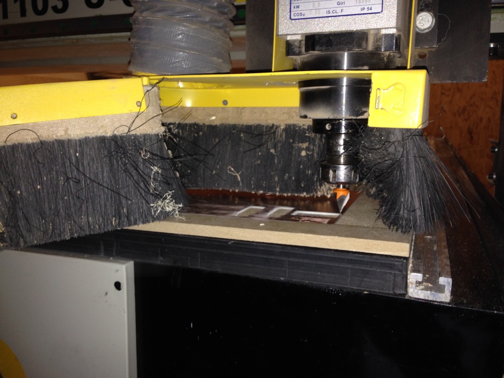
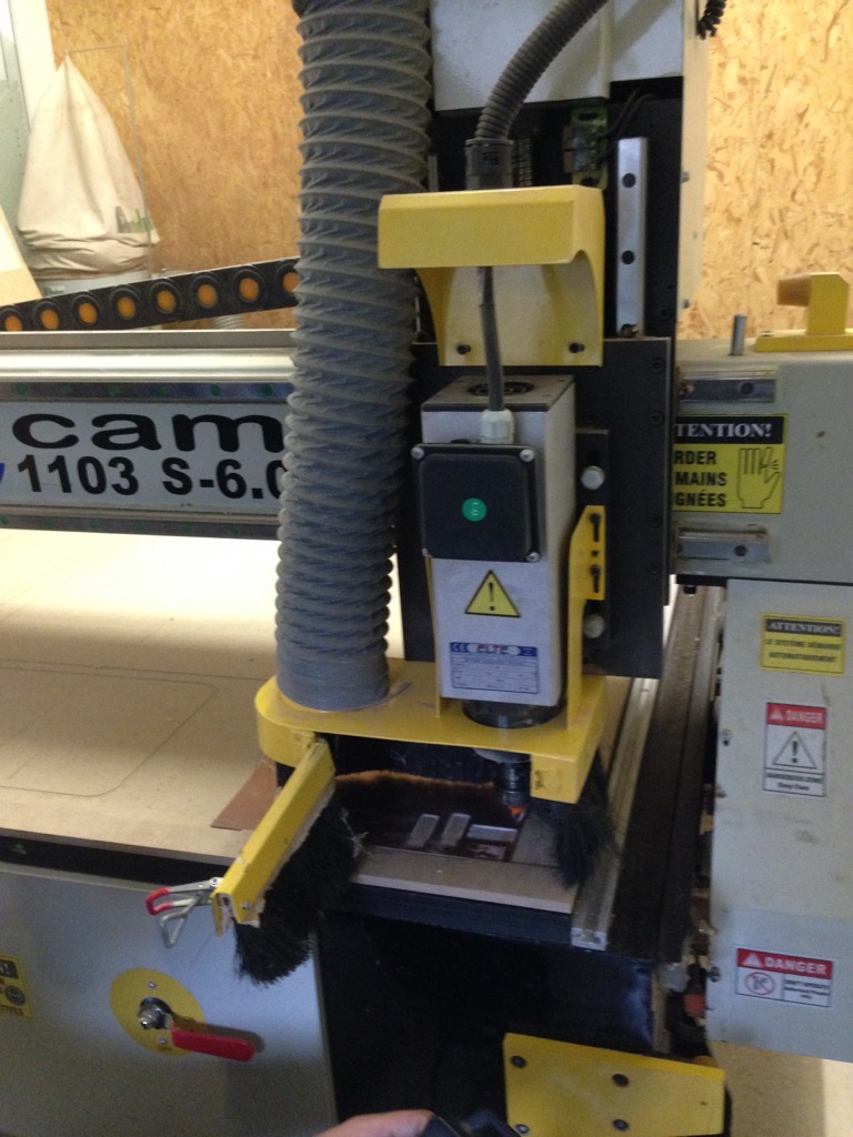
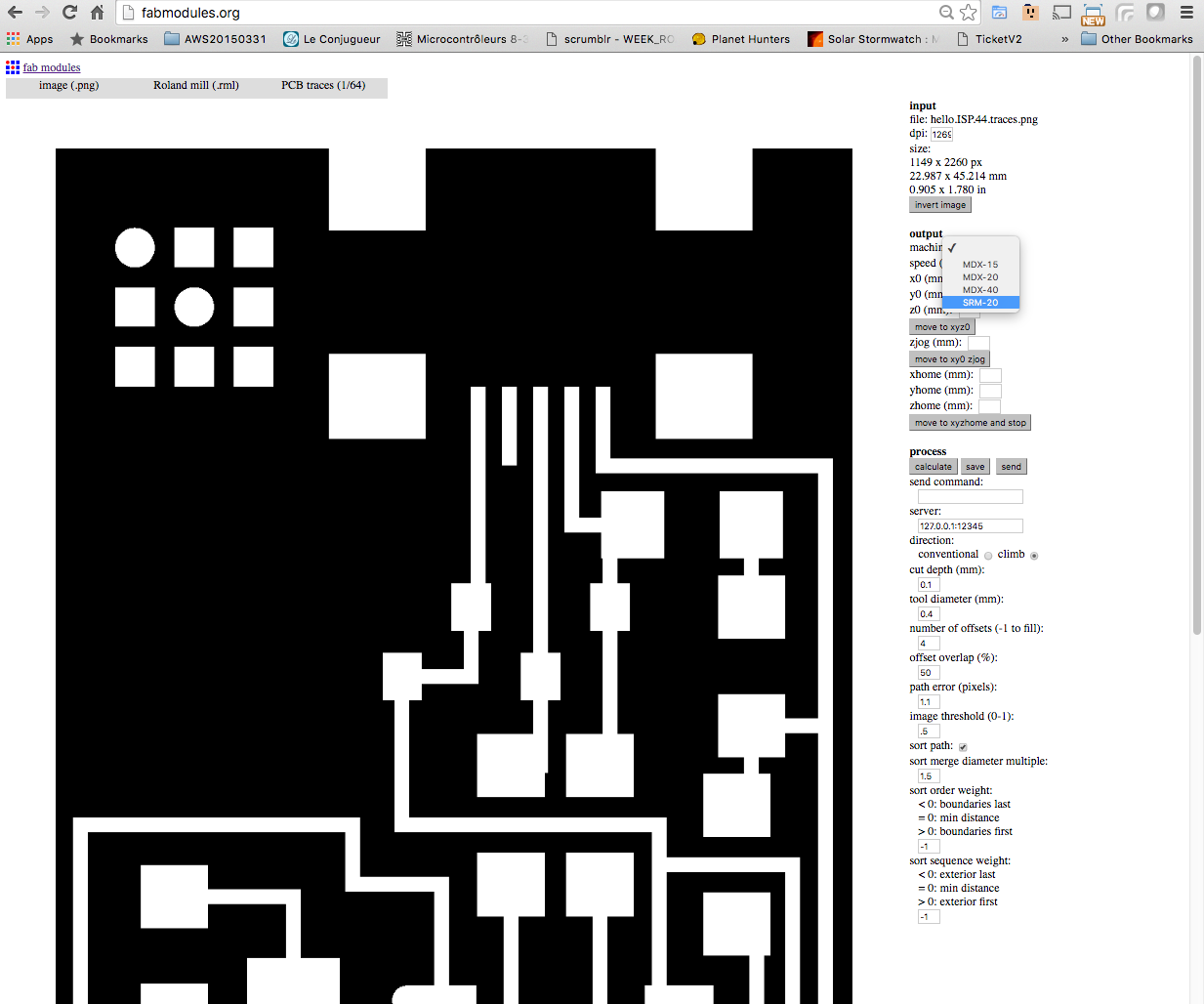
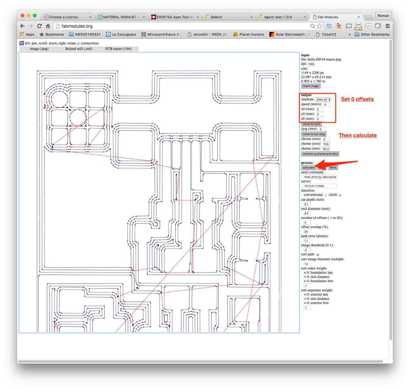
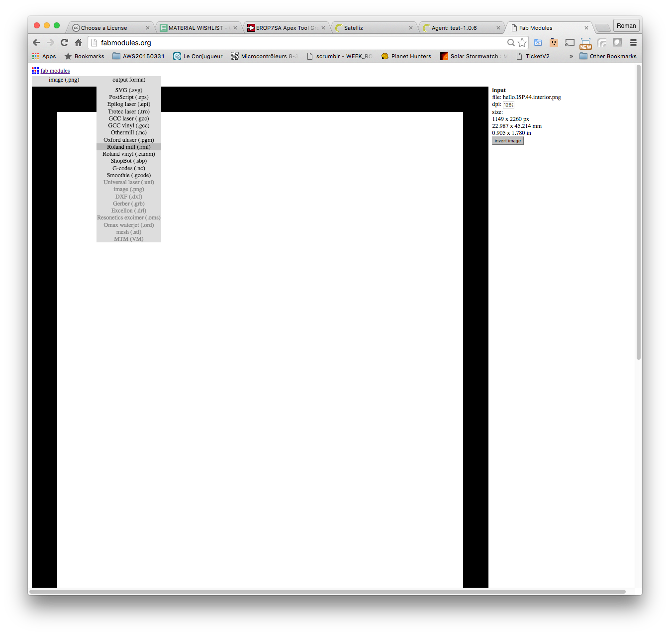
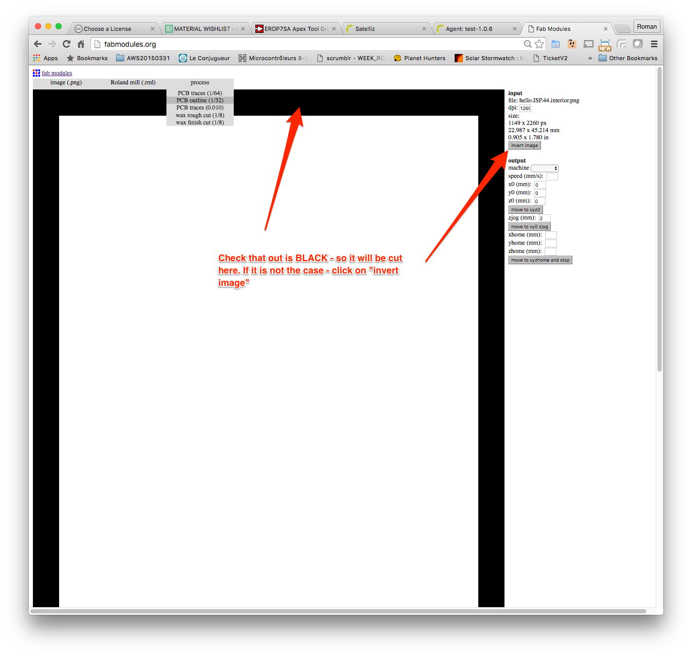
Now we have Roland machine and let finish the FabISP production.

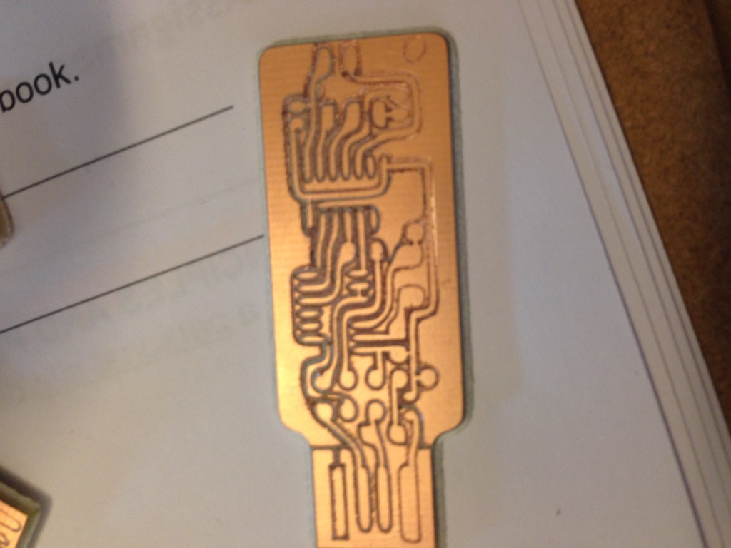
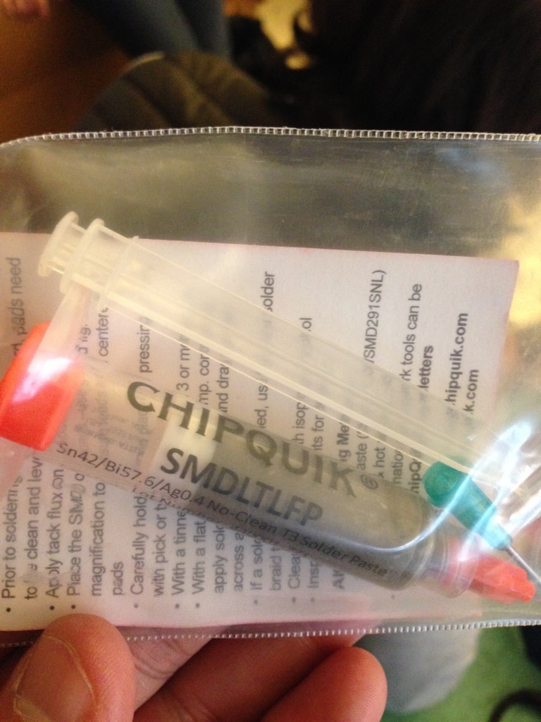
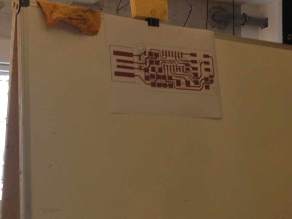
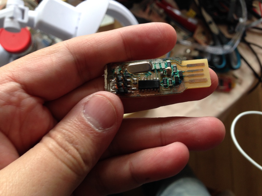
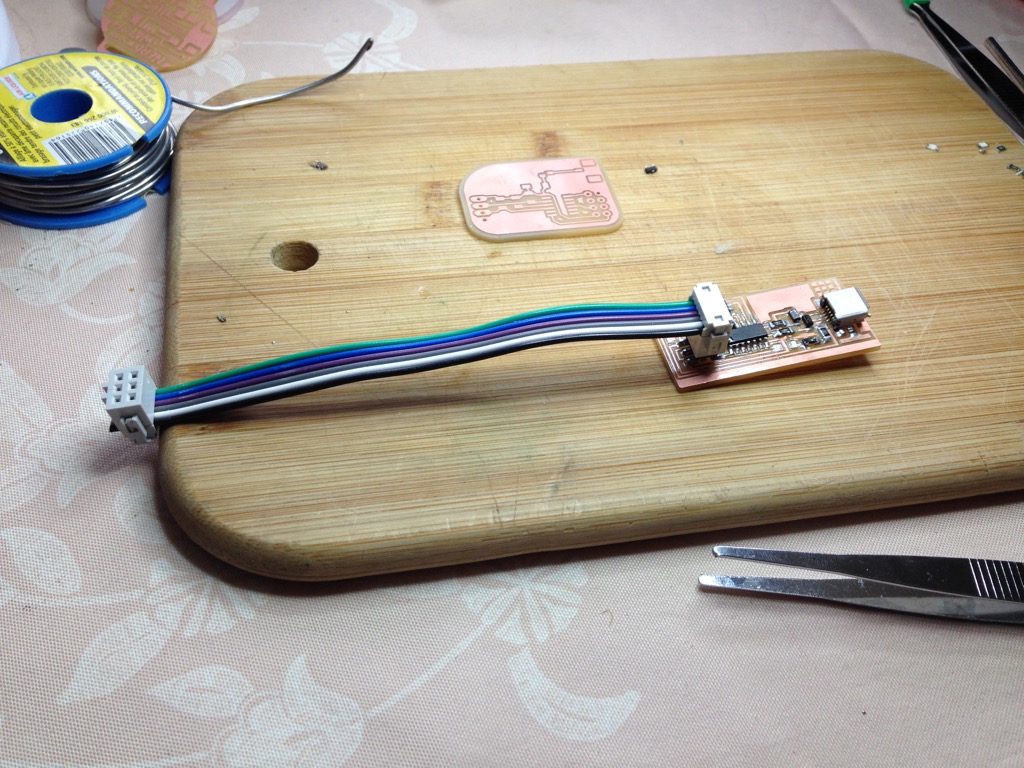
After some ivestigation in stock - looks like it is ok to make a FabISP that is in the list of schedule page. We pass a lot of time of production the FabISP directly connected to USB, without cable, but finally IMHO it is better to use proper cabled version 
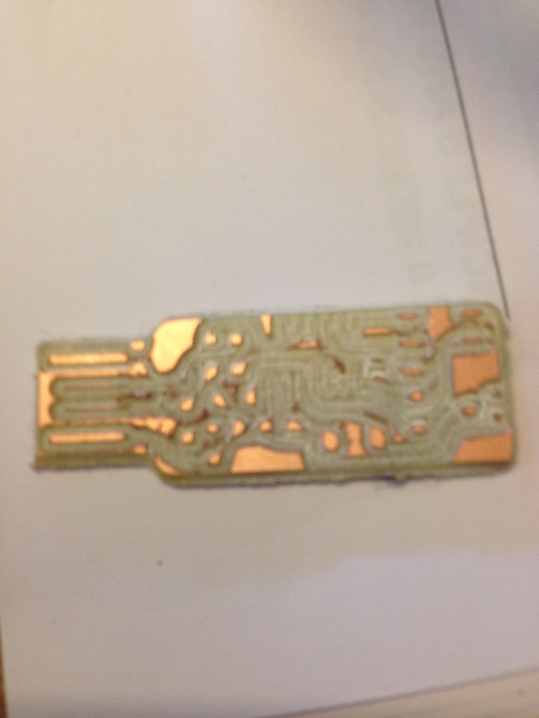
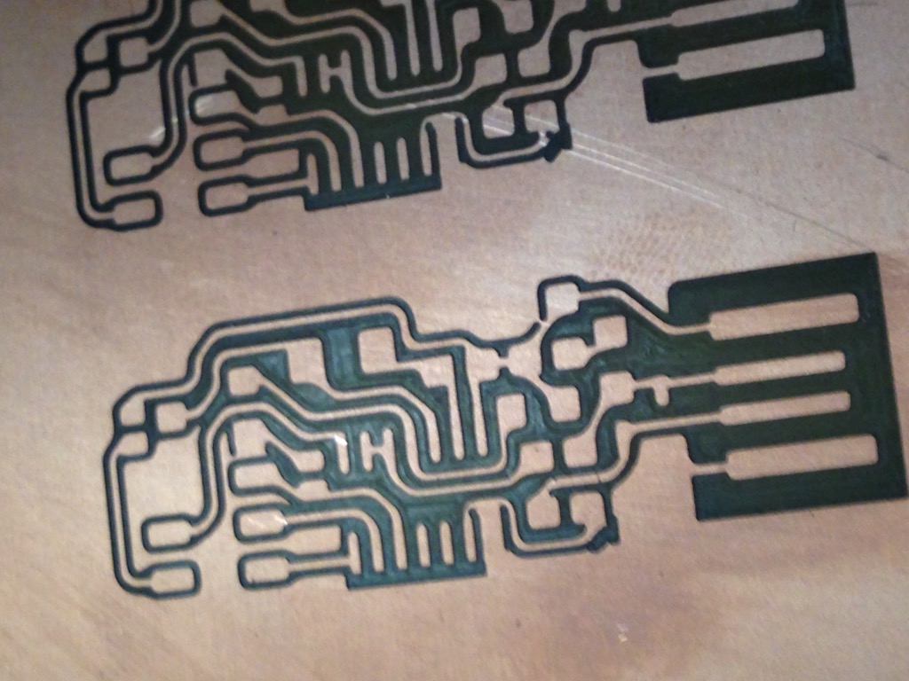
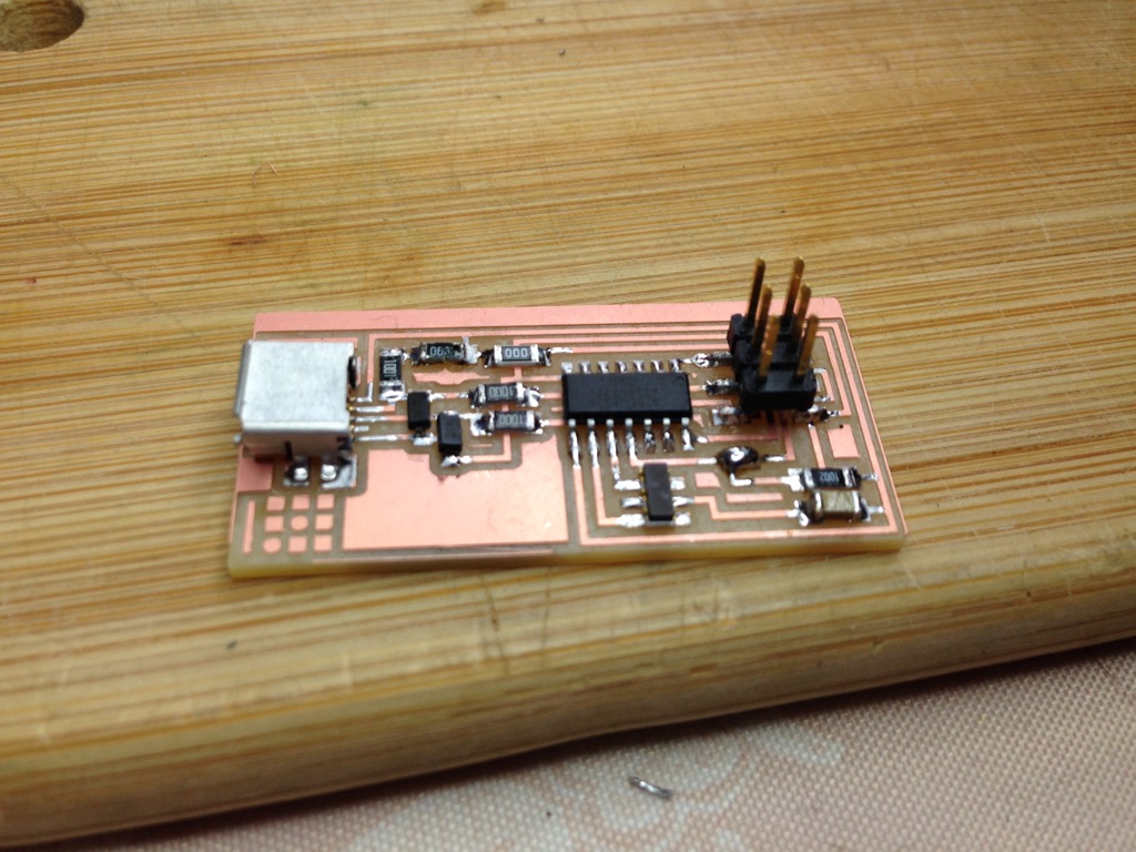
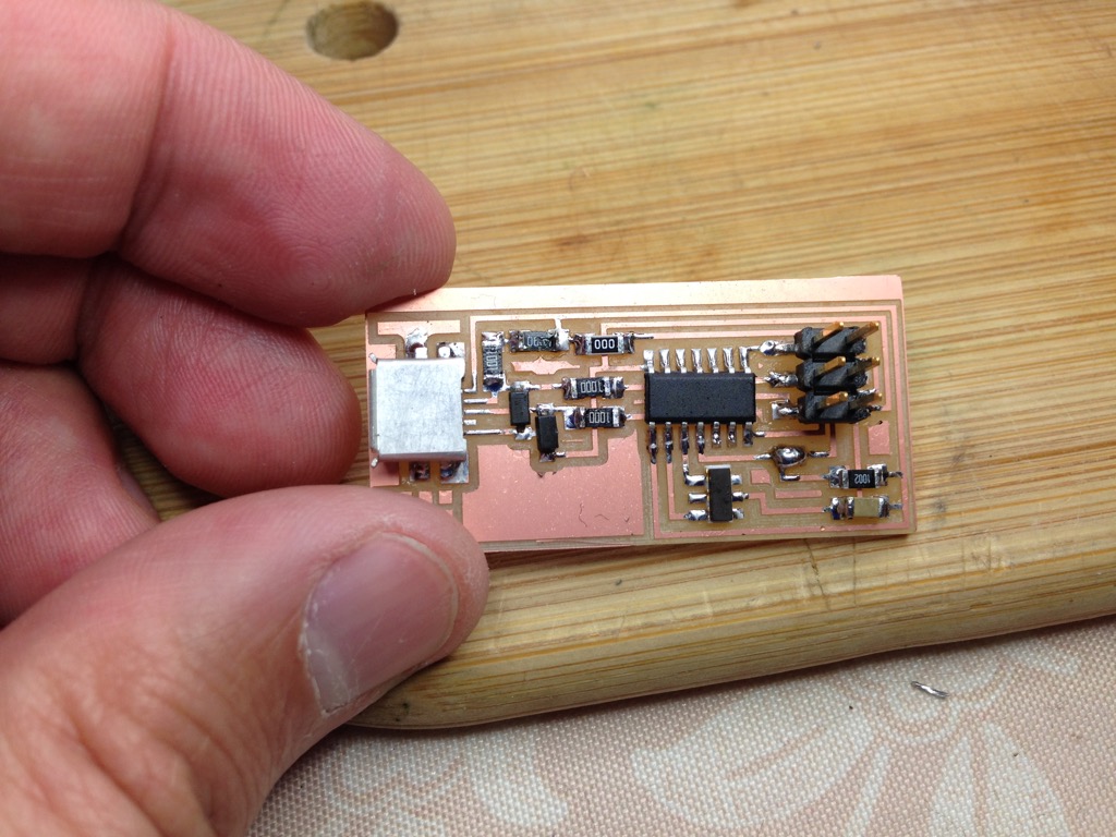
(just because of thickness of standard PCB..). Here is the board.

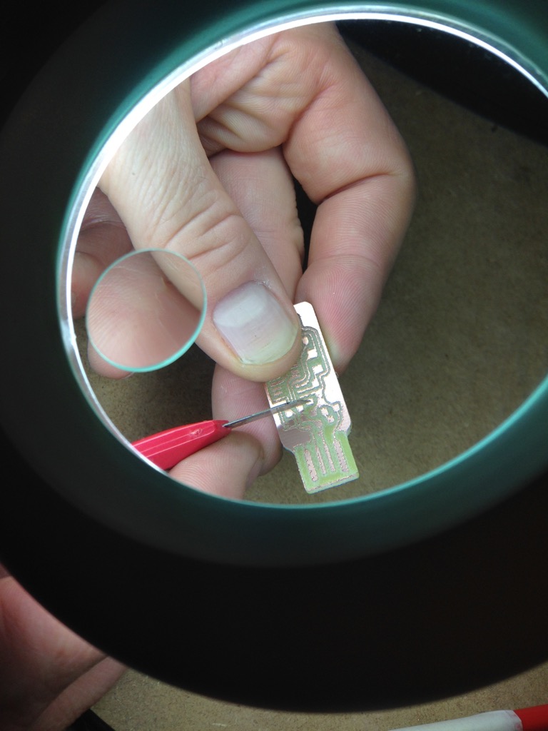
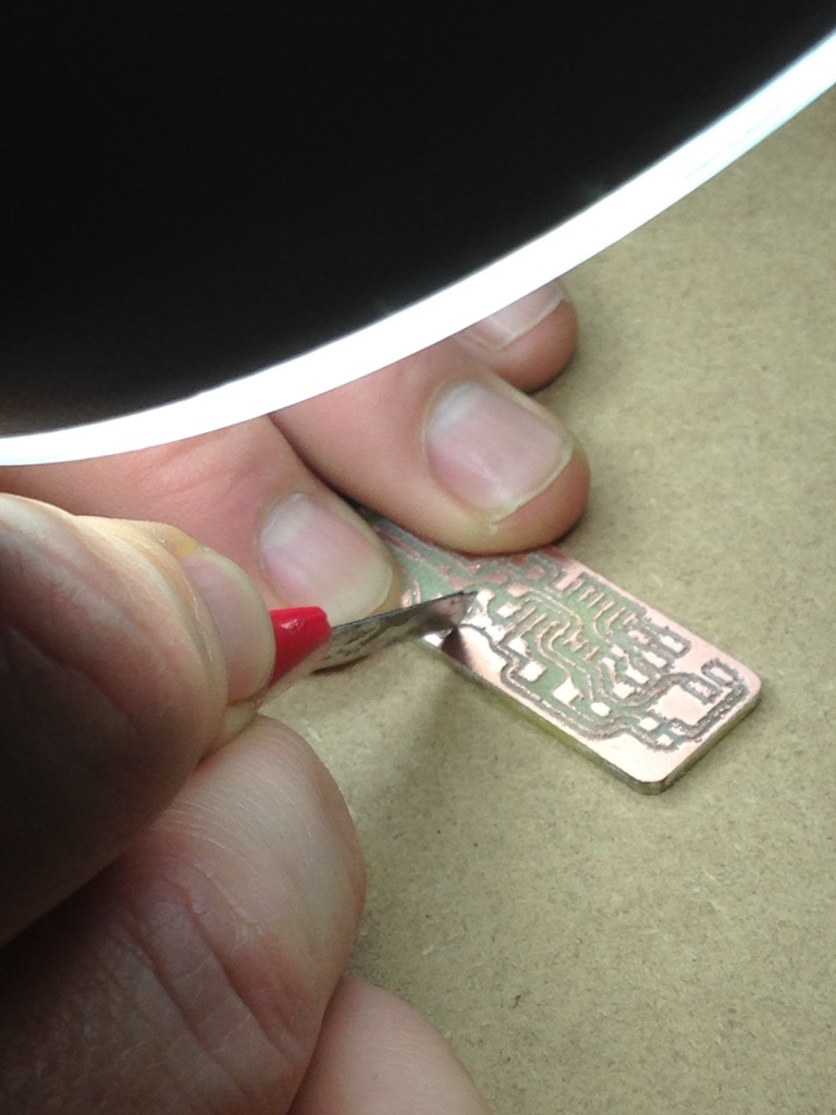
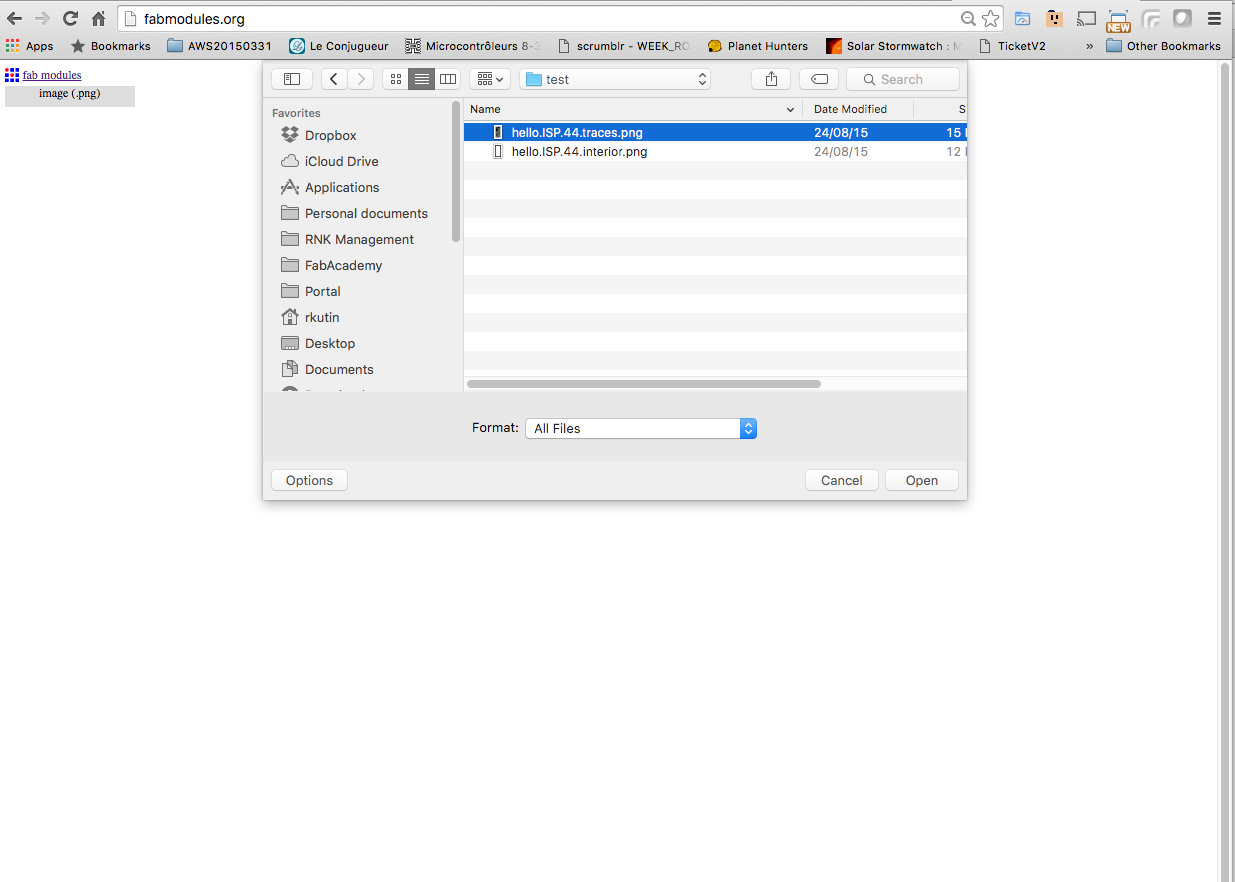
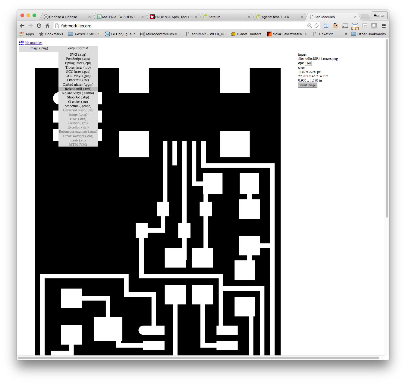
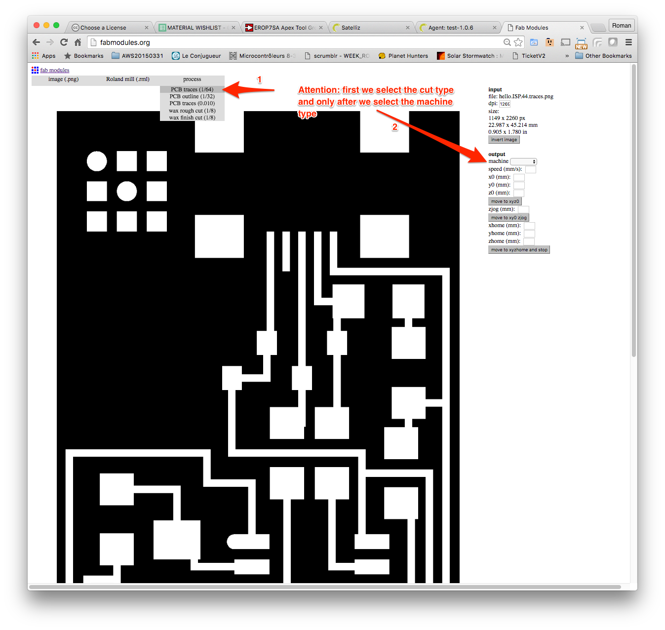
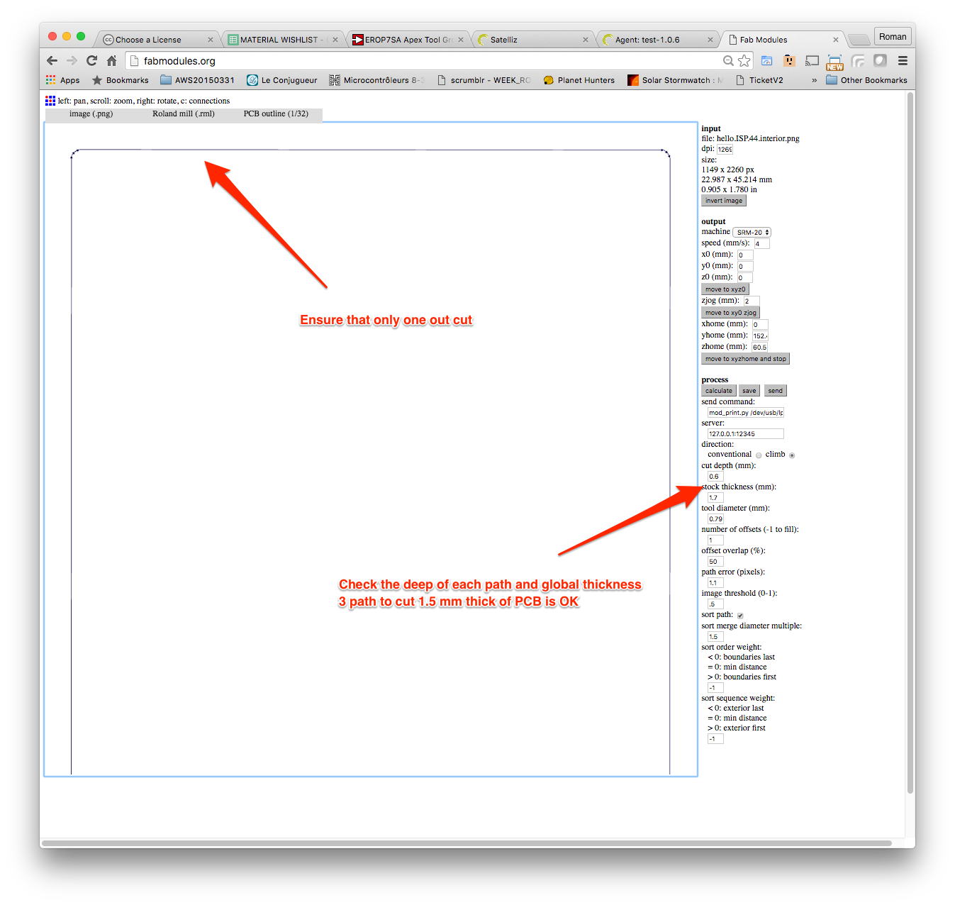
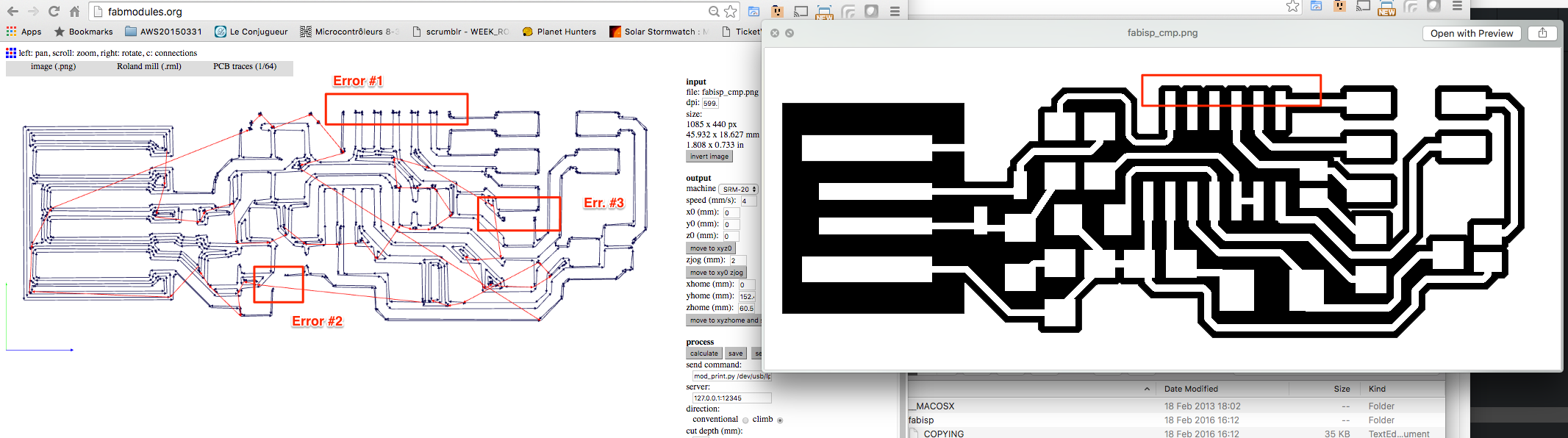
In this step I will not concentrate attention on cutting PCB using the Roland machine - it is explained few images above, but I will more explain the rest of process. Production and programming.

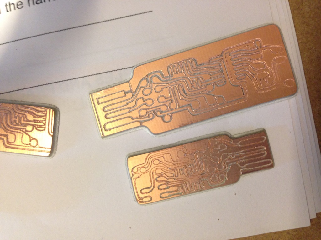
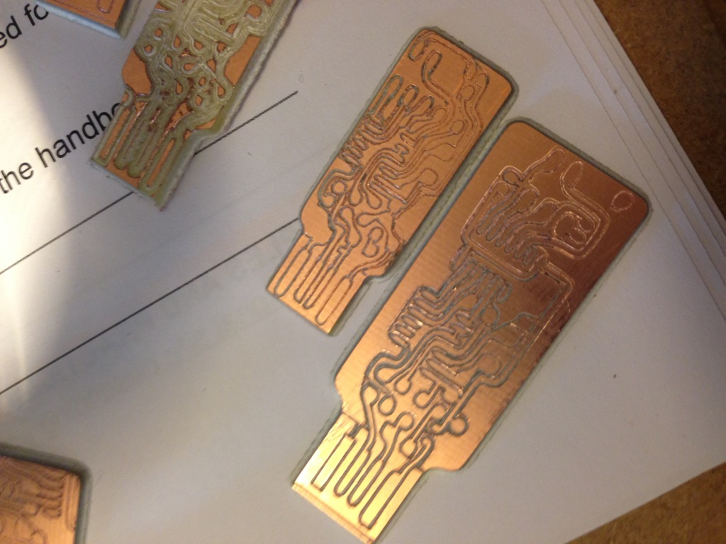
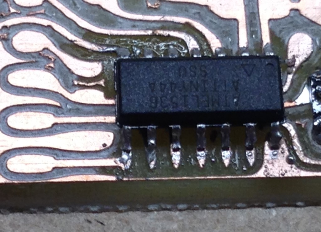
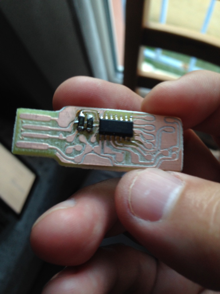
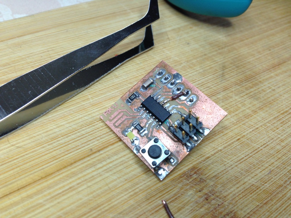
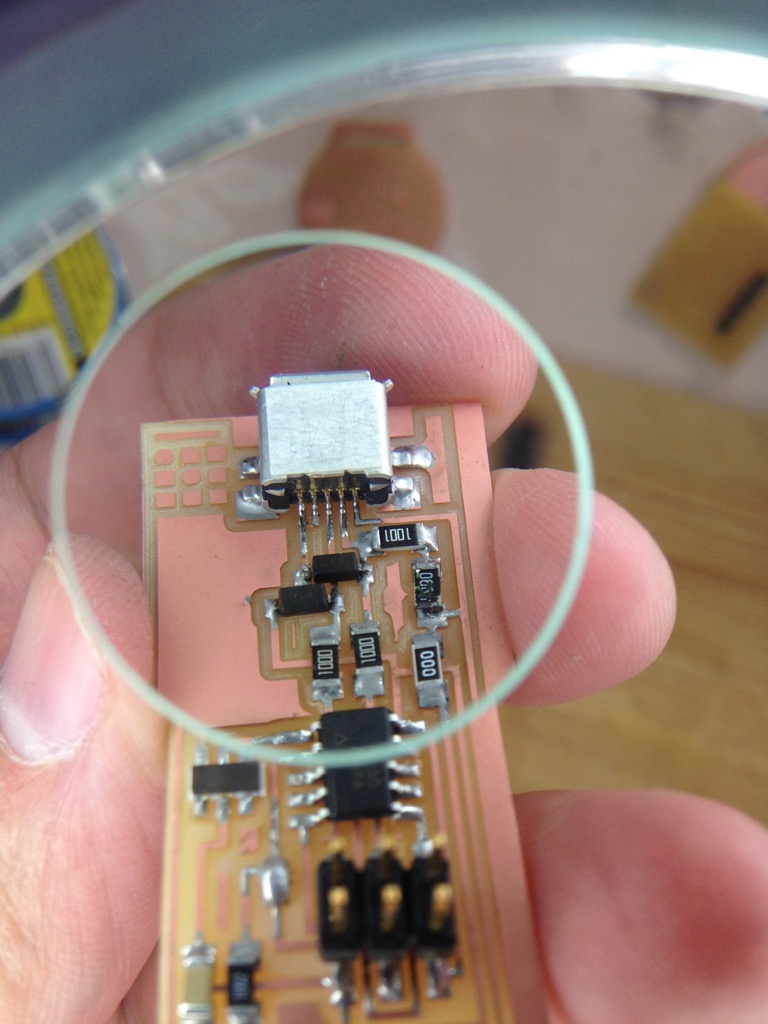
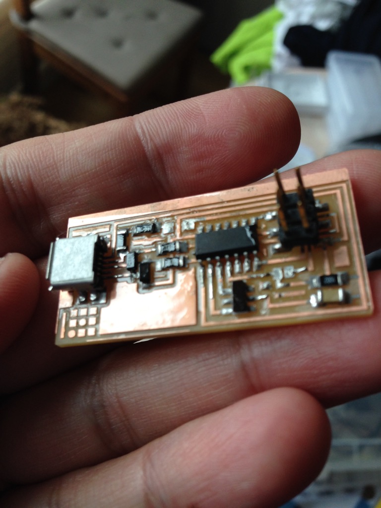
First - my first try ot FabISP is look very bad, beacuse I used the Flux during the soldering and I did not cleaned it. Now I will be smarter. Here is the bad result fabisp..

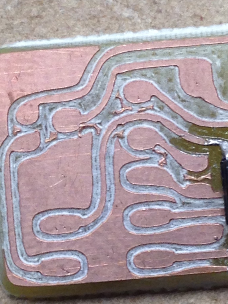
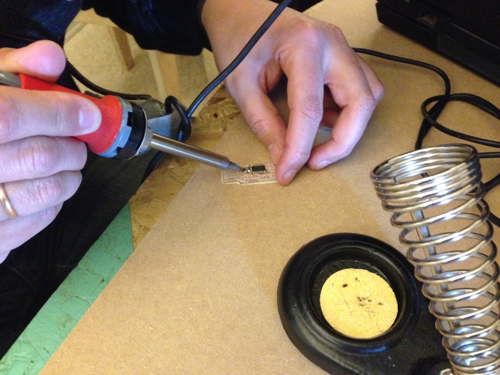
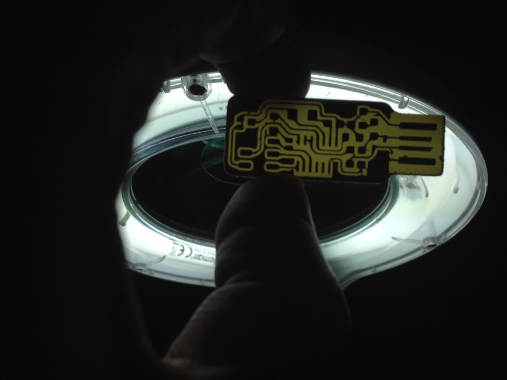
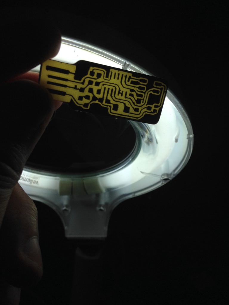
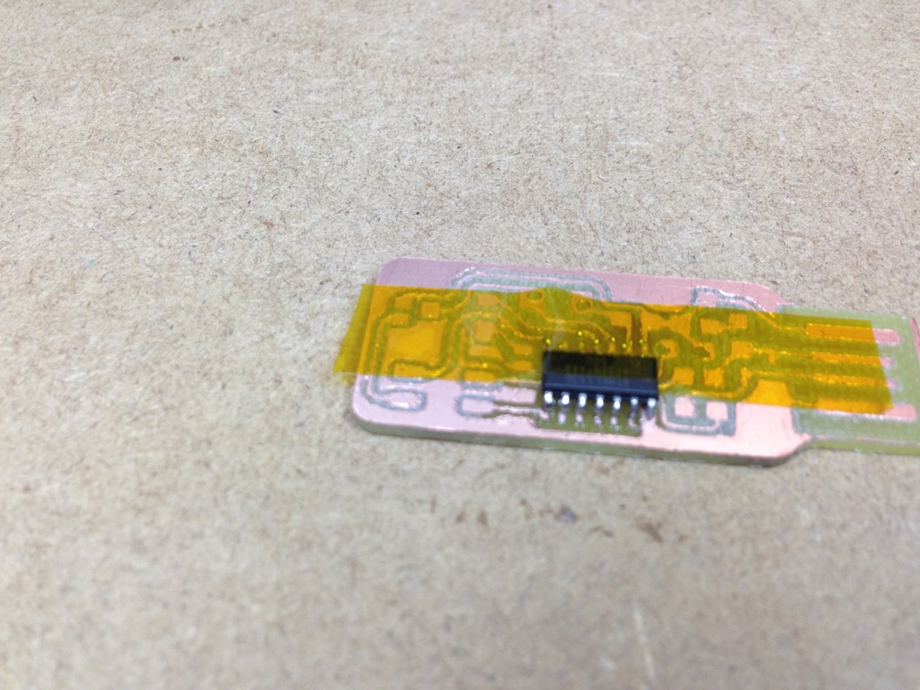
Let do smarter and do it well this time. So I did soldering using the standard method. (in fact after the test I found that attiny was soldered in inverse and it was killed by 5V - so I resoldered it by using airgun - and it still looks good. And it was difficult to take a photo by myself when I did worked with airgun.. So just resulted photos)


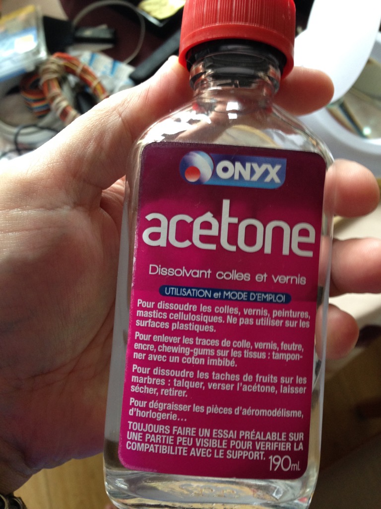
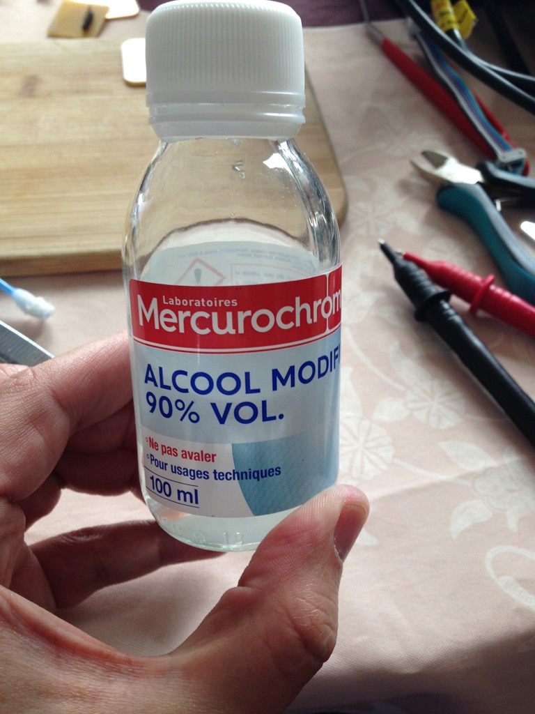
Then I did directly cleaning by using following products. (Acetone, to clean-up the flux, and acohol 90% to clean up acetone.) Below are the photos of both products.

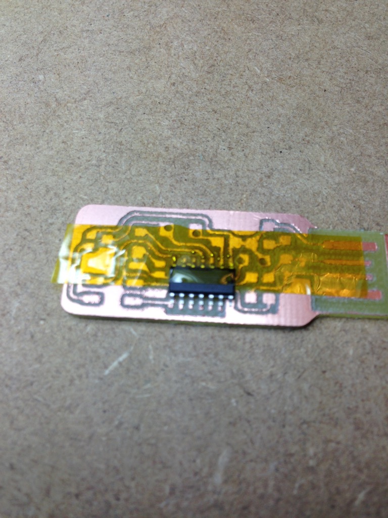
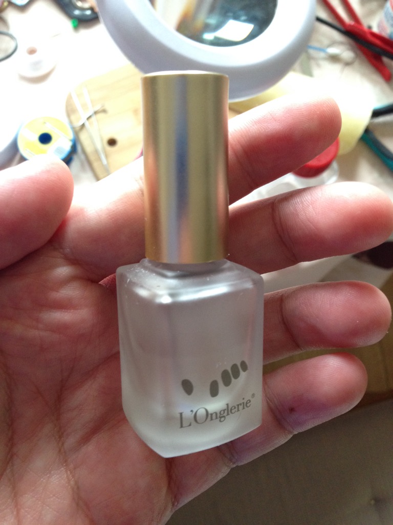
After this I pass my programming tests (I will talk about this later), and when I am ok with programmint - for protection I added "nail polish" over the cart. This wil permit protect cart from corrosion, from eventual water and grace. So here you will see the product I used and result of this processing.

Be careful, in case of required re-soldering - better to clean up by acetone before.

Programming for the FabISP

Now let pass to important phase of programming the Fab ISP.

During this phase we need to compile C-code to processor instruction, transfer them to the chip attiny and also we need to configure chip to work in defined environement (fuses).

Let download firmware and process it.

Firmware is available from the documentation page of selected FabISP. We need to unzip it to working folder. Then we will need some applications to process. If you are using Mac OS X - the simplest way to prepare environement (for the beginning of the 2016 ;-) ) is the homebrew. Follow the instruction from Homebrew site to install it. Then we will need to install everything around AVR microcontroller programming (at least the minimal part).
- avrdude: Is the application that permit you to communicate with your controler
- avr-libc: Pack of tools required to compile c-code to avr instructions

To install them use following commands:
$ brew install avrdude
This will permit you install the avrdude app
$ brew tap osx-cross/avr
$ brew install avr-libc
Deployment may take some time - just be patient.

Also for programming the FabISP you need to have another ISP programmer... If you do not have it - you can use Arduino as ISP (you can find many instruction about it). In my case I have one USBASP key - so I will use it.

When everithing is installed - we need to check if our ISP key may read data from just soldered FabISP. For this we need connect our USBASP key FabISP using the 6pins ISP header, (ground to ground, vcc to vcc and so on...). Then we need connect USBASP to our computer and let try to execute following command:

$ avrdude -c usbasp -p attiny44 -P usb -U flash:r:test.hex:i

avrdude: warning: cannot set sck period. please check for usbasp firmware update.
avrdude: error: program enable: target doesn't answer. 1
avrdude: initialization failed, rc=-1
         Double check connections and try again, or use -F to override
         this check.


avrdude done.  Thank you.
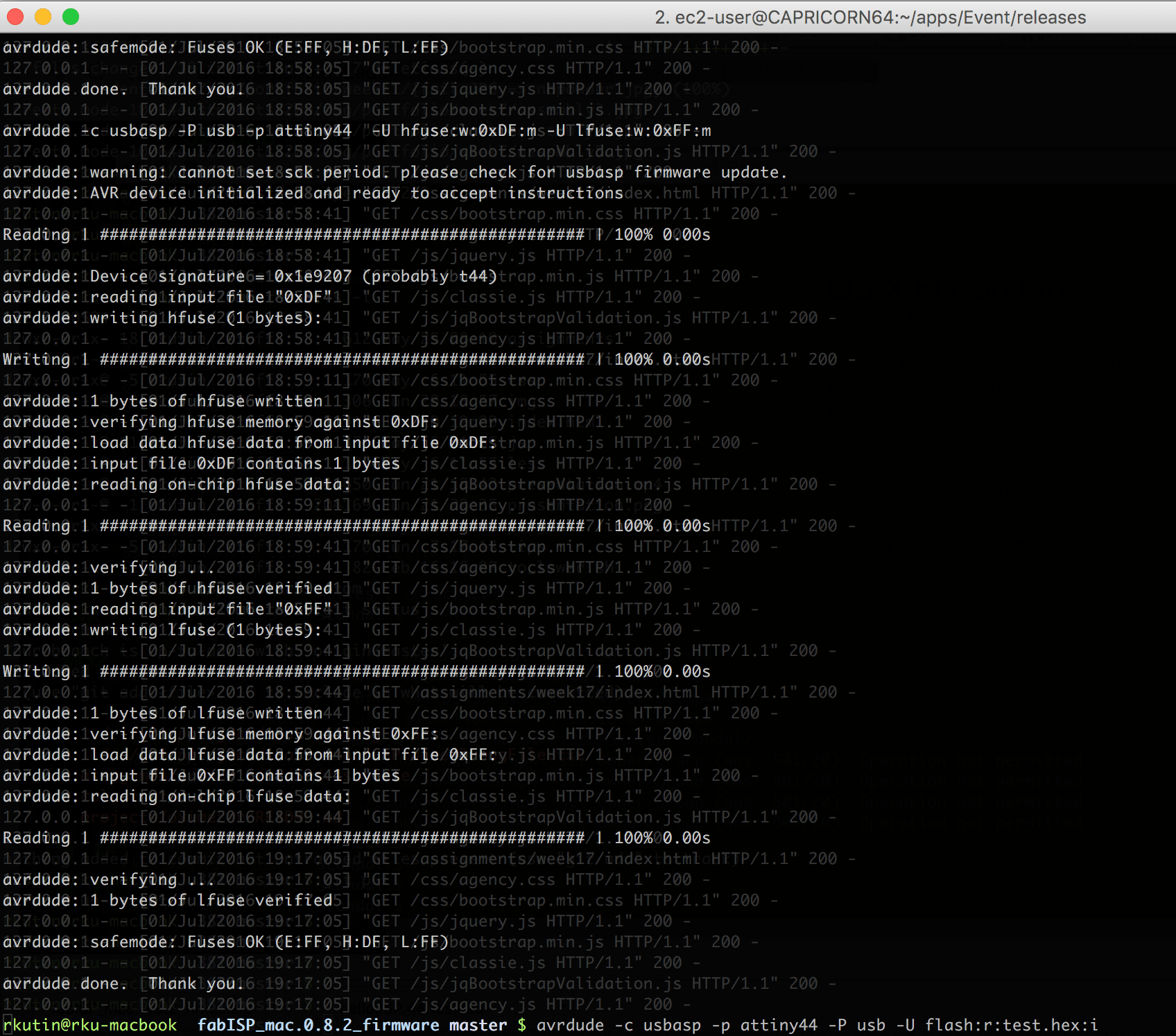
/// Here is example if somethig goes wrong and you need to check your connection and soldering
$ avrdude -c usbasp -p attiny44 -P usb -U flash:r:test.hex:i

avrdude: warning: cannot set sck period. please check for usbasp firmware update.
avrdude: AVR device initialized and ready to accept instructions

Reading | ################################################## | 100% 0.00s

avrdude: Device signature = 0x1e9207 (probably t44)
avrdude: reading flash memory:

Reading | ################################################## | 100% 2.10s

avrdude: Flash is empty, resulting file has no contents.
avrdude: writing output file "test.hex"

avrdude: safemode: Fuses OK (E:FF, H:DF, L:62)

avrdude done.  Thank you.
                      

If everything goes ok - you will see the progress bars of reading data from the chip. In fact the command above ask avrdude to read code curently written on the AVR chip and store it to local file test.hex. As the chip is empty now - file will looks also empty

$ cat test.hex
:00000001FF
$

Now when everything goes well - we will compile and put our program to our FabISP programmer. For this we unzip downloaded firmware and we modify our Makefile. In the first part of the file - we can see definitions that we need align.
- F_CPU - frequency of soldered crystal (20000000 is 20MHz crystal)
- AVRDUDE = avrdude -c usbasp -P usb -p $(DEVICE) # edit this line for your programmer - need to contain correct programmer name and correct port (after the -c and -P characters in this line).
So at the end the first lines of your files will looks like:

DEVICE  = attiny44
#F_CPU   = 12000000	# edit this line for crystal speed, in Hz
F_CPU   = 20000000	# edit this line for crystal speed, in Hz
FUSE_L  = 0xFF
FUSE_H  = 0xDF
#AVRDUDE = avrdude -c usbtiny -p $(DEVICE) # edit this line for your programmer
AVRDUDE = avrdude -c usbasp -P usb -p $(DEVICE) # edit this line for your programmer

Now we need to compile and upload code. For this you use command "make"

$ make
This Makefile has no default rule. Use one of the following:
make hex ....... to build main.hex
make program ... to flash fuses and firmware
make fuse ...... to flash the fuses
make flash ..... to flash the firmware (use this on metaboard)
make clean ..... to delete objects and hex file
$
                      
As you can see just make commands give us help how it should be used. First of all we need to generate .hex file (compile c-code to controller commands)
$ make hex
avr-gcc -Wall -Os -DF_CPU=20000000	 -Iusbdrv -I. -DDEBUG_LEVEL=0 -mmcu=attiny44 -c usbdrv/usbdrv.c -o usbdrv/usbdrv.o
avr-gcc -Wall -Os -DF_CPU=20000000	 -Iusbdrv -I. -DDEBUG_LEVEL=0 -mmcu=attiny44 -x assembler-with-cpp -c usbdrv/usbdrvasm.S -o usbdrv/usbdrvasm.o
avr-gcc -Wall -Os -DF_CPU=20000000	 -Iusbdrv -I. -DDEBUG_LEVEL=0 -mmcu=attiny44 -c usbdrv/oddebug.c -o usbdrv/oddebug.o
avr-gcc -Wall -Os -DF_CPU=20000000	 -Iusbdrv -I. -DDEBUG_LEVEL=0 -mmcu=attiny44 -c main.c -o main.o
main.c:88:13: warning: always_inline function might not be inlinable [-Wattributes]
 static void delay ( void )
             ^
avr-gcc -Wall -Os -DF_CPU=20000000	 -Iusbdrv -I. -DDEBUG_LEVEL=0 -mmcu=attiny44 -o main.elf usbdrv/usbdrv.o usbdrv/usbdrvasm.o usbdrv/oddebug.o main.o
rm -f main.hex main.eep.hex
avr-objcopy -j .text -j .data -O ihex main.elf main.hex
avr-size main.hex
   text	   data	    bss	    dec	    hex	filename
      0	   2002	      0	   2002	    7d2	main.hex
$
                        
This generate main.hex file - that we can see in folder (it contain instructions for the chip.)
$ ls -l main.hex
-rw-r--r--  1 me  staff  5655 Jul  3 18:53 main.hex
$ head -10 main.hex
:100000002BC06EC144C043C042C041C040C03FC0CD
:100010003EC03DC03CC03BC03AC039C038C037C00C
:1000200036C009021200010100801409040000001A
:10003000FF00000012011001FF00000881179F0C53
:100040000401000200010E03460061006200490045
:10005000530050000403090411241FBECFE5D1E072
:10006000DEBFCDBF10E0A0E6B0E0E0EDF7E002C0FB
:1000700005900D92A236B107D9F720E0A2E6B0E0D4
:1000800001C01D92A53AB207E1F785D39FC3B8CF4F
:10009000CF93DF9360918B00635067FD9AC080918E
$
                        
Now let configure chip (make fuse). Below I used images instead of text to reduce space, and I can not reproduce them again as they were already fused and programmed. As result of $ make fuse program - will configured fuses and our chip start to use the external crystal on 20 MHz

Now let push program code (already generated main.hex file) to the chip. For this we use $ make program command.

Now if you will re-executed avrdude command in same way as we did at the beginning to read code from the controller - the text.hex file will contain much more lines then before. So everything goes well.

To check that your process is passed correctly - you do in mac os x -> About this mac -> System report (using the main menu) and you go to USB section. There you must see connected FabISP :-)
In fact FabISP program use the virtual USB code that permit to AVR contoller communicate with computer emulating the USB interface - so it is really becomes one USB device. Here is how it looks like:

Now you must follow the documentation of FabISP producing page and unsolder 2 jumpers (JP1 and JP2) - they are put on place to permit you re-programm your FabISP, then they are not useful. And after this you use the nail polish as I described above to protect your FabISP. You can also later produce a box for it - it becomes very useful tool.