Assignment 6
Задание 6
(2ND EVALUATION EDITION) In which I use Sprint Layout to make the quickest design ever
В которой я становлюсь лучше в фрезеровке, но пайка всё ещё остаётся проблемой
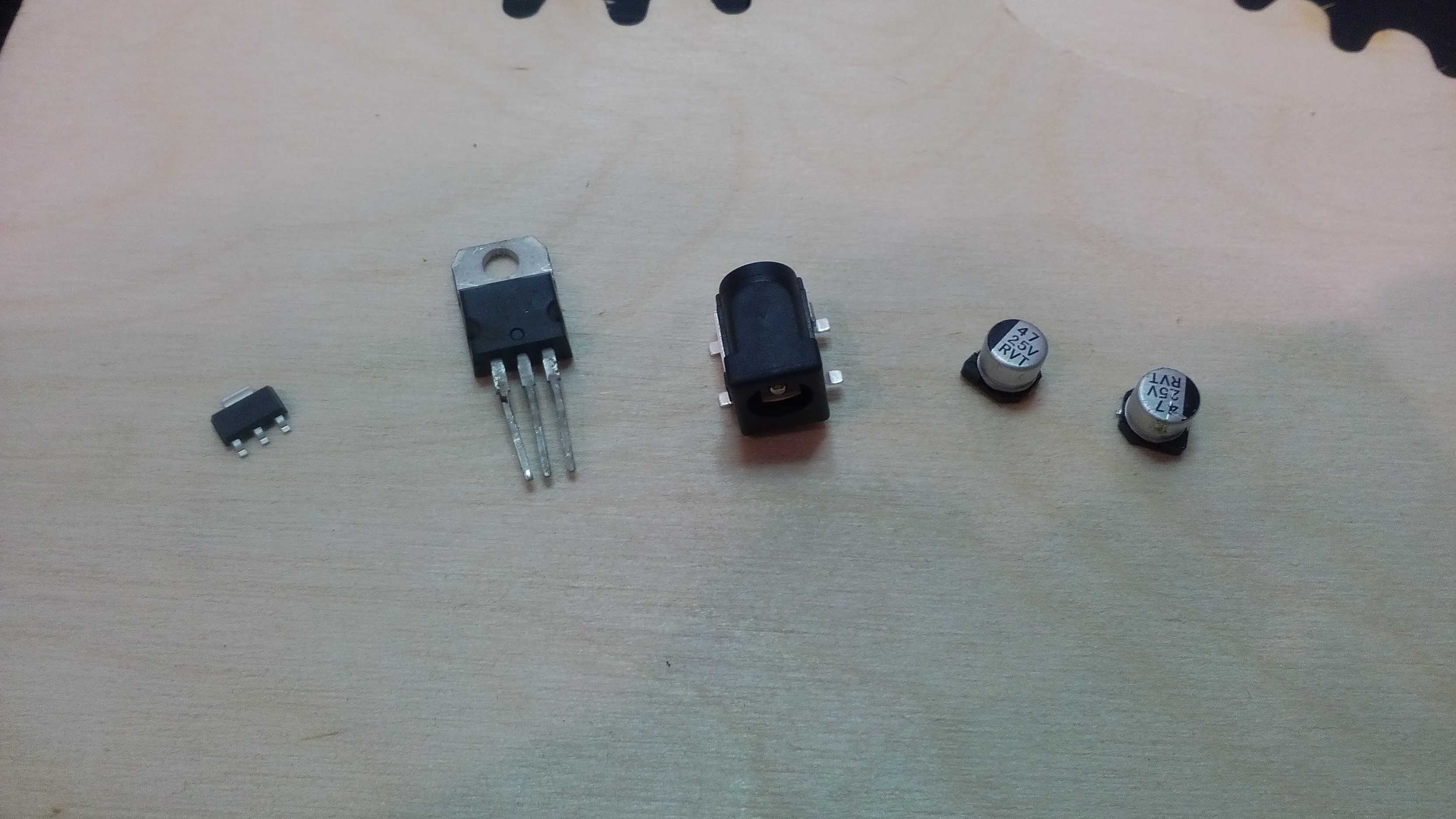
My task for this assignment would be to design a power supply part for my future pcbs which would include voltage 12V to 5V converter (L7805) with assisting capacitors (47uF, 25V), transistor (PBC69) to be a key for some 12V component as LED stripe and it'll be extremely useful in my future projects.
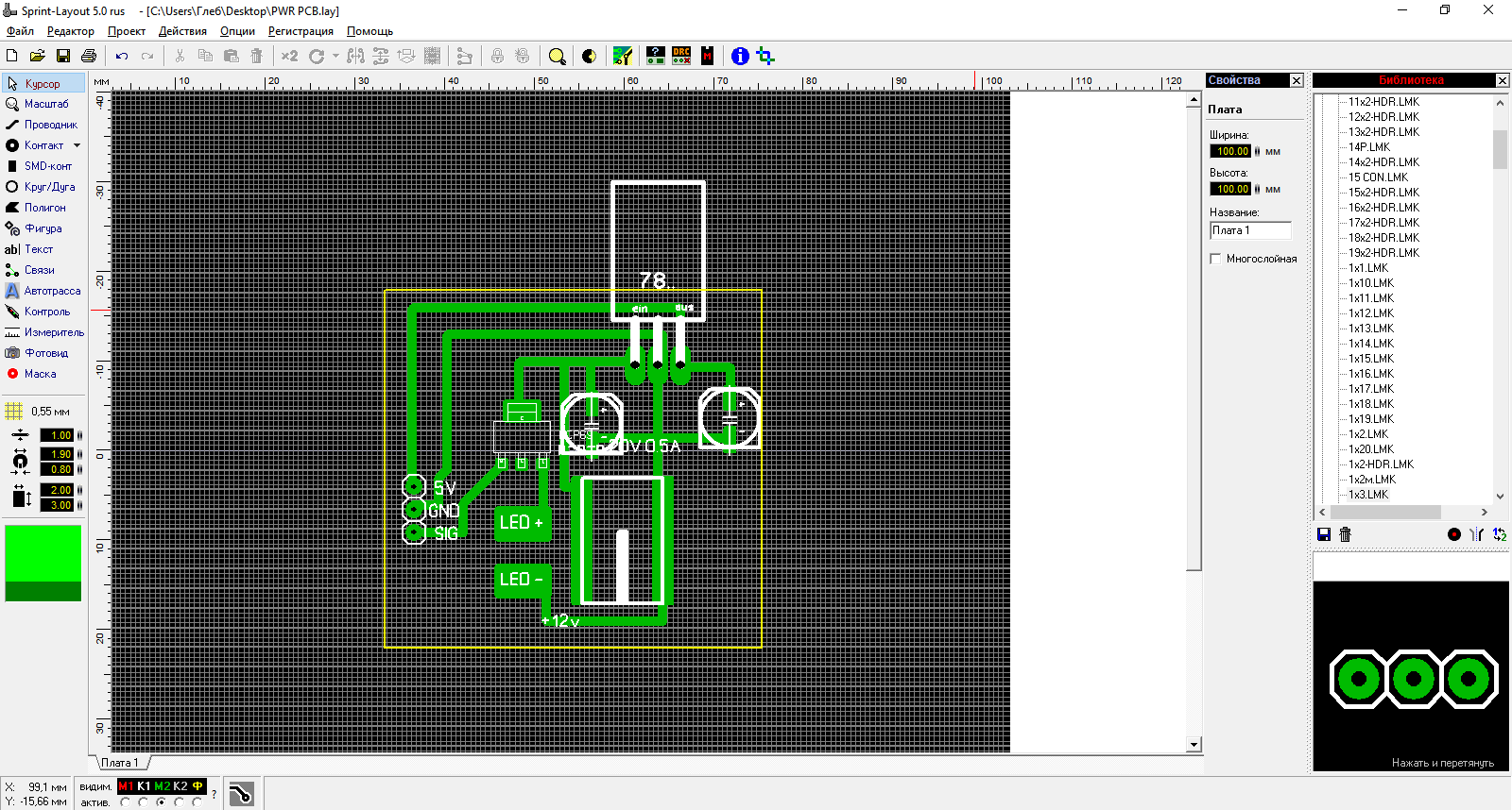
In every other assignment I use Eagle (even in this one, pre-evaluation edition) but here I'd like to design the pcb with another tool - Sprint Layout. It is an extremely simple program and is very useful when you have a simple task and lack of time.
This is why I love this program: it is easy as abc. In this videos I literaly design a pcb in 10 minutes or something: make library components, make traces, export a layout. Sure, it misses schematic part of Eagle and guiding traces to connect different elements but speed of designing is very satisfying.
Little commentary on different operations: drawing traces and elements consists of a small amount operations such as drawing a trace of different configuration (length, angle, width, number of nodes); smd pad (width x length); circles (inner and outer diameter); polygons - infilled contour of traces; holes (different hole diameter and pad parameters).
Learn more about milling pcbs in week 4 assignment
here's and actual tutorial for Sprint Layout
Final thoughts
Even though this program is very easy, it's even easier to get confused without electrical scheme which is obligatory in Eagle so if I'd have a serious task to accomplish, I'd totaly use Eagle instead. Also I redesigned and reassembled pre-evaluation board from this assignment.
Downloads
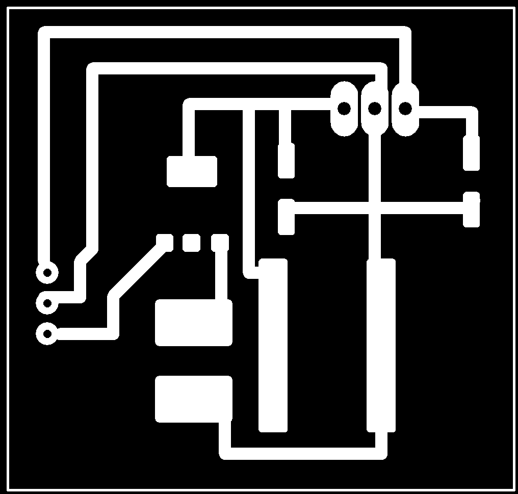
Ele-Design.rar Includes Sprint Layout file (PWR BRD.LAY) for the pcb I designed, .png file for producing it and Eagle files for Echo board redesign (Push.brd, Push.sch)
Redesigned pcb from pre-evaluation; files to download are included in assignment archive
In which I do a better milling but soldering still remains uneasy
Making my own Redesigning a pcb
Делаю свою Переделываю готовую плату
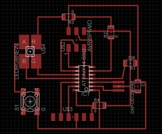
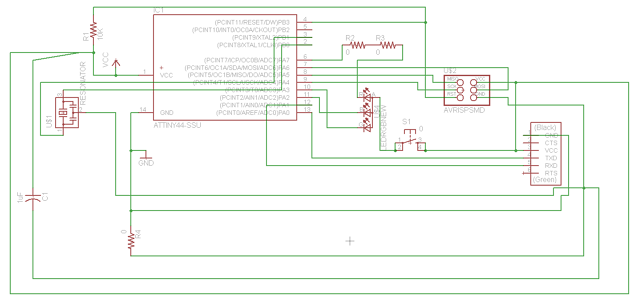
This week is all about designing tools for making pcbs and electronic schemes, and I chose hello.ftdi.44.echo board to redesign. As for me, I tried using Proteus and Sprint-layout for my previous projects: electronic alarm with keypad and breath repeater project but in the first case it was used only as a schematic-design tool with an ability to test the controller programm an for btreath repeater I just put holes and traces mindlessly.
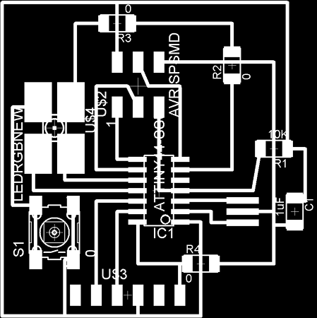
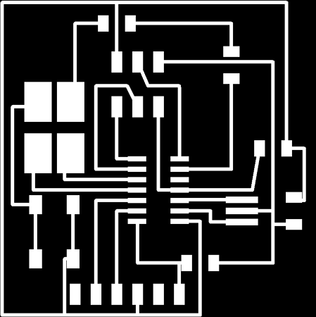
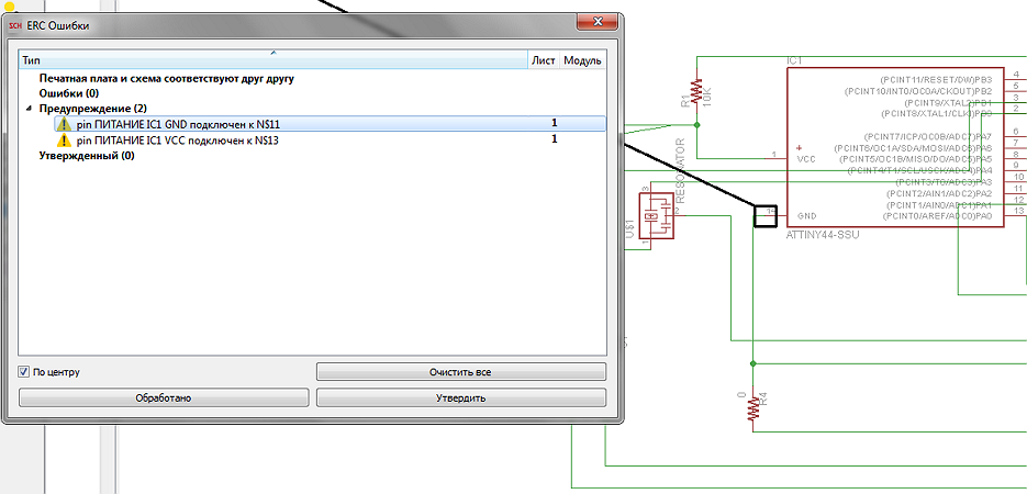
Now, it's Eagle time! First of all, I found a library with all the components I need so I won't have to reinvent the bicycle. And then - action. Actually, it turned out to quite easy (because all I had to do is add components from library and connect them with wires) but I couldn't get rid of an error saying that GND is connected with GND port of the controller and VCC is connected to VCC port. Well, that was weird. And then Dima told me that I have to put a VCC and AND symbols on a scheme and also connect them to controller ports but it doesn't effect the pcb whatsoever. Then, after all errors were solved, I got a bunch of places for electronic components on my pcb layer so I arranged them as I wanted to and connected glowing yellow lines with traces. Voila!
Also, to make it easier for me to export my pcb layout, I wrote a script for Eagle as in this instruction. Scheme, pcb layout and Eagle script are on the links below.
На этой неделе мне надо освоить программы для создания плат, и в качестве подопытного я выбрал hello.ftdi.44.echo board. Что касается меня, я раньше использовал Proteus и Sprint-layout в моих предыдущих проектах: сигнализация с клавиатурой и пповторитель дыхания но в первом случае я пользовался только редактором схем с возможностью тестирования программы контроллера, а для повторитля - просто бездумно расставлял отверстия и дорожки.
И вот теперь я принялся за Eagle. Перво-наперво я скачал библиотеку со всеми необходимыми компонентами, чтобы не изобретать велосипед. Теперь - к делу. Вообще, составлять схему казалось несложно (хотя бы потому, что мне надо было всего лишь раскидать компоненты по полю и соединить проводами в нужных местах), но я никак не мог побороть ошибку, которая говорила, что земля соединена с землёй на контроллере, а питание соединено с питанием контроллера. Но ведь так и должно быть, так? Позже Дима объяснил мне, что мне надо добавить символы VCC и AND на схему и соединить их с портами контроллера, что, кстати, никак не влияет на четрёж платы. Теперь, когда я разобрался с ошибками, я получил кучу посадочных мест под электронику, соединённых между собой жёлтыми линиями на слое с раскладкой платы, которые я расставил в нужном мне порядке проложил между ними дорожки платы. Вуаля!
Также, чтобы облегчить экспорт (не скрывать слои с заметками вручную), я написал скрипт для Eagle по этой инструкции. Схема, раскладка платы и скрипт для Eagle приведены ниже.
Exported without script -> exported with script
Экспортирую без скрипта -> экспортирую со скриптом
If you see this kind of error, you should probably add VCC and GND symbols
Если вы видете эту ошибку, попробуйте добавить символы VCC и GND на схему
EZ milling
Лёгкая фрезеровка
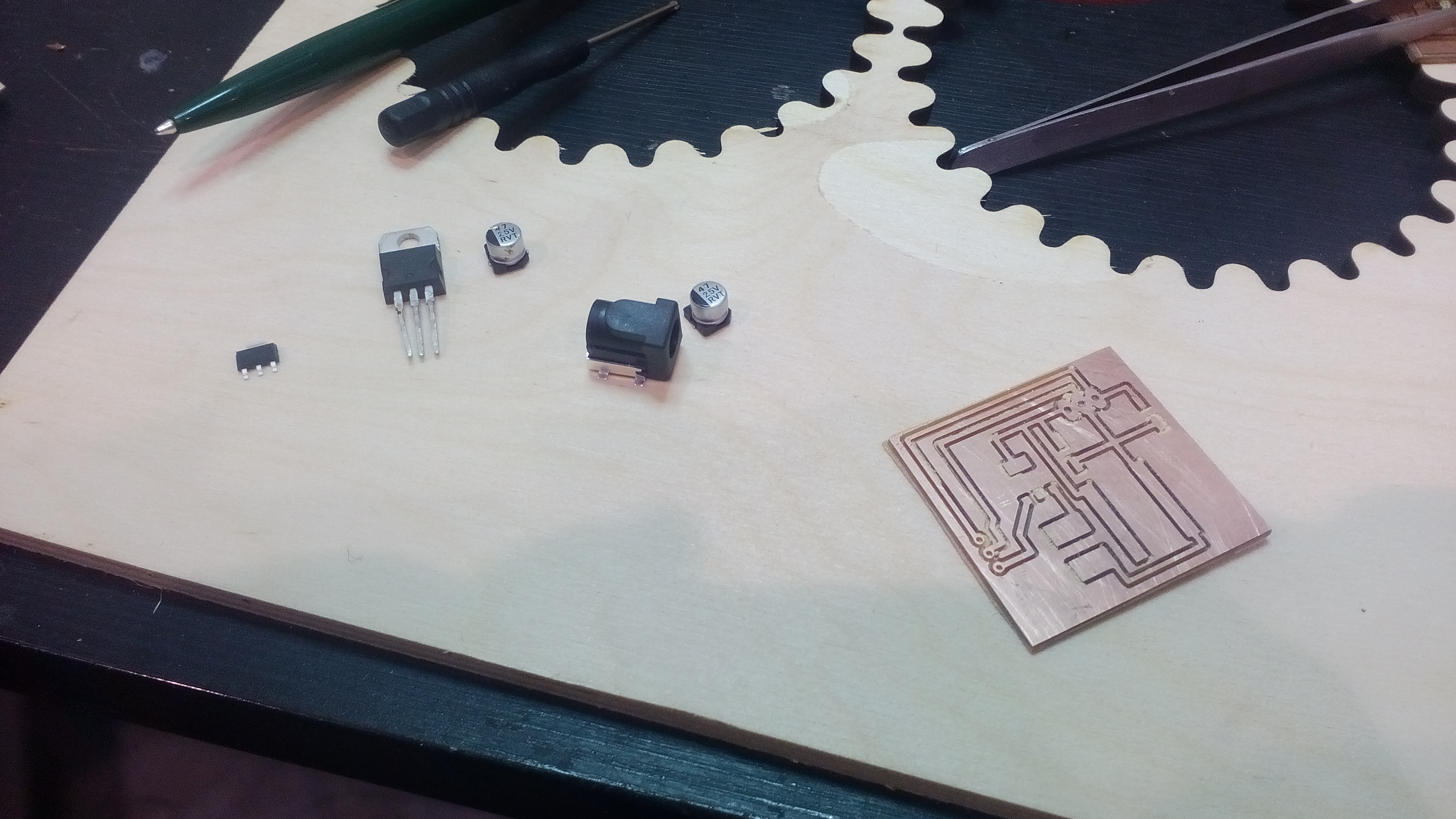
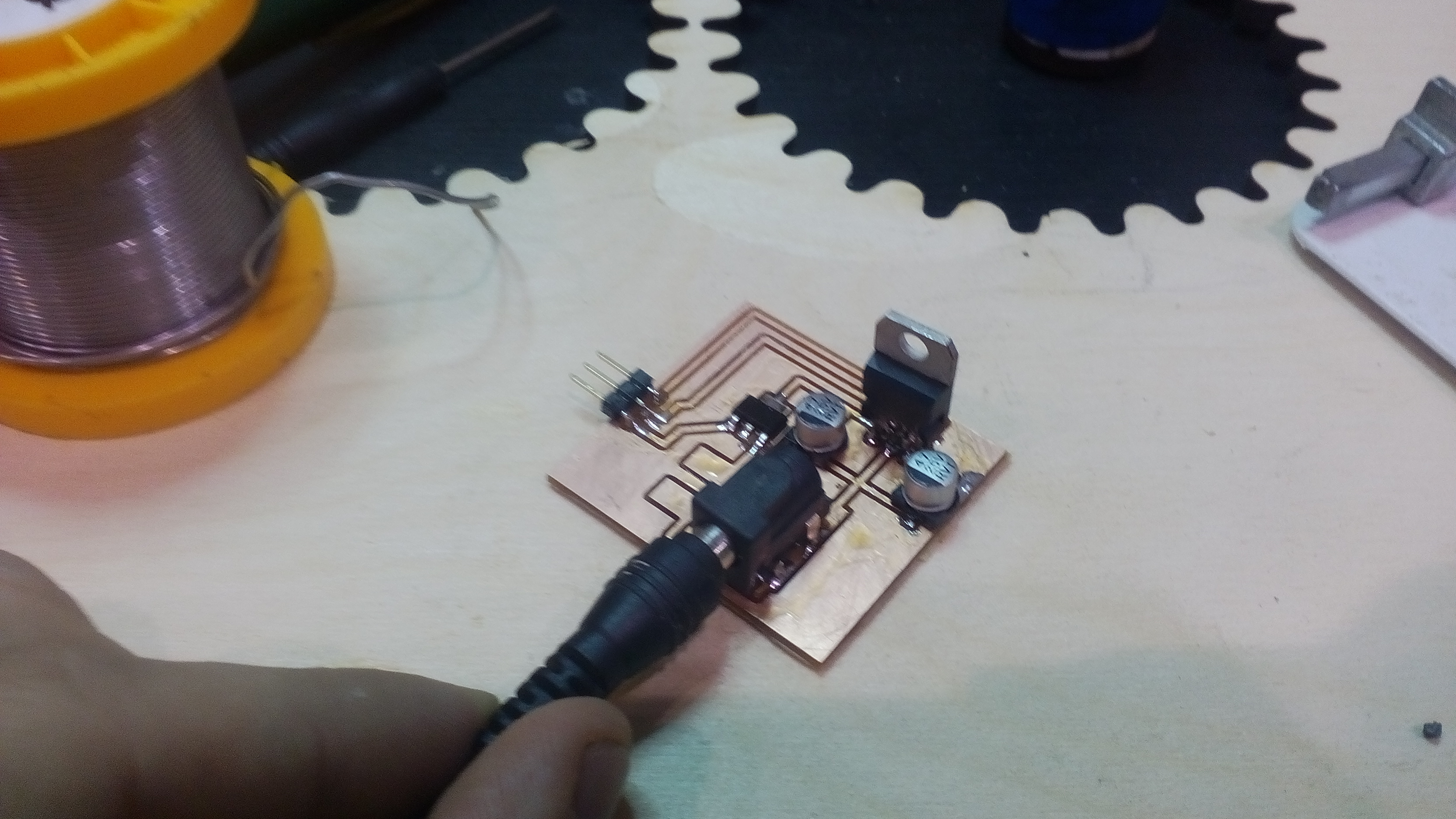
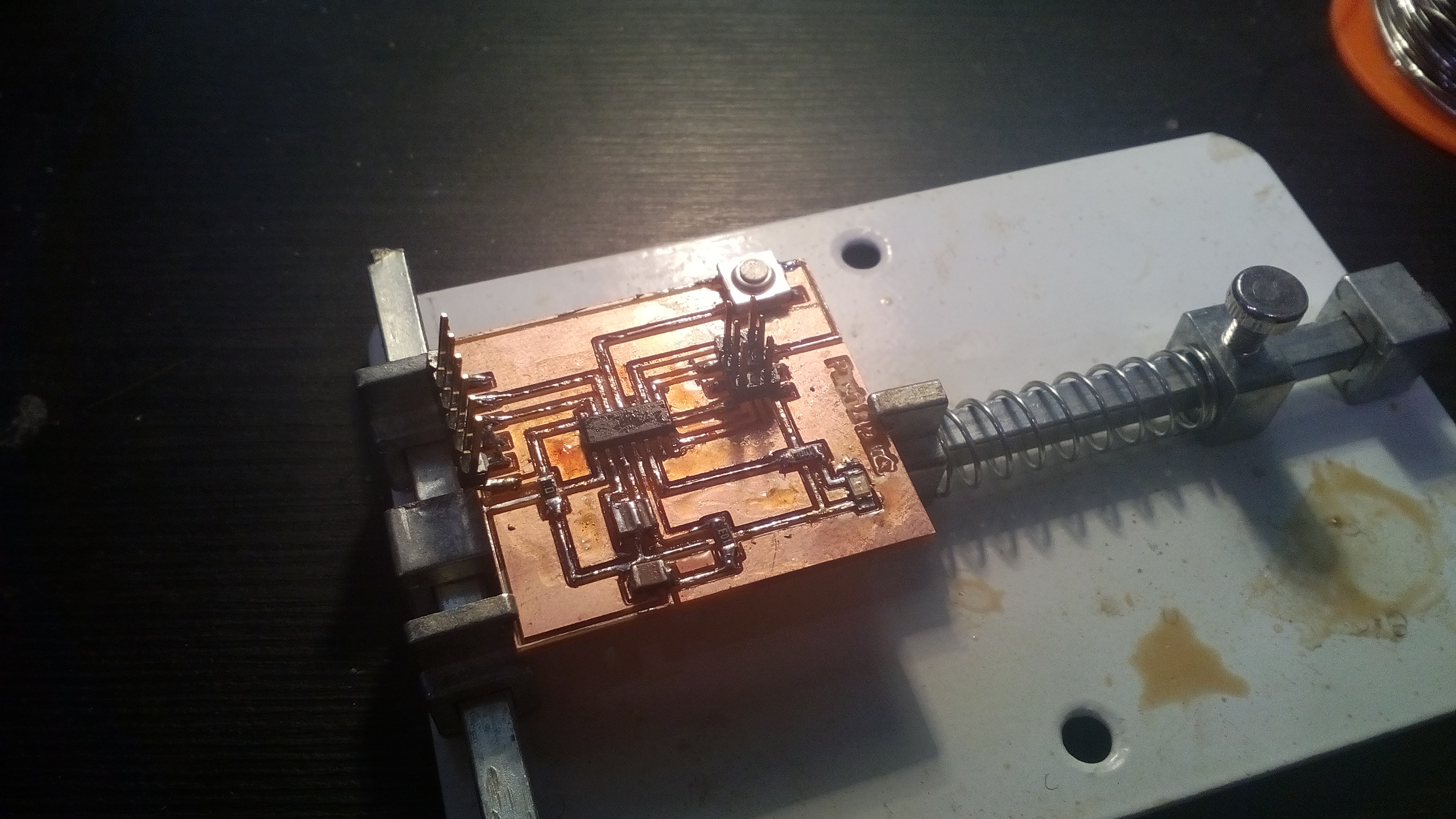
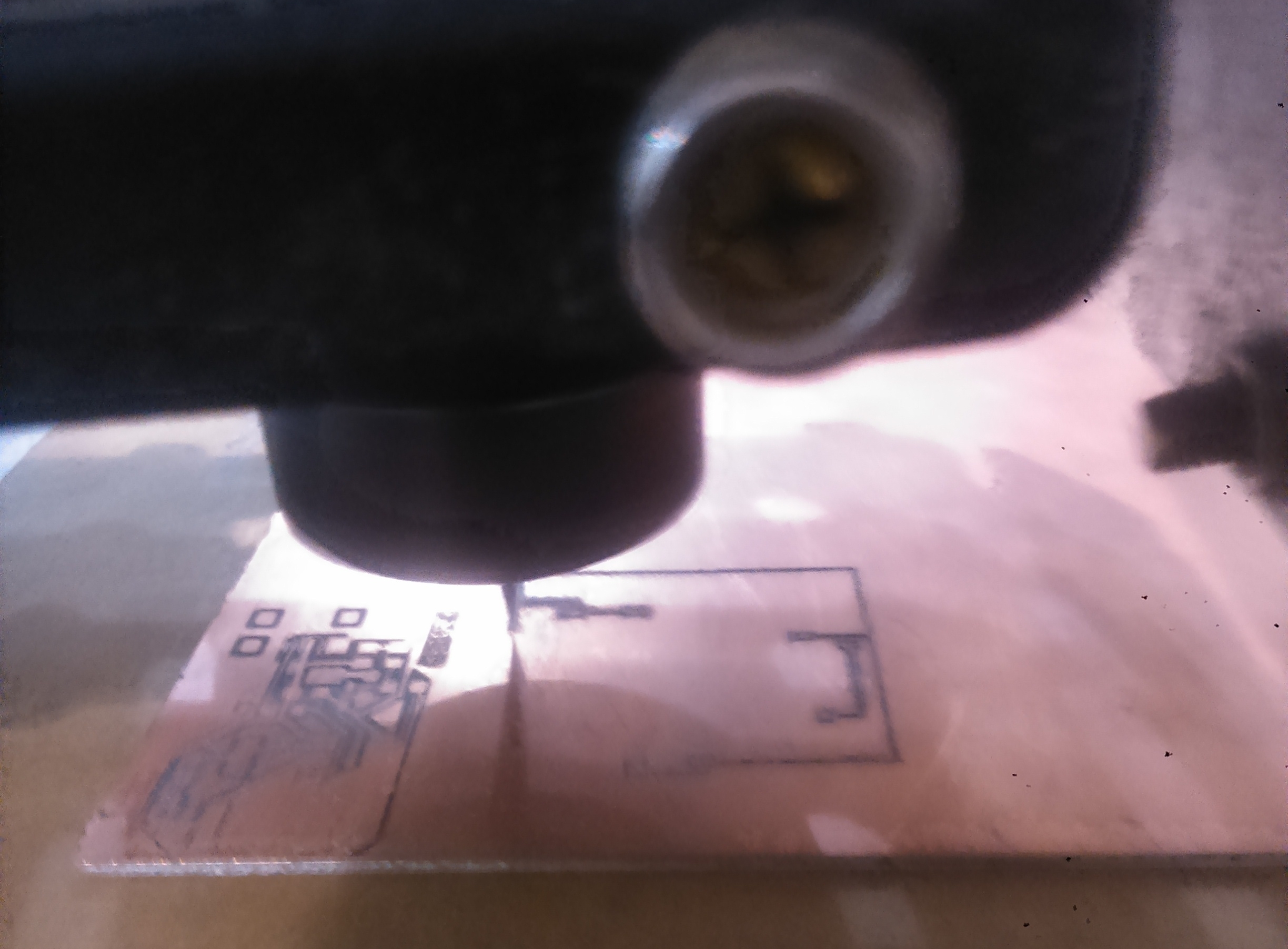
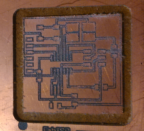
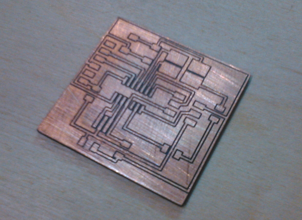
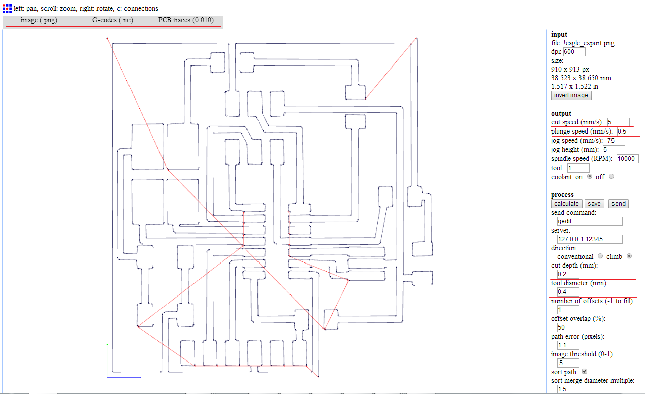
Well, that went okay. As in electronics production assignment, I used a double-sided sticky tape and a hardbord to make textolite hold still on my milling machine, K2, 0.4 mm mill to make traces and fabmodules to make a g-code. The one thing I changed - I made only one offset this time. After milling I sandpapered my pcb and I want to mention that it looks fabulous. I really like it. Here is g-code of my pcb.
Ну, лучше, чем ожидалось. Как и на четвёртой неделе, я использовал двустороннюю клейкую ленту и кусок двп, чтобы установить текстолит на столе фрезерного стнака K2, 0.4 мм фрезу, чтобы делать дорожки и fabmodules, чтобы сделать g-code. Единственное, что я поменял - сделал только один offset. После фрезеровки я прошёлся наждачкой по плате, и теперь она смотрится восхитительно, я очень доволен. Ниже приведён g-code для фрезеровки моей платы.
Soldering strikes back!
Пайка наносит ответный удар!
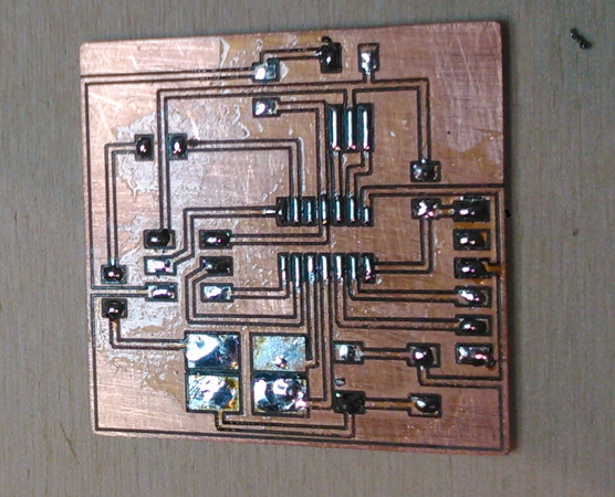
Everything was going pretty well till this point. A couple of times I made a shortcut with solder because spaces between traces was so small and also there was a whole pcb of unmilled copper to make shortcuts with. Point to etching - it leaves no extra copper. And as a result I had to redo my soldering very careful. Still, it's dirty because of liquid flux that I use.
До этого момента всё шло довольно неплохо. Пару раз я сделал короткое замыкание припоем, перелившимся на соседнюю дорожку и на "лишнюю" медь, оставшуюся от врезеровки, потому что выфрезерованное пространство было слишком малым. Очко травлению - остаются только дорожки и посадочные места, никакой лишней меди. В общем, мне пришлось переделывать всё очень осторожно. Но плата всё-таки получилась грязноватой из-за жидкого флюса, который я использовал.
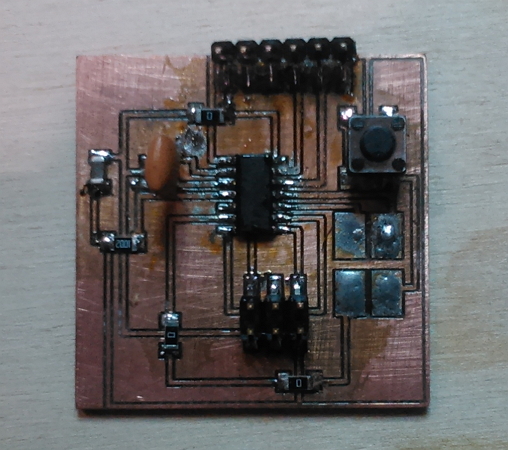
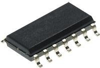
- Attiny44
- 20 MHz ceramic resonator (as we're cuttently waiting for our parcel with components, I had to use analog)
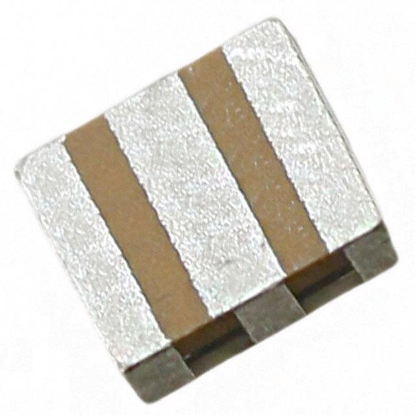
- 10K resistor SMD 1206
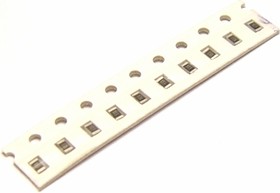
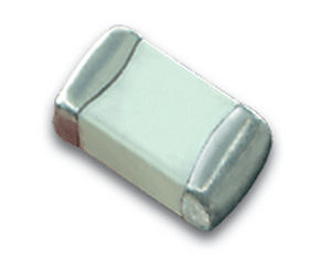
- 1uF capasitor SMD 1206
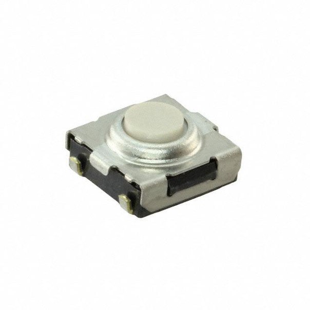
- SMD button
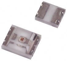
- SMD RGB Led
- 3x2 connector
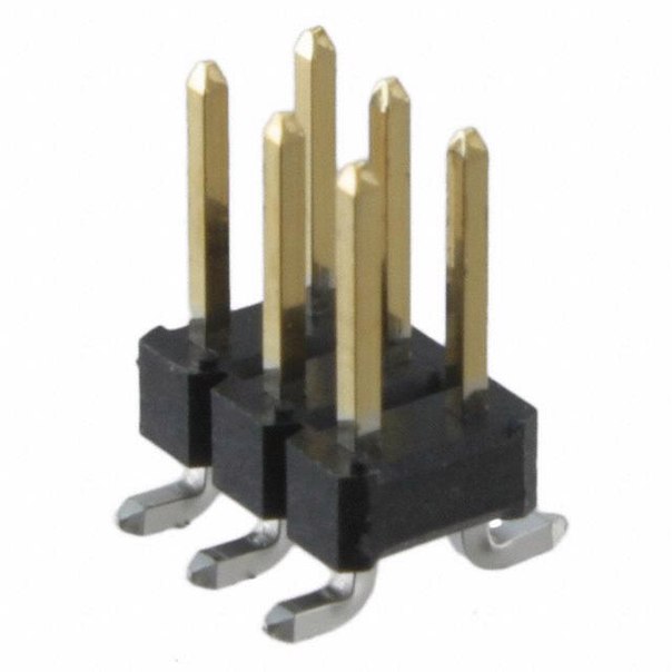
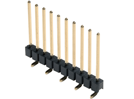
- 1x6 connector
- Attiny44
- Керамический резонатор 20 МГц (так как наши компоненты ещё не пришли, пришлось использовать аналог)
- 10KОм резистор SMD 1206
- 1мкФ конденсатор SMD 1206
- SMD кнопка
- SMD RGB светодиод
- 3x2 порт
- 1x6 порт