2016
Rudrapalsinh Solanki
Week-4
Electronics production
Assignment
1. Make the FabISP in-circuit programmer
2. Solder all the required components in the board.
I Decided to make a fabIsp and make it work with AVRISP programmer for do this exercise.
I wanted to learn and understand the working of FABISP.
So I designed a pcb with the attiny 45 and then see the working of the board.
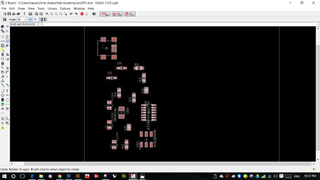
Now its turn to design the board in Eagle design and start working with it.
Steps involved are :
1. Design the board with the required components
2. Milling the board
2. Soldering the components
3. Programming of the board through Arduino
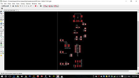
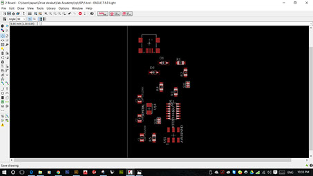
1. Design the board with the required components:
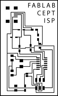
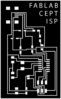

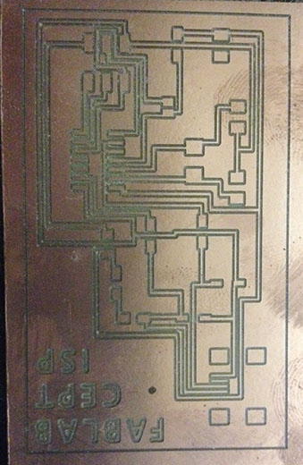
This the png created from the eagle now invert the image to get the final image
Png file download
Png file download
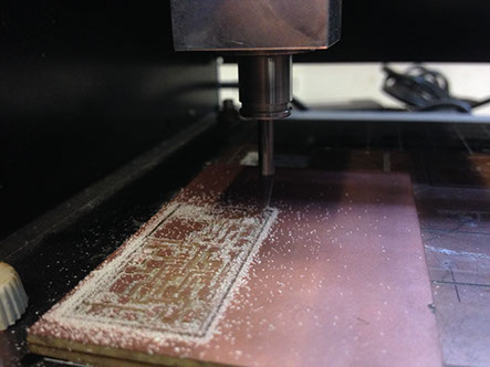
2. Milling of the board:
3. Soldering all the components on the board:
Board getting ready for soldering:
Board Ready after the soldering all the components and now ready to connect.
For more Details on soldering please see the bottom of the page
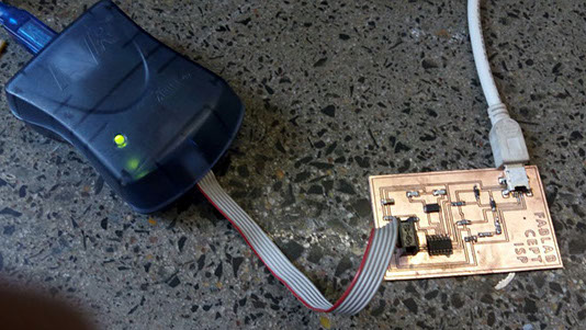
The board is connected to the computer and the green light of AVRISP shows successful connection.
For more Details of connection please see the bottom of the page
Board is now ready for programing through AVRISP
For more Details of programing please see the bottom of the page
I am new to the electronics. I had never worked with any of the electronics. I started making my own board. I downloaded the ready file for the hello ISP board from the Fab module inventory. The file looks something like this:
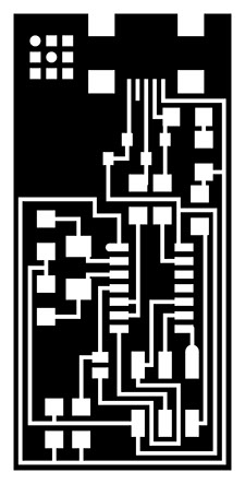

The cutting file for the hello ISP board. The file that I downloaded from the archive was a png file. The file contained all the traces for the paths of the circuit and also had the guides for the components that will be accembled on the board.
The other file that I downloaded was the file for the outer periphery of the circuit. This file has to mill on the machine after the main circuit is milled. This file is mainly used for cutting the board directly for mthe major circuiut board.
Components needed for the Hello ISP board:
Micro-controller
Crystal
USB connector
Ribbon connector
Zener diode
Jumper wire
Firmware
Resistors
Capacitors
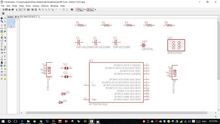
Circuit diagram for the board:

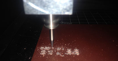
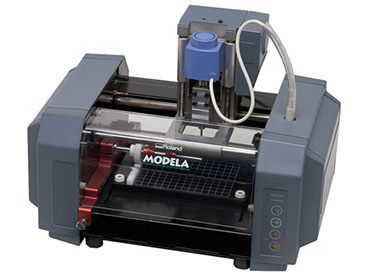
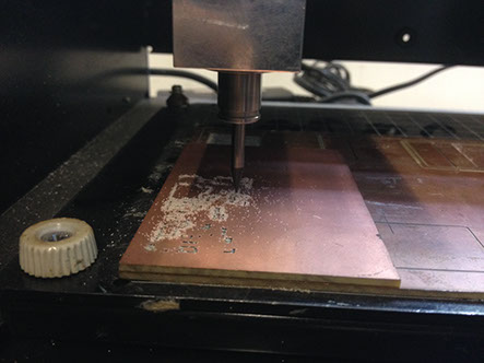
The file is loaded into the Ronald Modela milling machine hardware. The first thing that I did was to set the zero for the machine at the top left corner of the base of the machine.
The first step in to set the milling machine and start milling.
Stick the board with the double tape on the base of the board and stick it to the top most corner of the base plate.
The next step was to change the bit for the milling. I used the 1/64 inch milling bit for the first circuit milling. This includes setting the Z axis.
Once the milling starts the file shows the milling time 3.5 minutes.
The first time I made the circuit didn't worked at all. The milled board circuit wasn't good at all because the zero was not set properly during the setting of the file on the Modela.
Here is the process for the milling of the circuit.
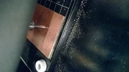
Milling the board:
The first thing that I did was to open the ubuntu loader in the fablab laptop. Once I open the ubuntu loader I clicked to the command prompt and types space_su.
Once I clicked it and opened that window and add the password twice and a new window opens up asking the file type to be loaded.
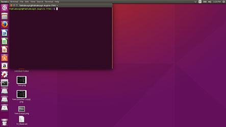
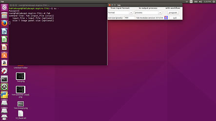

Once the tab is open I selected the file format to be .png and selected the Modela model and clicked the make_png_rml button.
And a new tab is opened which had all the details of what and how I can mill. In the window I clicked the load.png button and loaded the png file to mill. The traces of the circuit was downloaded from the Fab academy archive.

Once the file is loaded It shows up what kind of png file you have selected. Now the next step is to set the parameters of the milling of the board.
The diameter of milling, size of the drill bit(1/64) and the offset and the intensity is set and the path is made.
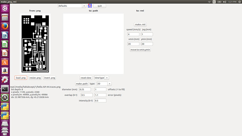
Once all the parameters are given to the file check the path and set the ZERO x and y axis of the drill bit. All the setting is done now its turn to set the z axis zero. After doing the zero setting the drill bit is taken to x min and y min and the make.rml button is pressed.

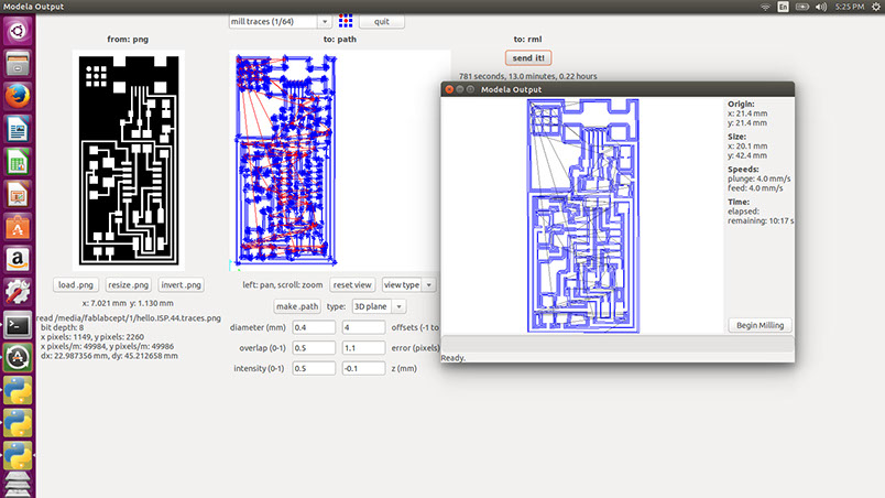
After setting the .rml now the board is ready to mill. I just pressed the send it button and milling is begin using the fixed parameters.
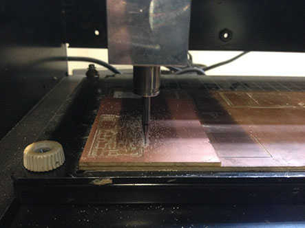
Once the traces are milled then the board is ready to get solder. But still its not completely ready for solder as the board is still not in the proper size . Now to make it hand-able the cutting file is loaded from the fab archive which isa rectangle slightly bigger then the traces.
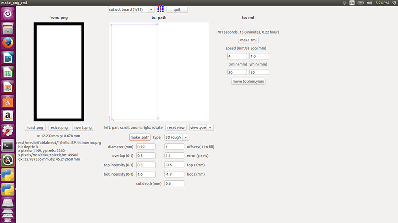
The same procedure is followed for the cutting of the board. The drill bit is changed from 1/64 to 1/32 for cutting of the board and the parameters are set for the cutting of the board.

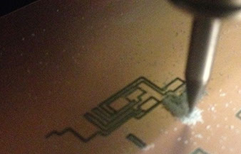
These are the milling traces of the fab Isp board. The first was the failure as the milling depth was not fixed at a proper height and the z axis zero was not set properly. There was also error in the offset parameter while setting.


NO!!! The first milling turned out to be the worst milling of my work till now. This was actually my first time that I worked on milling. I will do it again till I get a good milled board. I started again with a new blank board and did it again.

Second trial started quite well as compared to the previous one. The first pass of the traces of the circuit was looking well in the initial stage.
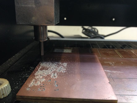
This time its going very well. I was watching each and every single move of the bit. I was very curious to see the output and in parallel I was watching the computer screen which was showing the progress.
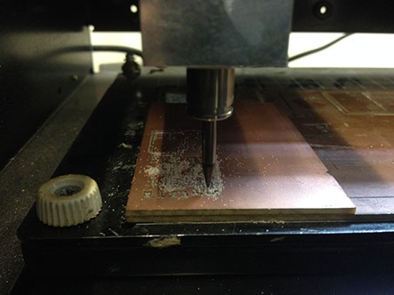


First pass is finished now its time to cut the milled board out from the unused board. Be careful not to move your board as the coordinates will change(x,y). I carefully changed the bit from 1/64 in. to 1/32 in. for cutting the board. And the cutting process has started.


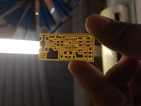
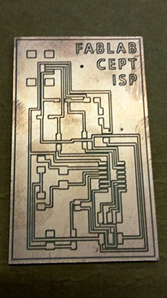
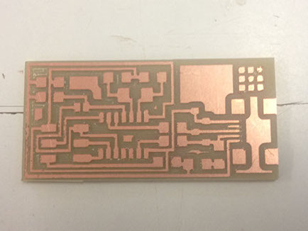
The tracks of this FabISP is broken as you can see the image so I made a new board with all the tracks fixed and now it is ready to solder all the components
Result of the changed setting for the milling of the board and
The result of the calibration was:
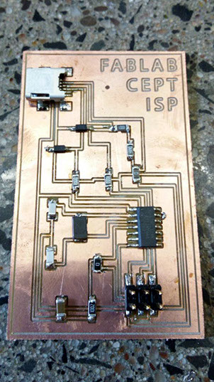
I started soldering the ISP board taking each individual components and keeping them together and soldering them one by one.
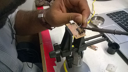
The first ISP board took at least 4 hours to complete. I was happy to see the board solder. Once the first board was complete I gave a try to see if that board works or not.
Making a SMD was my dream that I can make my own SMD and solder it.
I started it for the first time. I collected all the components required for the board and started soldering.
The biggest piece was done first and later the other pieces were soldered one by one to the circuit.
Once all the components are soldered to the circuit the chip is than cleaned for the final finishing.
All the extra solder alloy is than removed from the circuit and checked if there are any connections between two members.
Once this is done the firmware is installed from the Fab archive and the hello board is connected to the computer.
The board turned out to be over powered as there were few tracks that were over soldered and covered with the lead. Then When I CONNECTED THE BOARD TO AVR IT SHOWED RED LIGHT.


To understand how the AVR works and what lights indicate what message I checked the google weg page site.
.jpg)
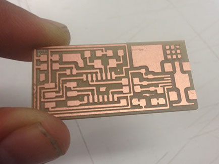
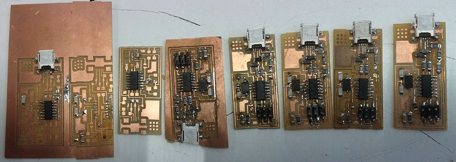
I gave many trials to solder Fab ISP board. I milled around 10 boards to learn and understand how the soldering works and also how I can get the best desired result. Here are the series of the boards that are made by me and making each one was fun.
After giving 7 trials I finally achieved my level to solder very neatly and precise and now ready to connect again with AVR and check the board.


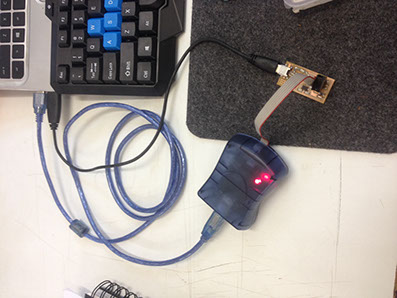
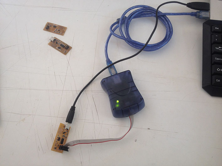
Once the circuit is complete and neat. Then the board is ready to connect to the computer. I CONNECTED THE FAB-ISP TO COMPUTER.....and...WOWWWW IT WAS DETECTED IN THE UNKNOWN DEVICES AND It passed the smoke test.
.jpg)
Now I HAVE CONNECTED THE AVR to the Fab ISP and....Bingooooo...I got a Orange blinking light fleshing in AVR. Then I removed the six pin connector from fab ISP and re-connected it properly and ...WOOWWWW iT WAS SUCCESSFULLY CONNECTED TO THE AVR and ready to program.
FAB ISP CONNECTED TO THE AVR SHOWING THE GREEN LIGHT THAT SHOWS ALL THE CONNECTIONS ARE CORRECT
FAB ISP IS SOLDERED WELL AND THERE ARE NO ISSUES WITH IT. SO Now I WILL PROGRAM THE BOARD WITH AVRISP mkll
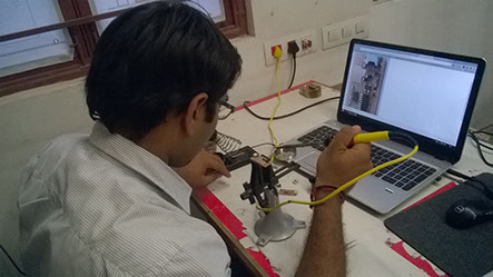
I started programming the FABISP board with the help of reference of LINK
STEP BY STEP OF PROGRAMING OF THE BOARD
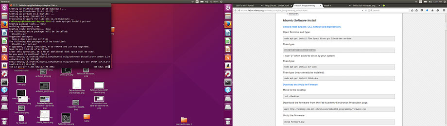
I decided to work on ubuntu for the programing of the fabisp : Software Installation for AVR
Open Terminal and type:
sudo apt-get install flex byacc bison gcc libusb-dev avrdude
Then type:
sudo apt-get install gcc-avr
- type "y" when asked to do so by your system
Then type:
sudo apt-get install avr-libc
Then type (may already be installed):
sudo apt-get install libc6-dev
Download and Unzip the Firmware:
Move to the desktop
cd ~/Desktop
Download the firmware from the Fab Academy Electronics Production page.
wget http://academy.cba.mit.edu/classes/embedded_programming/firmware.zip
Unzip the firmware
unzip firmware.zip
POWER the Board: These are the screen shots of programing :

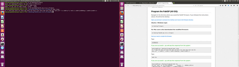

cd Desktop/firmware
Type:
make clean
Next task is to Type:
make hex
Next Type:
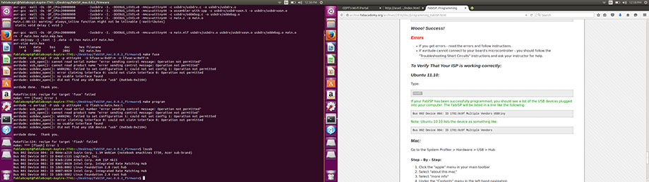
make fuse
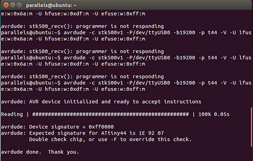
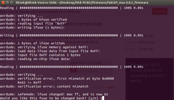
WOW I have done the programing of the board. This is the message It showed me: