Home
Biography
Projects
Final Project
Input Devices
This week I decided to read a value from a potentiometer and control the blink speed of an LED. I used a board that I plan on using in my Final Project, what I call the Tiny I2C Node.
Design
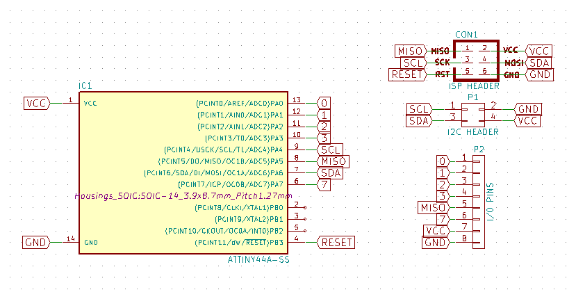
Just as I did during the Electronics Design week, I used KiCAD to design My circut board. This board was designed to communicate with a main board that would supply power over the I2C Cable, But I figured It could run standalone when powered over the SPI header.
When laying out the schematic, I first dropped all of the components I thought I would need onto the board. I tried to use as few parts as possible (no jumpers or even an external resonator). Parts include the ATTiny44, an ISP header, I2C header (2x2), and 8 pins for I/O. Then I used what KiCAD calls global labels to connect each pin on the 44 to the proper pin on one of the headers. global labels make the shematic look cleaner and allow me to add components like jumpers mid design.
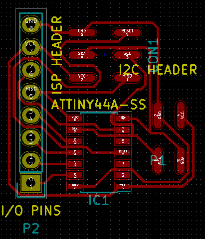
 Nothing special was done during PCB Layout, which primarily involved pulling my hair out while trying to make every wire connect to it's destination with as few jumpers as possible (I ended up needing none). I ended up widening some of the wires to allow my chemical bath (discussed later) to etch the boards with less of a chance that the traces will fall off in the bath.
Producing the boards was the interesting part of this week. I used a chemical bath of Hydrogen Peroxide, vinegar, and table salt to dissolve (ok, react) copper off of boards. To start this process, first I export the
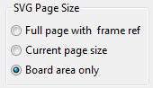
board layout to an SVG. I have learned from my mistakes from previous weeks, when I exported with the massive border around the circut. In KiCAD, you can choose to export only the circut and the area around it. This is done by clicking the "Board area only" option in the "SVG Page Size" area of the SVG export menu.
I then imported the
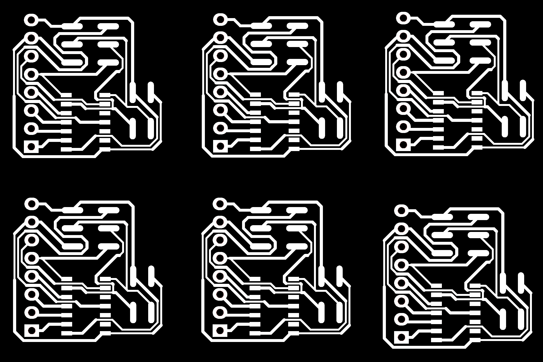
SVG into GIMP with a DPI of 750, to guaruntee that the board would look nice off of the laser cutter. I bucket painted the background of the board white, and inverted the colors. I painted all of the traces white (we want to keep those) and selected everything with Ctrl + A then copied with Ctrl + C. I created a new image in GIMP with the dimensions of the boards we have (2" high by 3" wide in my case). I pasted the board into the new image six times and arranged them so that the boards do not overlap. I then painted the background black. I tiled the boards so that as little copper as possible is wasted in the solution.
I
then exported the file to a PNG and moved the file to the laser cutter computer (alternatively, you can do all of the AI steps then move the AI file). A that computer I opened the file in Adobe Illustrator. In AI I made the image more smooth and less jagged with the image trace tool AI has. This is located in the top bar when the imported image is selected.

You can now begin burning off the etching resist with the laser cutter.
Laser Etching of the Resist
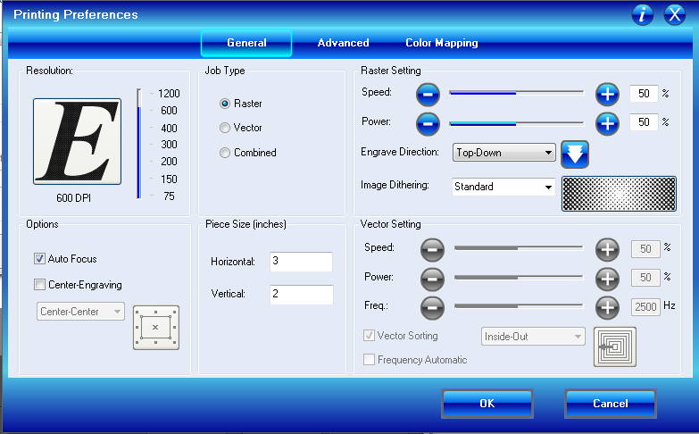
I first set up the 40W laser cutter (turn on the pump and air filter too) and opened the settings for the laser cutter. I set the cutter to raster only, turned on autofocus, and left the DPI at 600 and the power and speed both at 50%. At 50/50, the cutter takes more than run to complete the board to an etchable state, but at 100% power, the lasing is innacurate and at 25% speed the cutter takes too long.
But before you can run anything, you must have a board to etch.
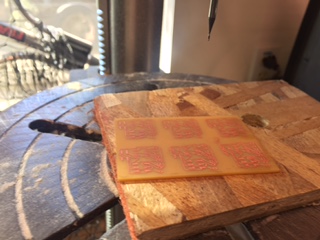
The board will be protected in the chemical bath with masking tape (I use 4" Avery masking tape), which works suprisingly well despite it being essentially paper and adhesive. To apply the masking tape, take a piece of tape a little larger than the size of your raw board, apply it, and squeegee out any air bubbles. Then flip the board over and trim excess tape from the board.
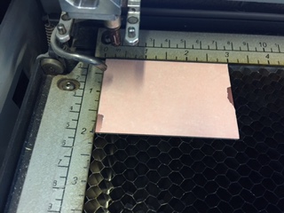
Then apply two or more strips of double-sided tape
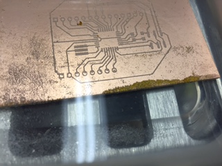
to the untaped side of the board. This will prevent the board from moving during the autofocus probing of the second run, which could ruin thin traces. The board can now be placed inside the laser cutter near the zero of the machine (like in the photo above).
Now run the job you sent to the laser cutter
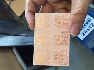
earlier (or send it now if you didn't). The job, depending on your laser cutter and the size of your board, can take 2 to 6 minutes each run. Wait for the job to finish (stay around, you're essentially burning paper off of the board) and repeat the job when the first run is finished. When you are done with the second run, there should only be a thin layer of adhesive left on the board. (The image below had the colors revesed by accident before cutting)
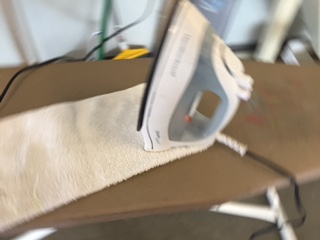
Now take the board to a clothes iron. Turn the iron on and place a cloth over the board. Once the iron has heated up, apply the iron to the board and press and rub firmly on the board. I did not use steam. Once that is done, remove the cloth (the cloth may stick, pull it off gently) from the board. I ironed the board because I felt that ironing it would help the adhesive stay adhered better in the chemical bath. So far this has remained true.
The board is now ready to be etched in the solution.
The Etching Solution and Etching
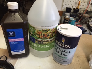
The ething solution is easy to produce and is safe to store and use. The solution consists of vinegar (any acid can be used, but vinegar is safer), hydrogen peroxide, and table salt (only needed if you are using a weak acid like vinegar). The solution (as I make it) is therefore safe enough that you could essentially drink it (please don't). These ingredients can be bought at any grocery store, and the more concentrated and pure the better (see note below on the salt) All ingredients but the salt are in a 1:1 volumetric ratio.
Note on the salt: try to buy salt that does not contain any anti-clumping agents, because they act as bases and react with the vinegar, reducing the concentration of the vinegar (and thus the rate of reaction). If you can't find any of these, be sure to add only a little salt.
Mix enough of the
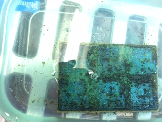
ingredients together so that the total solution is enough to substantially cover the board. You can hardly tell the difference between the solution and the ingredients in terms of color, so if you are storing the solution (I don't reccomend this, the peroxide will decay over time), be sure to label the container. Now mix in the salt and submerge the board. If enough salt is used, you will be able to see a thin yellow-green film forming on exposed copper, like the one below on my output devices board.
Now wait from 30 minutes (This is what I heard was the wait time on the internet when photo resist is used) to 12 hours (the longest I have waited) for the board to finish. The wait time is determined by the ammount of salt and the concentrations of the ingredients used. Avoid brushing or rubbing the board as some websites suggest for other resist methods, as traces become very easy to lift once the board has sat in solution for some time.
One the board is done etching, remove the board and rinse any of the solution that is left off. While rinsing, you can rub the masking tape off the board, exposing the copper. To dispose of the used solution, dilute the solution and then dump a little. repeat this process untill all of the spent solution is gone. Optionally, you could precipitate the copper back out of solution with some aluminum foil, making it easier and safer to dispose of. I reccomend using the container for etching alone from this point forward, as dissolved copper compunds are pretty much toxic in some form to all forms of life (which is why I dilute heavily). Cut the boards apart with your tool of choice and then you can solder your components to the newly etched board.
Attaching Components
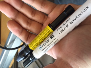
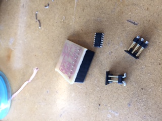
Since there may be residue left from etching, first take light, fine sandpaper and lightly sand residue off the traces. I also reccomend using a fiberglass pen for even finer sanding and a flux pen when you solder to further allow for solder adhesion. While using the fiberglass pen, I strongly reccomend avoiding toughing the tip of the pen, and if you do, wash your hands before doing anythinging else. These pens want to make you itch.
If your board includes through-hole components, like mine did, You will need to drill holes in the board. I used a 1mm drill bit (1/32" in the photo, it was earlier) and a drill press
to accomplish this. If you did not leave the holes in the lasering png, you will have a much harder time creating the straight line of holes neccessary for through-hole headers to be attached.
You can now solder your components to the board. I strongly reccomend having all of your components in one place and sorted; and a copy of your board layout and schematic nearby.
Apply solder flux to the pads and solder low-lying and temperature resilient components first, to avoid damaging microcontrollers. Then solder the inner through-hole components. Then solder the microcontrollers and then taller, larger components and outer through-hole components.
Your board is now complete and ready for programming
Programming
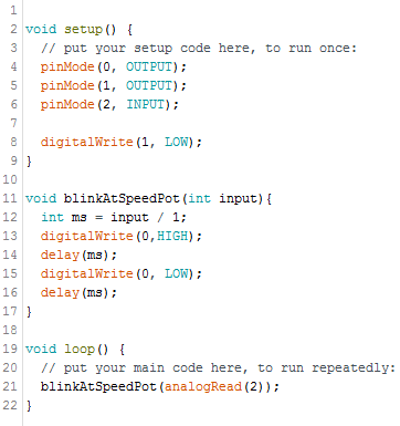
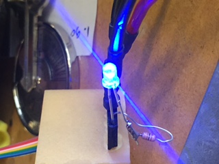
I wrote a simple program that will vary the blink speed of an LED based on the value of a potentiometer. The program reads the value of a potentiometer from an ADC pin and calulates the blink delay of the LED from that value. The program the uses that delay to blink the LED, 50% on, 50% off. Since ADC pins read voltage, I wired one outer pin of the pot to ground, the other outer pin to VCC, and the center pin to the ADC pin.
ADC pins will be able to read analog inputs, but not write them. There is a dedicated function for reading these and there is no reason to set them to an input (even though I did). If you wish to use digital inputs, simply declaring digital pins will do.
ADC pins
can be found in the datasheet, along with pin numbers in the IDE (It's P_# where # is the IDE pin number and _ is some letter, at least for the tinies).
To program, I set up the IDE to program the chip for 8 mhz internal for the tiny 44 (requires the
support pack (not what it is called, but oh well) found here). I then plugged the FabISP into the computer, the wires to the board the right way around and verified and uploaded the program. If the IDE continually spits out verification errors try different USB ports and restarting the computer. If an r=-1 error appears, try probing around with a multimeter for high-impedence connections and resolder them.
If somewhere in the programming process your chip starts to smoke, disconnect the ISP immediately and redisign your circut or resolder with a new chip in a different orientation, since the positive and negative connections may have been reversed.
You now have a working chipset with a working input.
Files:
LEDBlink.ino - program shown above
TinyI2CNode.zip - unpack and open in KiCAD
Board image (PNG) - resized to avoid dominating the entire screen.