Home
Biography
Projects
Final Project
Electronics Design
Choosing CAD
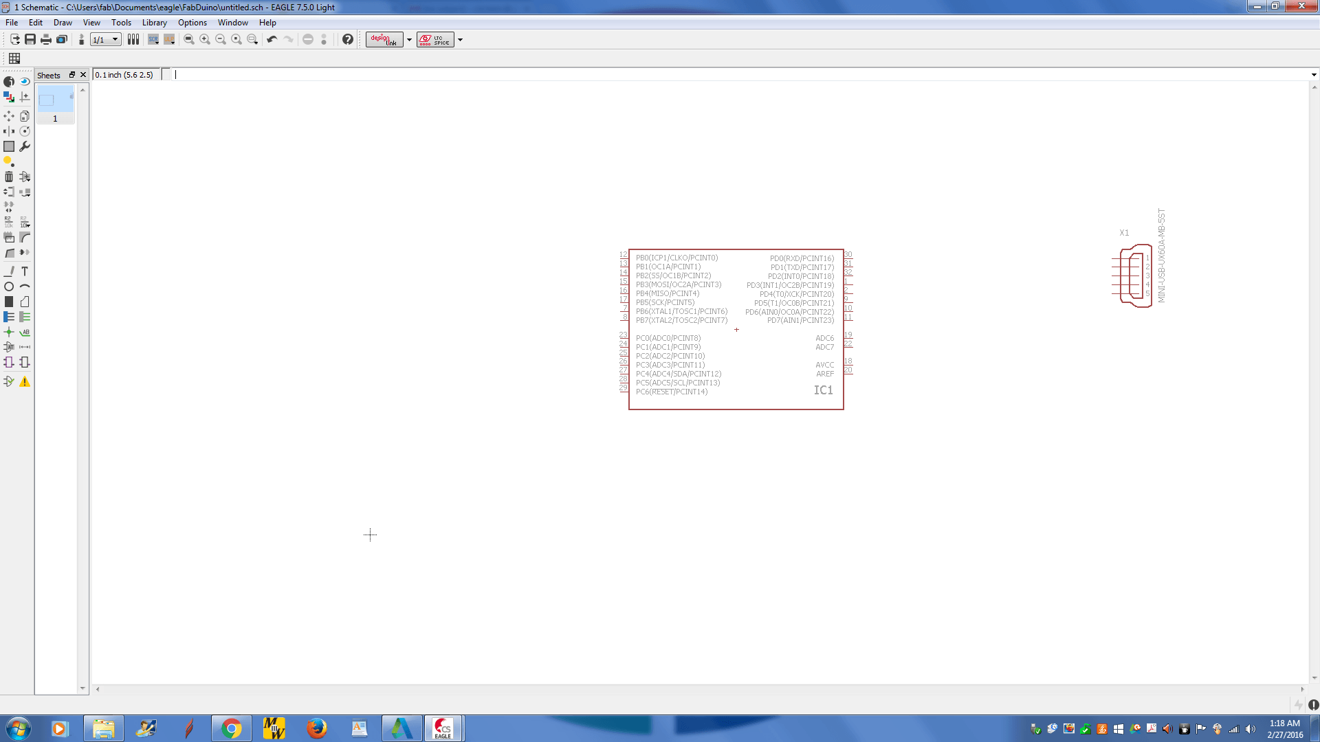
I first tried making a potential final project in Eagle. I have had plenty of experience using Eagle, as our FabLab has used the free version for a long time. I liked the auto-router program that allowed me to quicly get my board wire. Most of what I have done has involved creating simple boards with only passive components, however Eagle seems to lack the components necessary for the final project, namely an atmega 1284P and 32u4. Making boards that are ready for the mill has always required some work in gimp to get the black and white images you need.The free version of Eagle also places size restrictions on the board, which could be a problem for some projects.
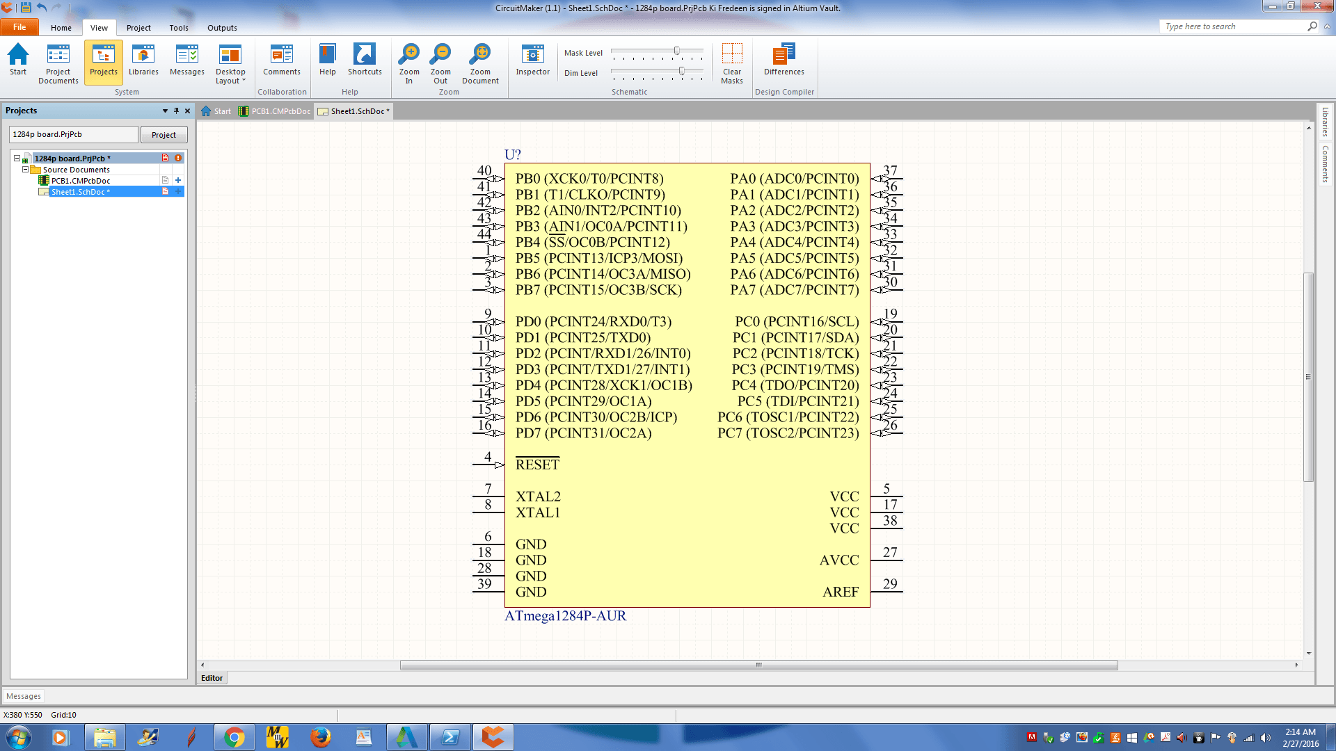
I then turned to CircutMaker, a community driven CAD program. There are some parts that come with the CAD program, but
most of the parts you will need come from the community. I found that the program's method of inserting parts into a schematic confusing (I never got past the one part shown below), and that it relied on a steady connection to the server to pull the list of parts you added to your project.
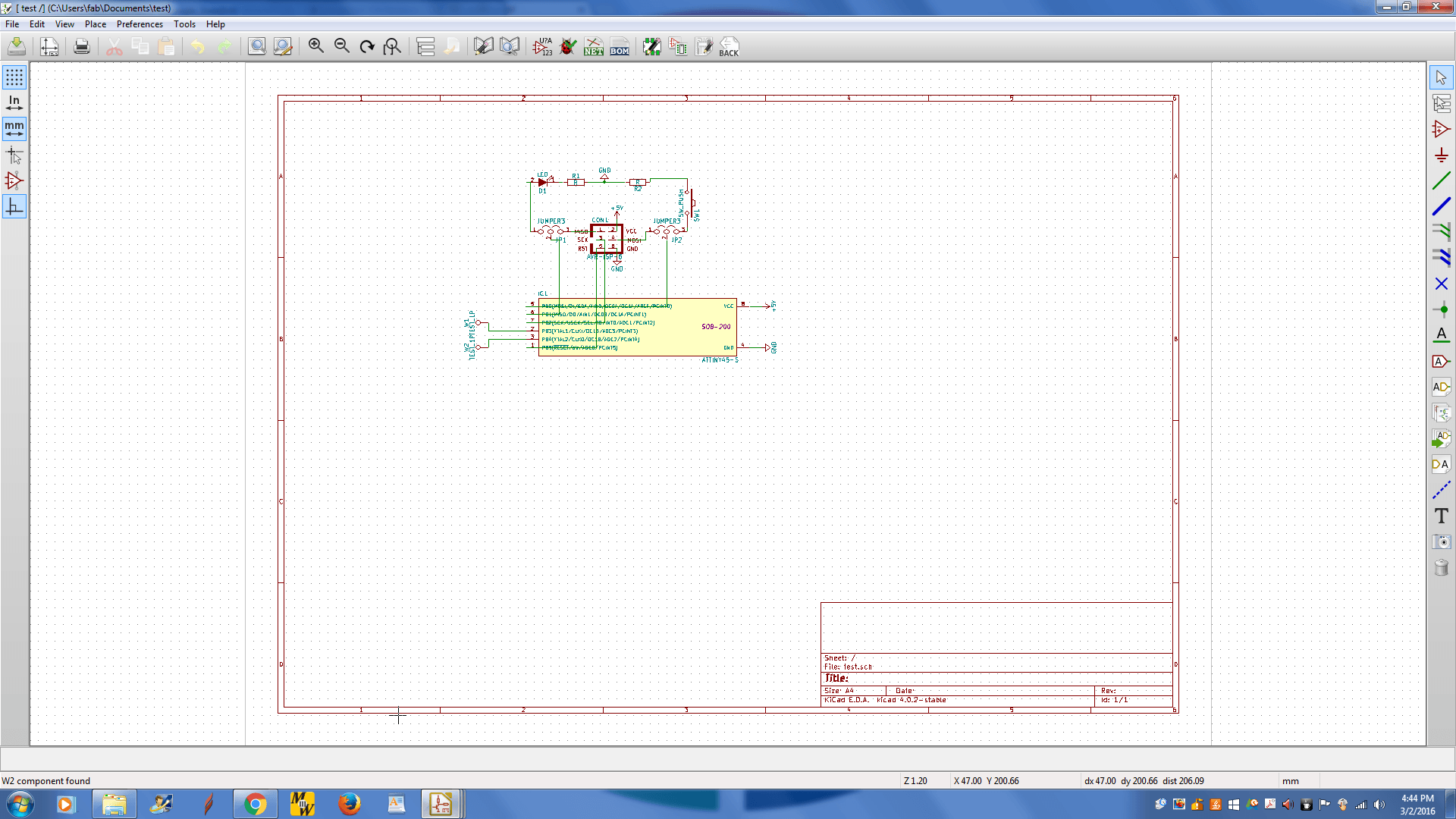
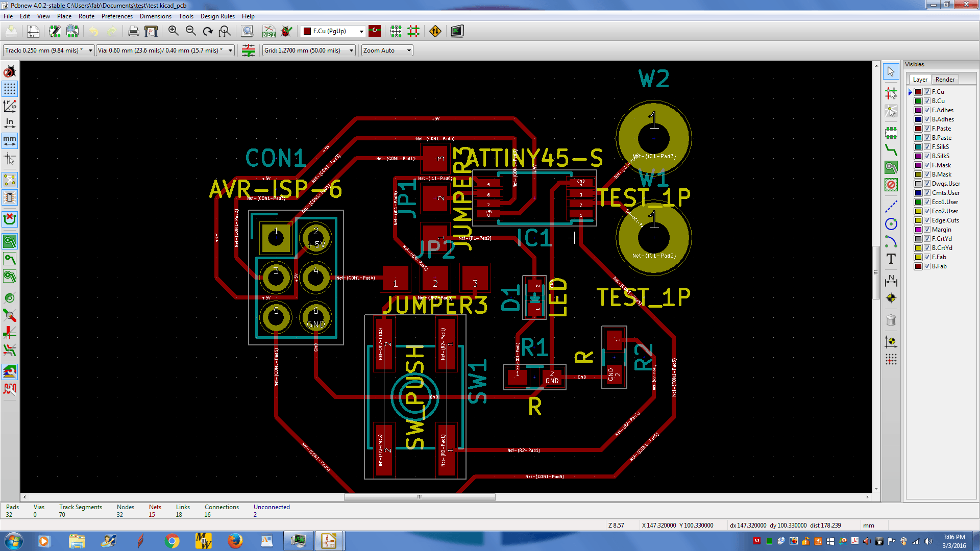
I finally desided to use KiCAD, an open source Electronics CAD Program. It had all the components I would need from the start. It has a method for adding parts to a schematic similar to Eagle.
I was able to quickly design this week's project. In KiCAD, you must select the footprint of your components before you can send them to the board layout program. This can create problems when you can't find (or are unfamiliar with) the required footprint, but this is easily rectified with KiCAD's footprint creator. It takes a little math and a pair of calipers, but it is possible to create any chip footprint avalible.
Design
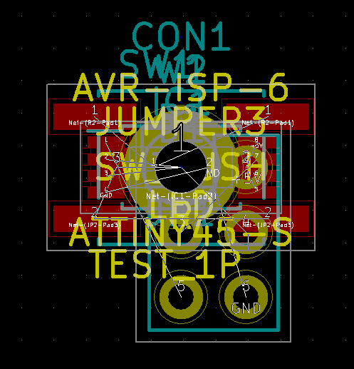
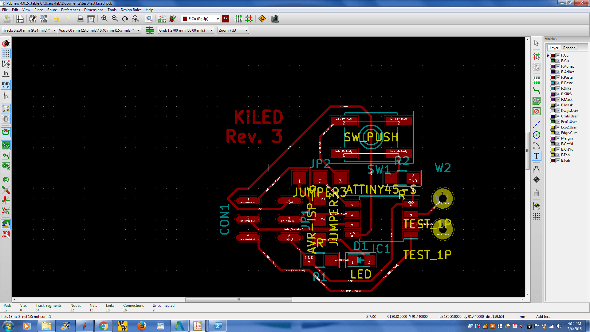
In KiCAD, I first chose the types of components I would need for this week's project. I chose the attiny 45, Because our FabLab had plenty, and that I thought an attiny 44 was too large for this project. I then linked the parts together, having jumpers leading to the ISP header, which allows me to switch between programming and use. The ISP header will supply power to the board. You can see the design above.
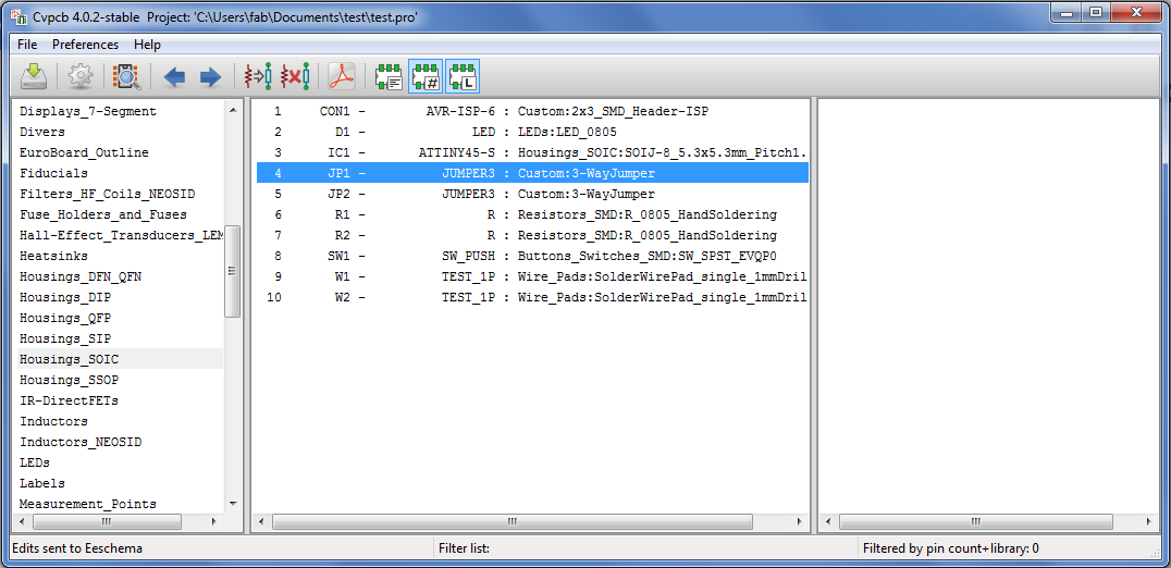
The hard part was associating components with thir respective footprints.
First you must annotate the schematic. This gives all the parts names. Then you can open up CvPcb to assign footprints to each of the components. This must be done or parts will not appear when you convert the schematic to a board. If you can't tell what the pootprint of a component is, try looking up a datasheet or measuring the components and comparing the measurements to footprints, which can be viewed with the "view selected footprint" button.
Convert the Schematic to a board with the
Pcbnew Button

KiCAD will open up a board editor. Your
components will be in a jumbled pile in the middle.
To move them to more coherent locations, right click on the pile, and when the editor asks you to clarify your selection, select a part and press M to move it. Repeat ntil the components are in the desired locations. You can now connect the pads together with traces. This is a bit of a puzzle and varies from person to person, so I won't go into it here, but a good few rules of thumb are to avoid traces coming too close to each other or to pads, make sure your mill can handle the trace width, and make the part spacing sane enough for you to solder.
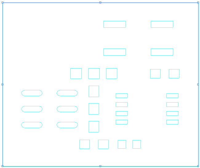
That was my first design. Notice the size if the IC pds, the two holes, and the fact that the ISP header is through hole. Below you can see the size issues with the first and second designs (The second one is sideways, but just because it wants to).
After choosing (and creating) the right footprints, my design looked like this:
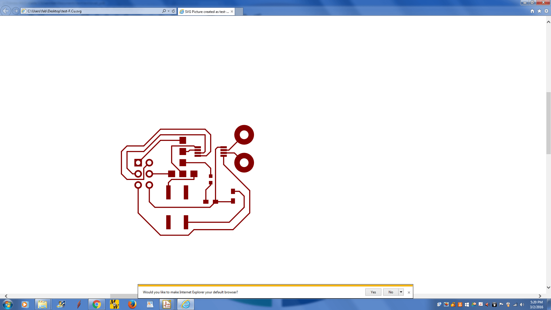
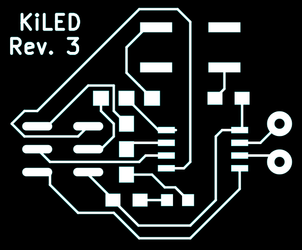
You can export the board to an SVG in the file menu. It will ask you to choose the layers exported, but you only need two right now: F_Cu (or something) and the paste layer. We will use the paste layer later to create a solder mask. The board will be surrounded with a border, so import the file into gimp (I prefer a DPI of 500 for this) and cut the board into another image of the same size.
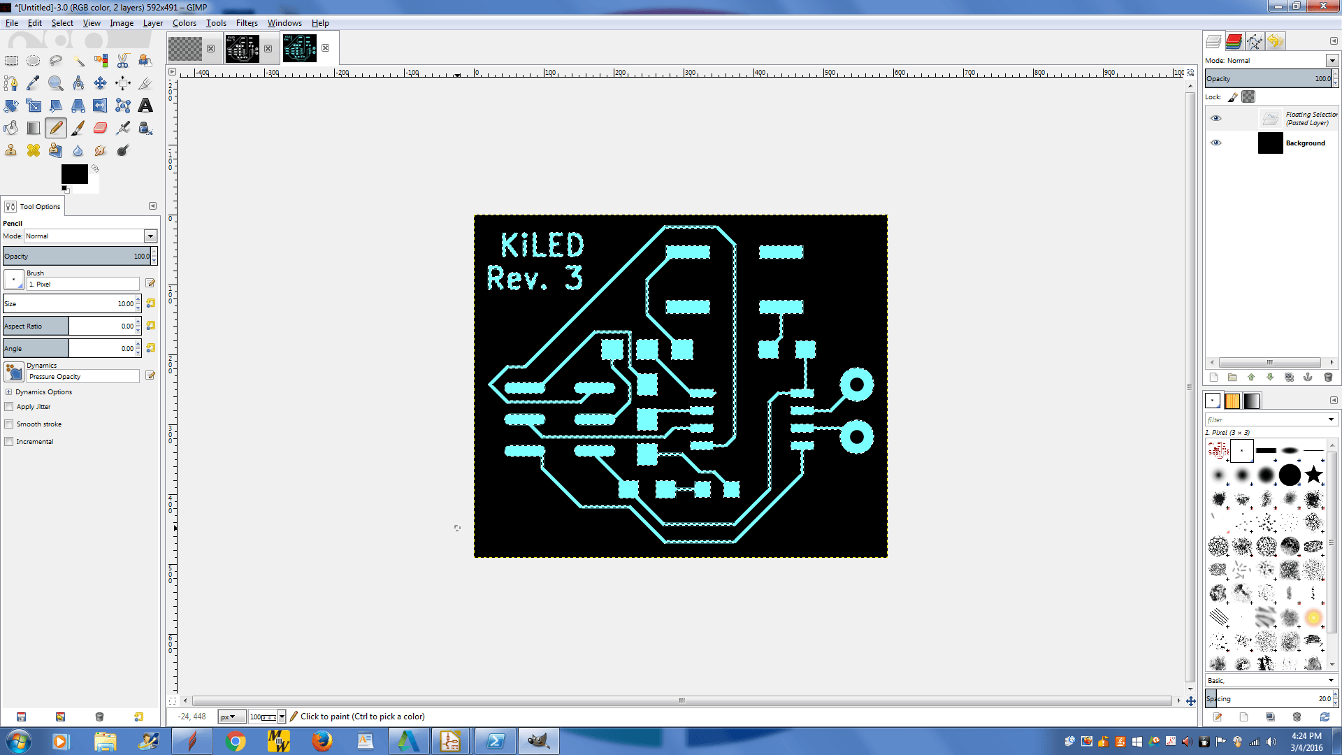
Once the file is in Gimp,
invert the colors and fill the traces with white. Make sure the background is black. At this point you can add some text to your board, but it may not turn out very well on the mill.
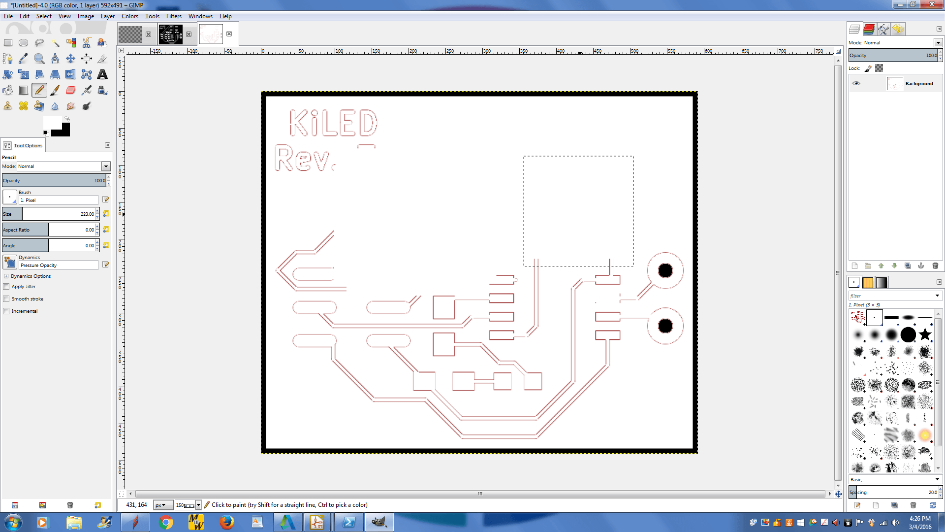
Creating the drill file
is a similar process, just leave the background as white and make the parts you want to drill out black. You will also want a black border around the board, but if you forget to do this, you can always use the scroll saw to finish your board.
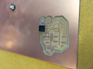
You may also need to clean up the board, as leftovers like the ones shown below will show up.
This time
I made my own solder mask with the vinyl cutter. You need to edit the SVG in a similar fashion to the traces. Then, at the vinyl cutter, you import the PNG into Adobe Illustrator, and navigate to Object>Image Trace>Make and select from the dropdown (at the top) and find "outlines." It should look something like this:
You can now set up your vinyl cutter and cut the piece and apply it to your board. Paste the solder as you would normally.
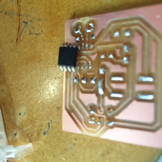
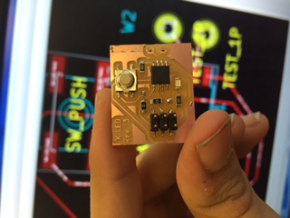
Soldering should proceed in the same manner as detailed on
the electronics production page. This is the picture of the final product (which is also sideways, to create a dramatic effect):
Files:
test - The project files for KiCAD
3-WayJumper - My custom 3-Way jumper footprint
2x3_SMD_Header-ISP
- My good-enough SMD ISP Header footprint
The traces:
The drills:

The paste: