Electronics Design
Board Design
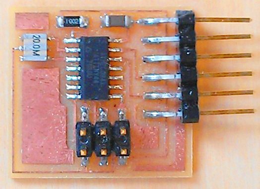
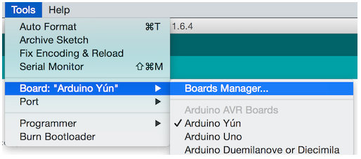
I designed the assigned board in accordance to the boards shown in the pictures below.
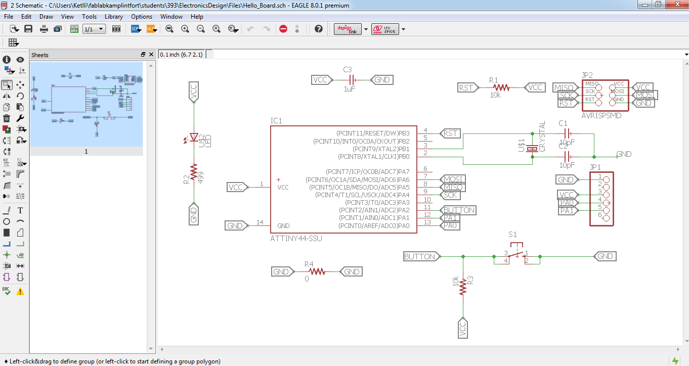
So, for this assignment I used Eagle. When I opened eagle, I went to file and choose new schematic. In order for me to be able to get started with my design, the first step was to download the fab.lbr from the archive of the Fab Academy. After that, I added the library on eagle by going to the right menu of it, press add (add is also used for adding components in order to do the schematic), choose to open a library and then adding it up.
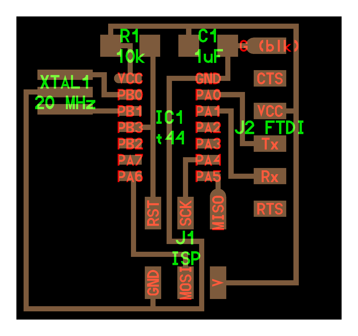
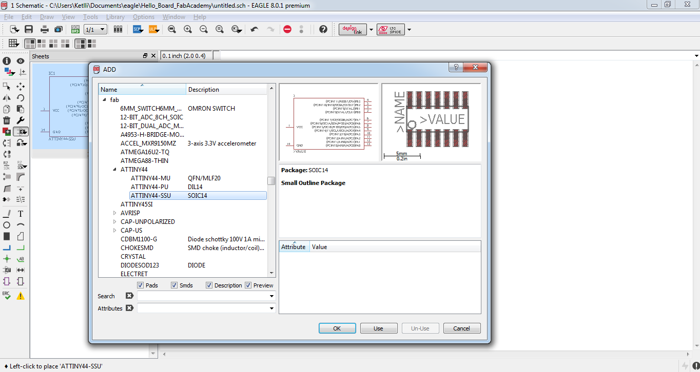
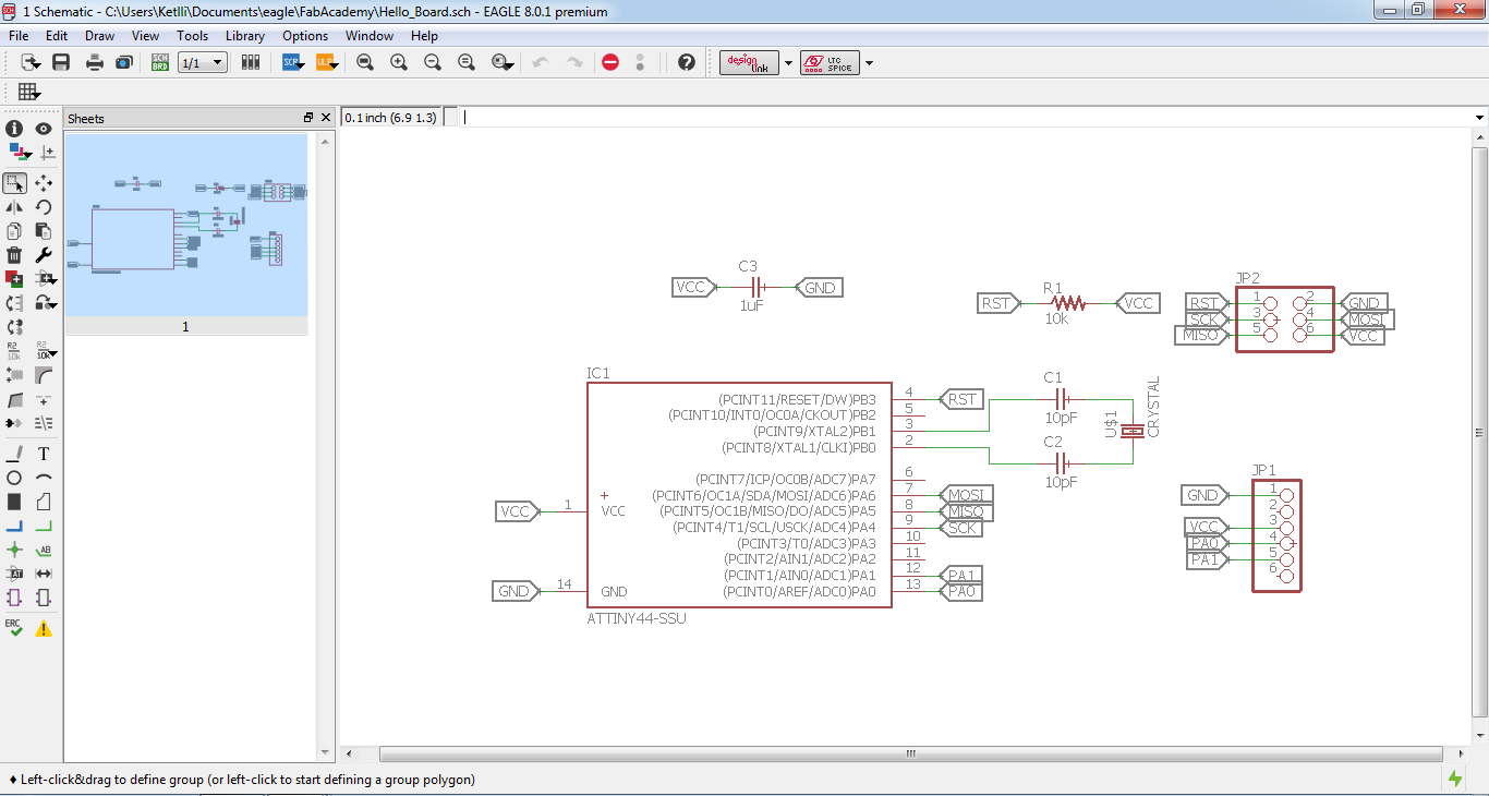
So, after the library was ready to use, I had to add the different components to be used for me to make the schematic. To add components, I pressed again the add button on the left side menu and found the different parts such as the resistors, capacitors, the crystal, the pin headers, the microcontroller and so on. In order to add values to the components added I make a right click on the component and choose the value. There is a net option to draw lines between the pads and whatever you want to connect. In order to add names in the end of those lines I used the label. When two or more lines are named after the same label, the program will ask us if we want to connect them. In my case, that was always wanted so I was pressing yes. In my initial schematic I did a mistake by putting the capacitors of the crystal before the crystal but I had to do it after. I realised this mistake only after soldering the board after my instructor pointing out to me. Also, I added a 0 Ohm resistor in order to bridge a part of my board so that I connect the grounds.
So, after putting all the needed components I had to modify the board by adding an LED and a button. For the addition of the LED, I had to read the datasheet of the led. I found the forward current and voltage of the led in the specifications and then I calculated the value of the resistor I had to use.
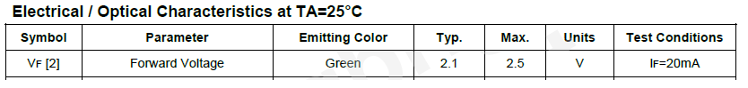
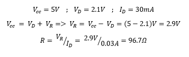
After I found a value of 96.7 Ohm, I decided to use a resistor of 499Ohm, the closest value to the one I found in my calculations. So, I went back to schematic and added the parts mentioned.
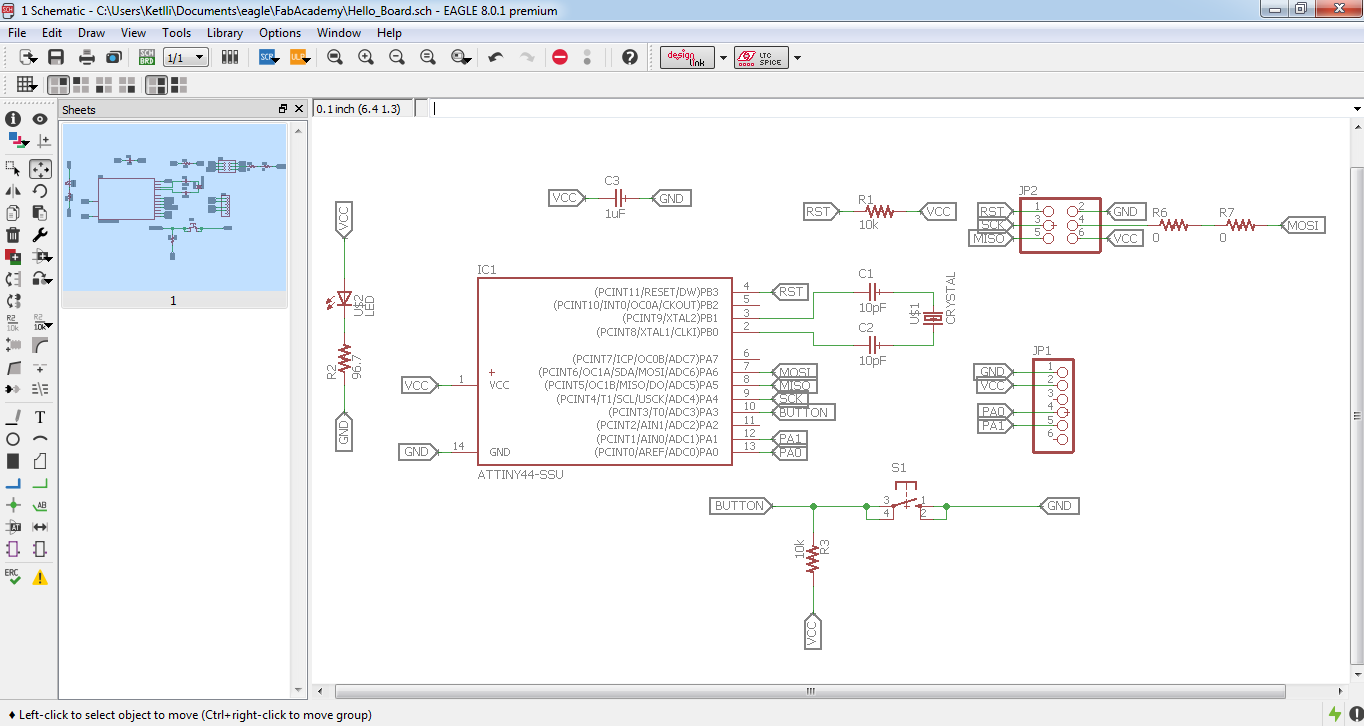
As I mentioned before, I made a mistake with the crystal and also added a 0 Ohm resistor. The schematics below though are shown with the mistake of the crystal.
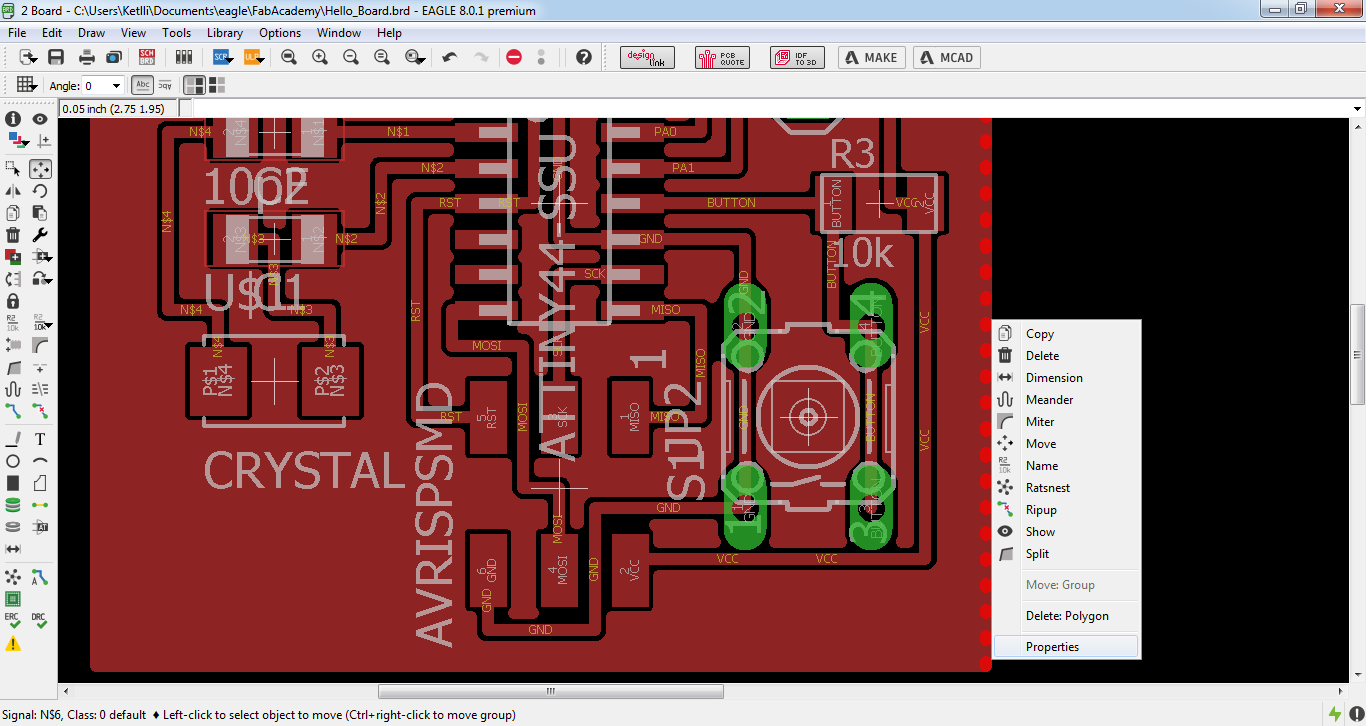
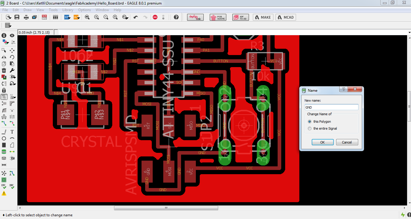
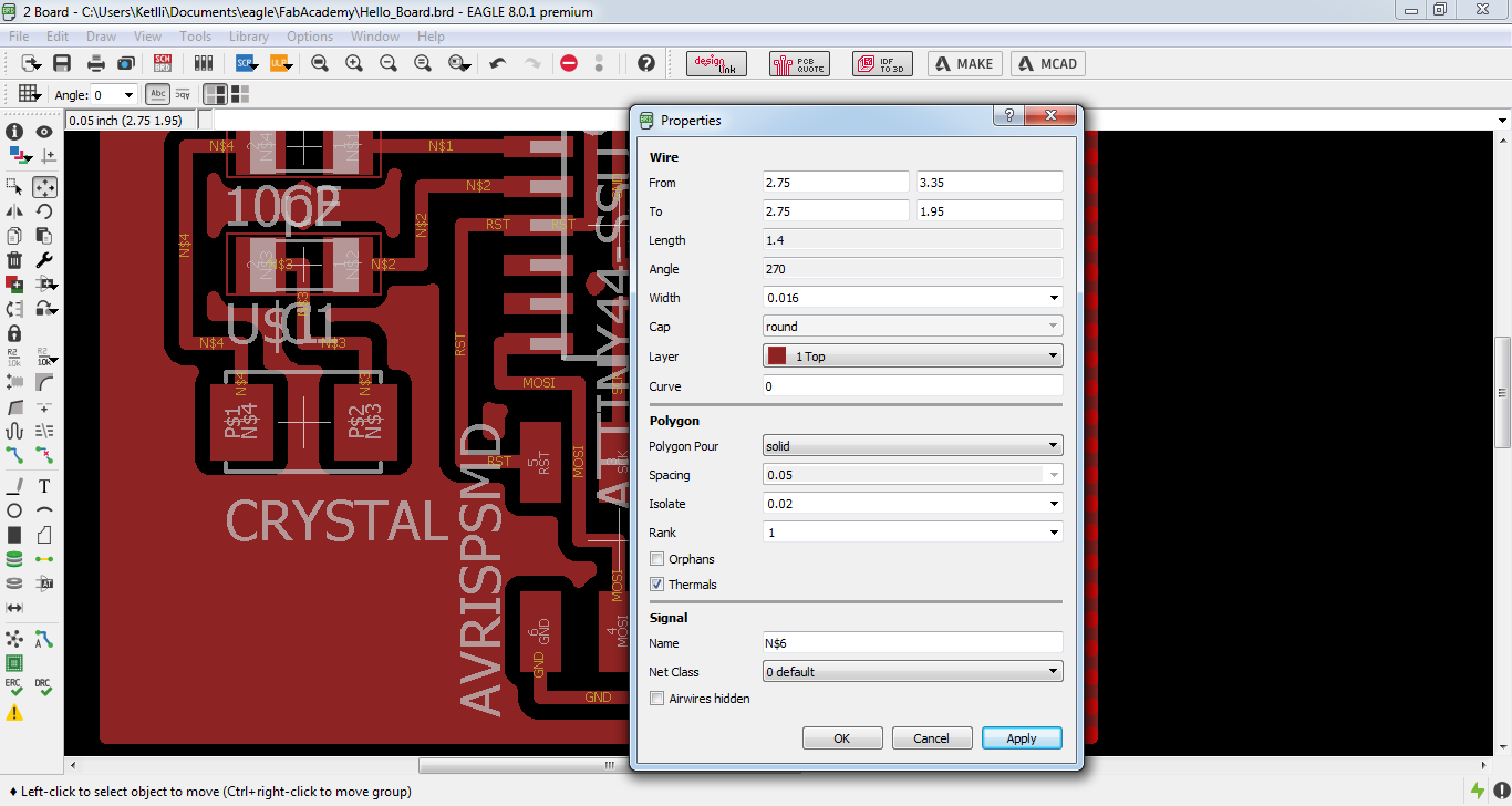
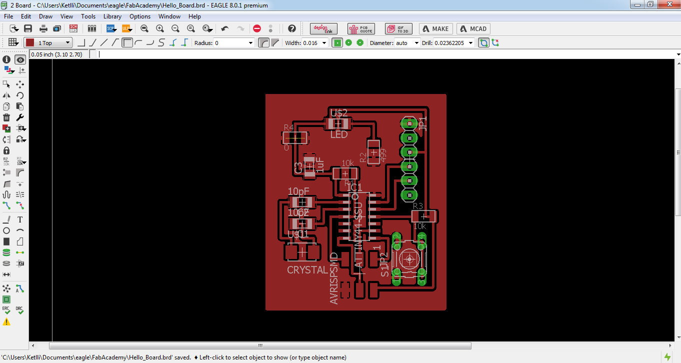
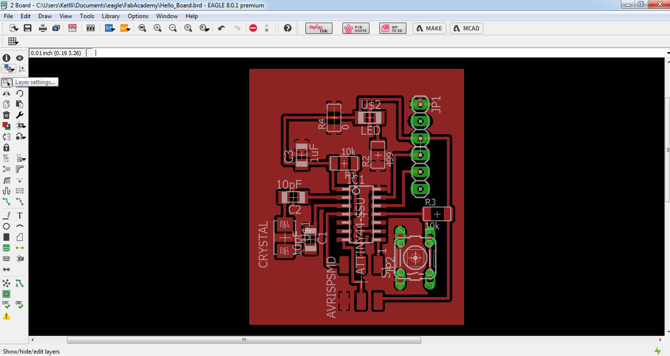
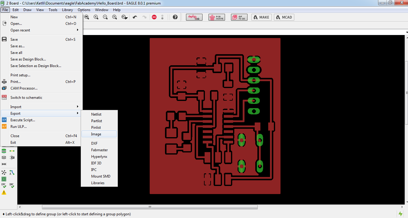
When the schematic is ready, it was time to make the board so that afterwards we can make the PBC. To generate the board, we press a small icon on the top menu of eagle that says switch to board. The first step when you go in the schematic is to place all the components in the white square. After putting everything in the square and trying to align it properly, I use the route in order to connect everything keeping into account that it will not overlap. After connecting everything what I did to lessen the connections was to draw a polygon around my design and apply rastnest to it.
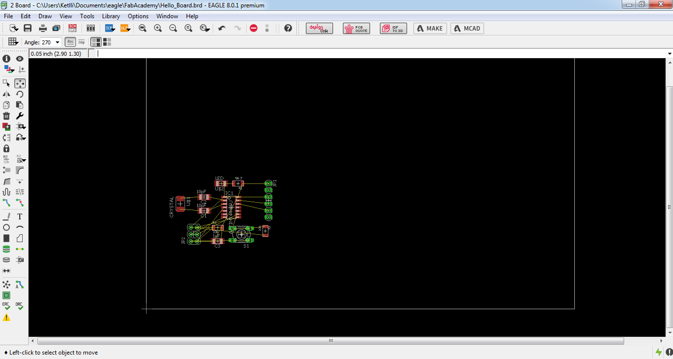
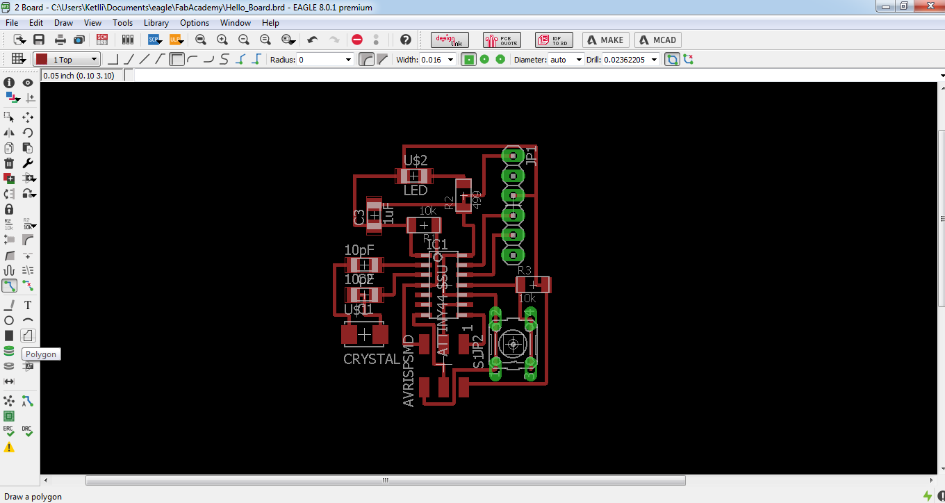
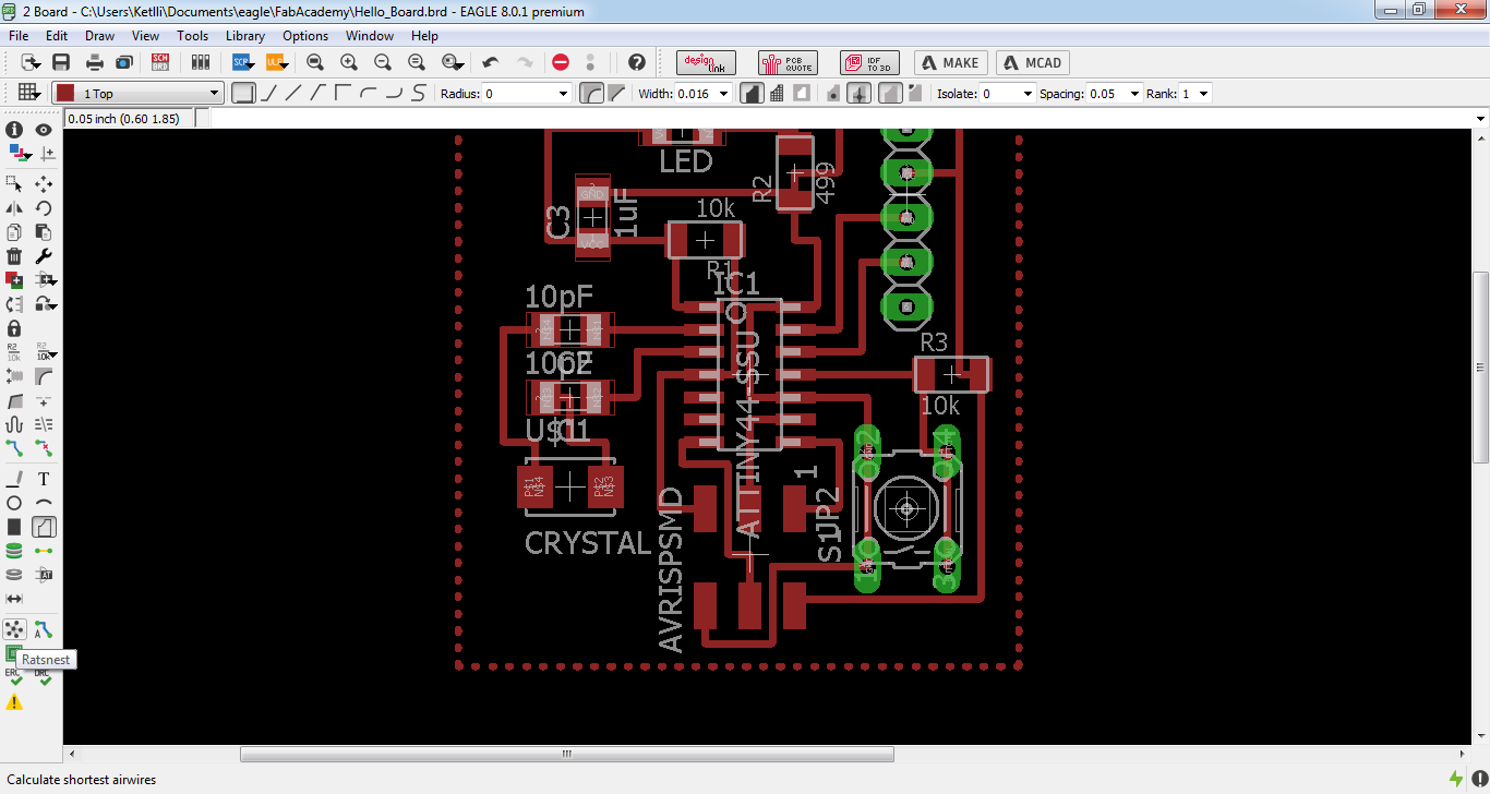
I applied rastness so that I set a value to the whole area of the board in order to lessen the connections. Apart from the value that I set to the whole board, I also set the isolation of the paths (or better described the thickness of the paths) in relation with the area of the board. To set the value of the area I right click on the edge of the polygon and choose name. For the path I follow the same procedure but instead of name I choose properties. After that my board was ready to be exported.
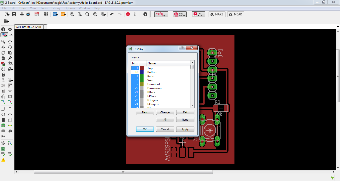
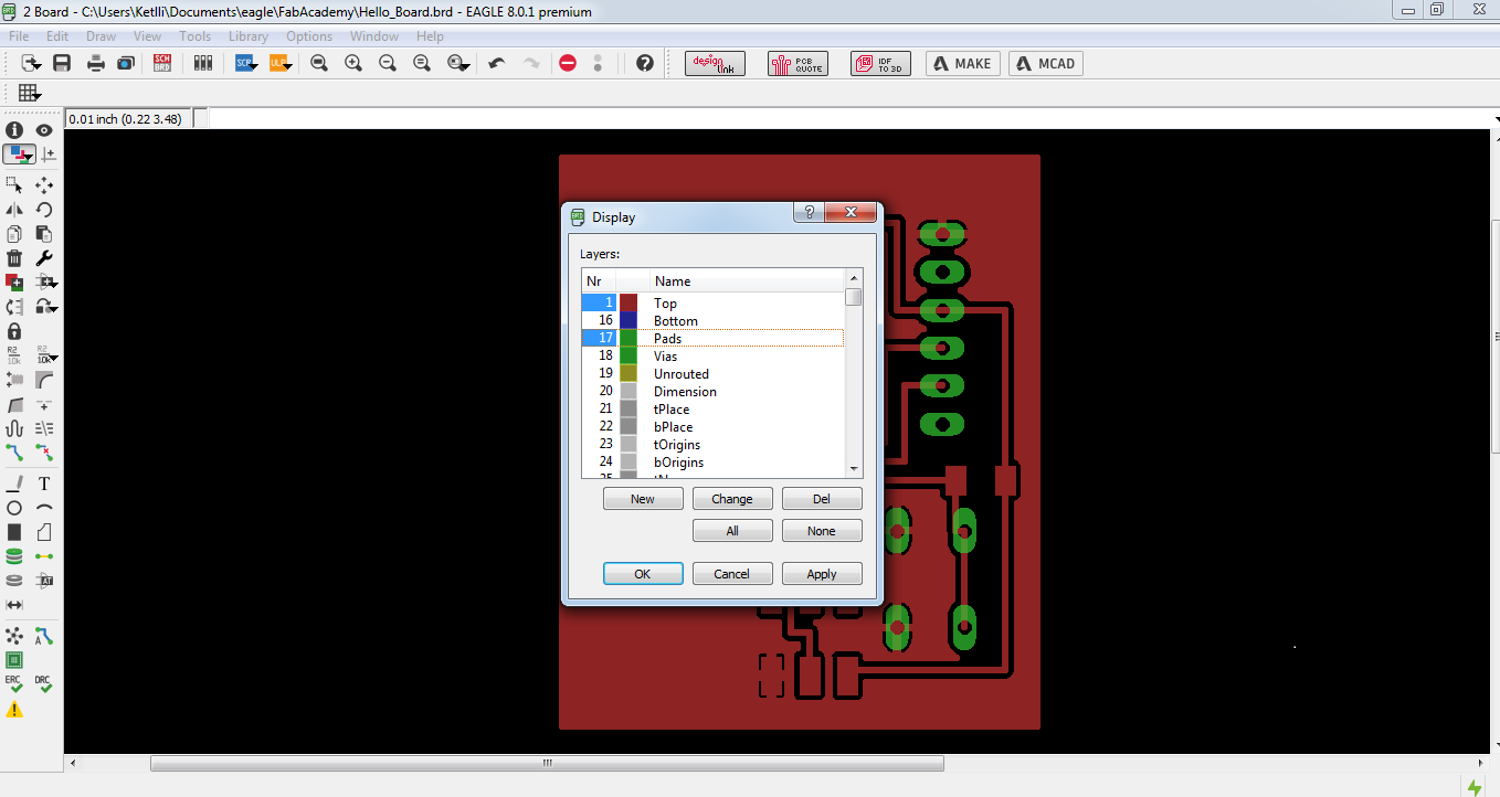
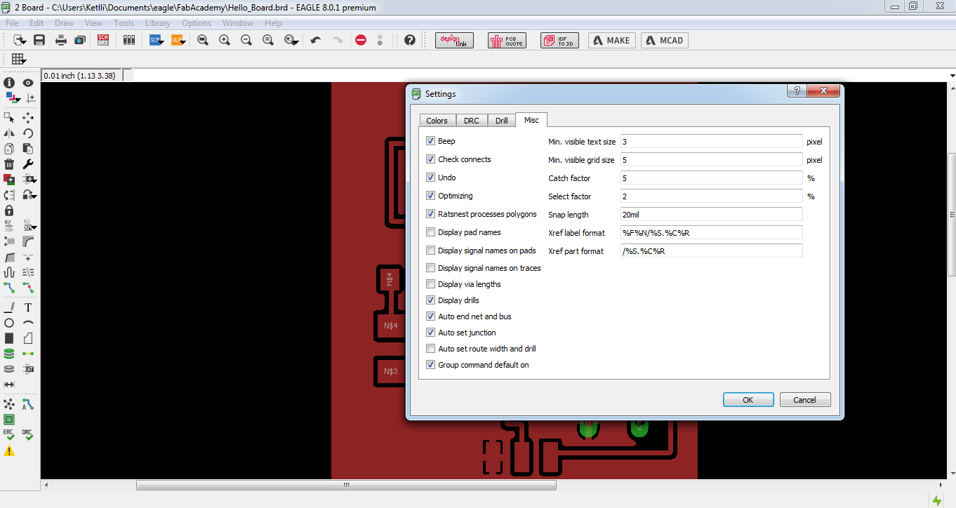
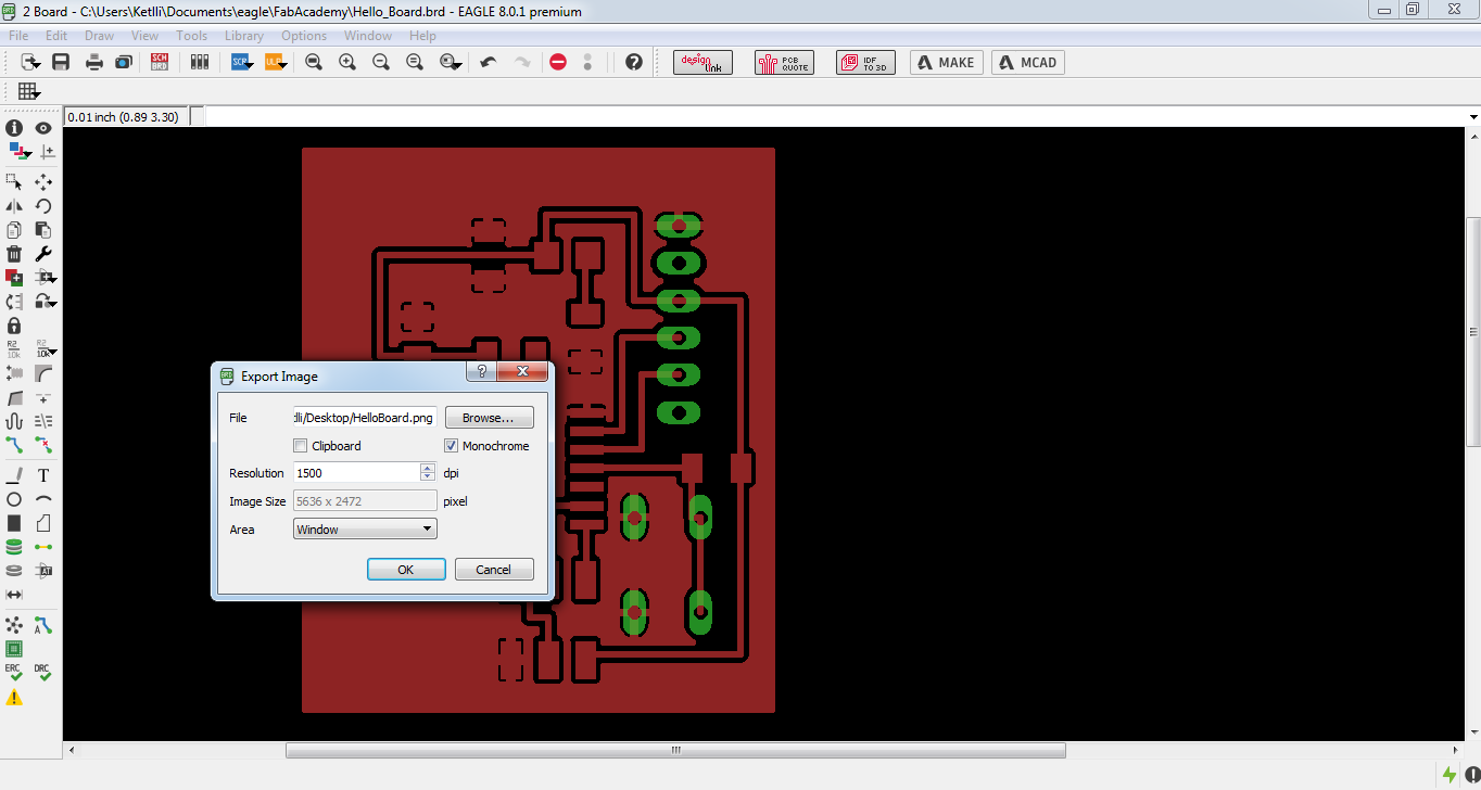
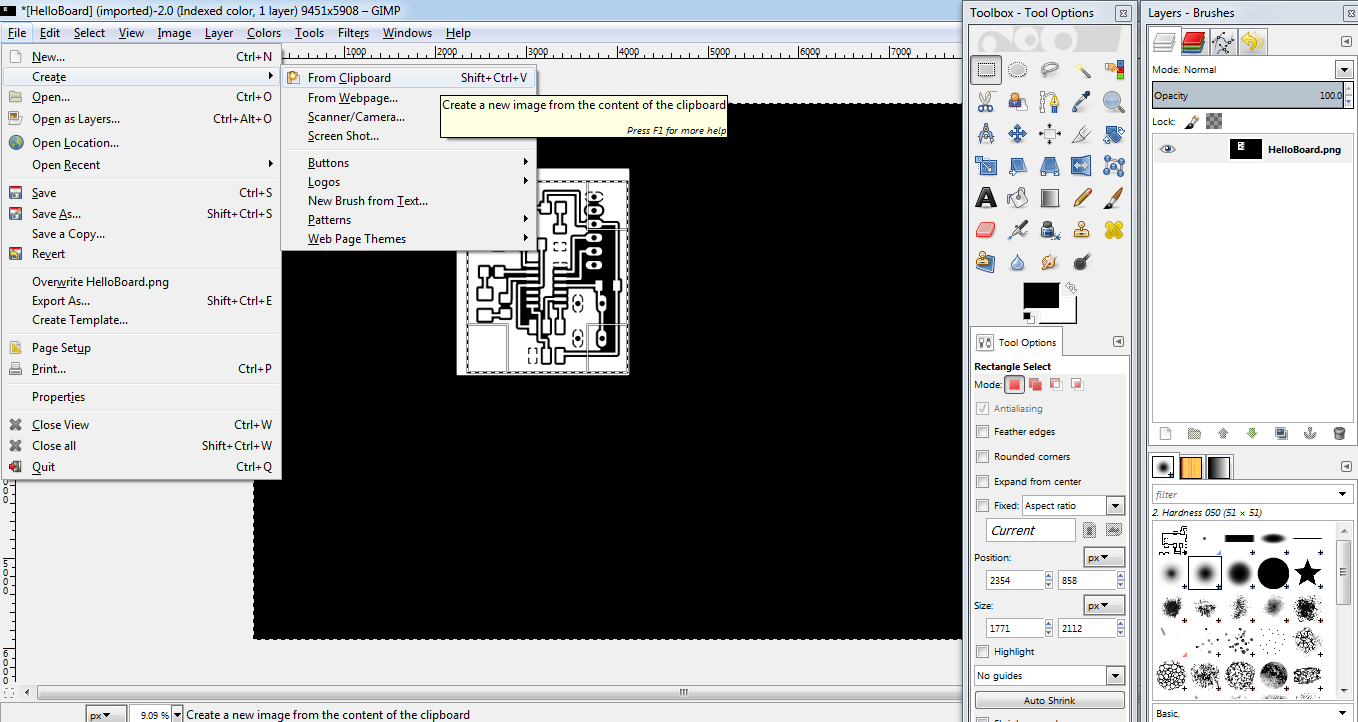
In order to start the milling process of the PCB board, I have to export an image of my board and edit it with GIMP. To do that, first of I had to get rid of all the writings. I did that by going to the layer settings, deselecting everything and then selected just the pads and the top and pressed ok. Even after that though there will still be some writings. To get rid off these writings I went to options>set>misc and I disabled couple of things.
When I was able to get rid of all the letters and have just the traces and the pads, I exported the image to a desired directory choosing the monochrome option and putting the resolution of the image to 1500dpi.
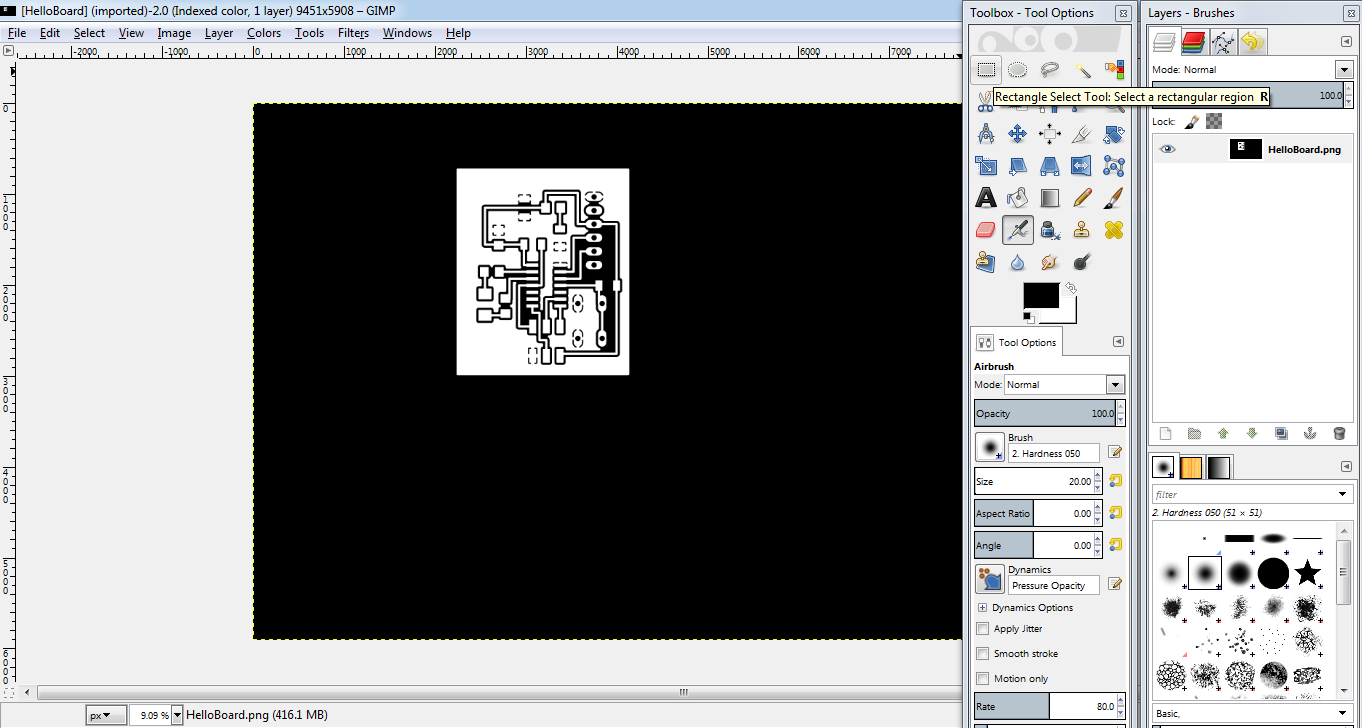
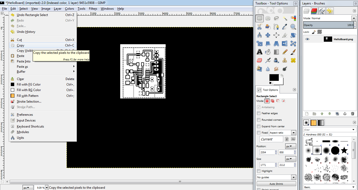
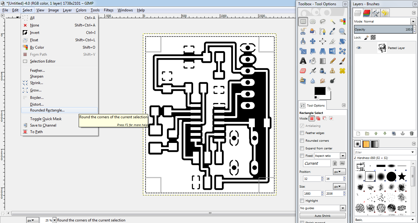
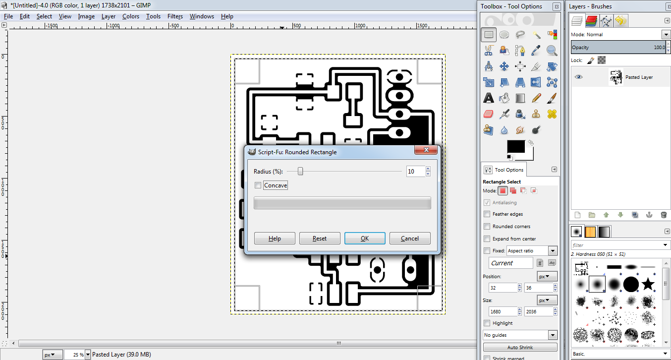
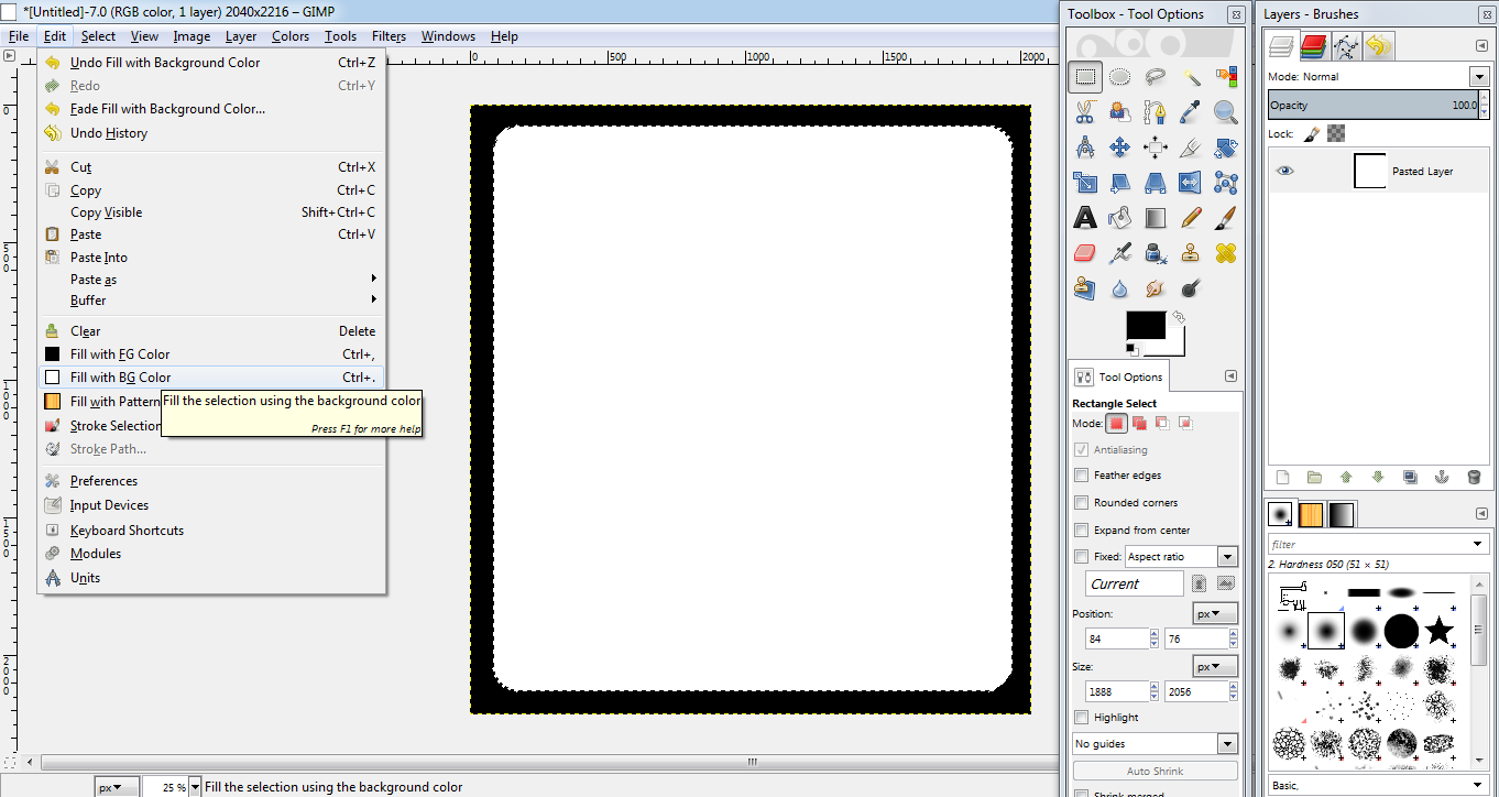
After exporting the image to my desired directory, I close eagle and open my exported picture on GIMP. I selected the rectangle on Gimp and then selecting the area I wanted to mill with it. After that I copy and pasted it to the clipboard. The first image that popped up is the internal path of my PCB. After exporting the image on GIMP as a .png then I proceeded to make the image for the outside cut. After I fill all the area of the rectangle with black colour I chose the rectangle again and rounded its corners by 10% being careful not to choose concave. Then I filled the rectangle in with white colour. The Rolland mill would not recognise it the other way around. After doing that, I have my outside cut ready and I exported that as a .png file.
Milling and Soldering
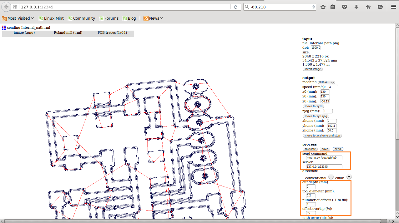
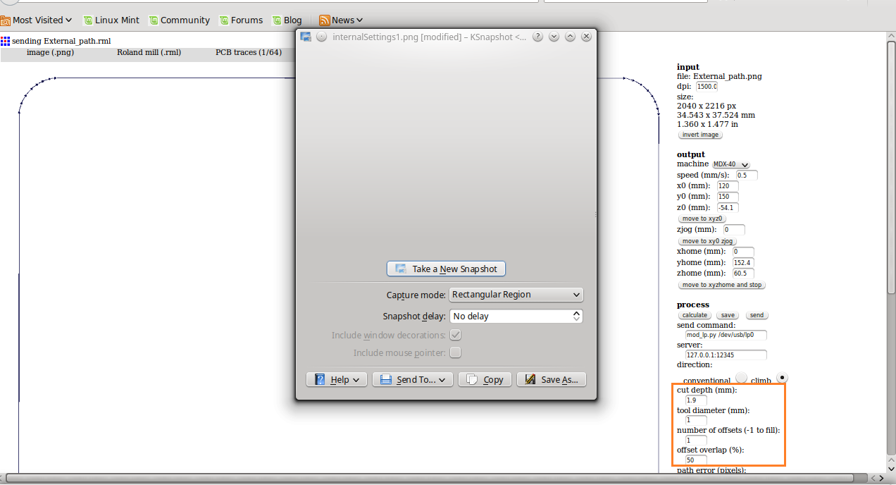
This time before milling, I checked if the right bed for my PCB production was there, a mistake pointed out to me by Neil on the week of Electronics Production. So, after the changing the bed, I went throught the same procedure as in the Electronics Production week. The settings for the internal path and the external path can be seen below:
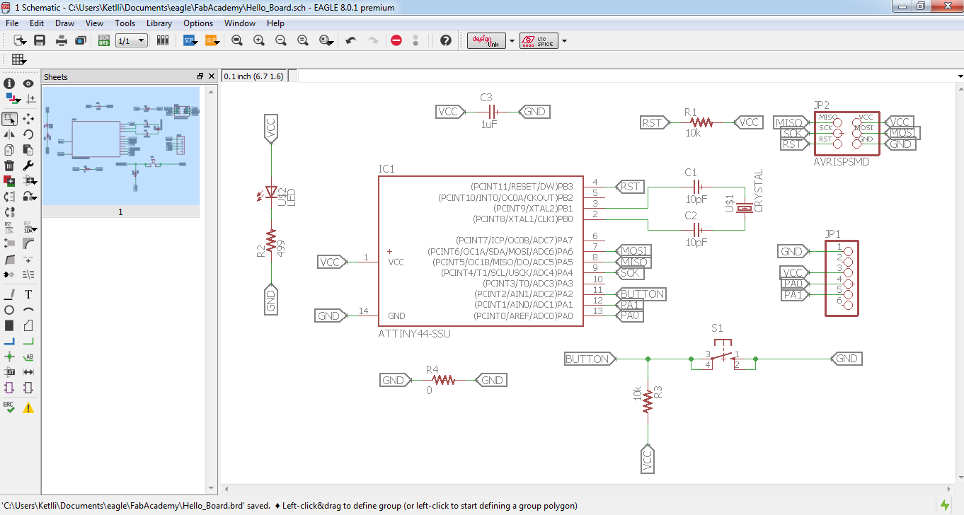
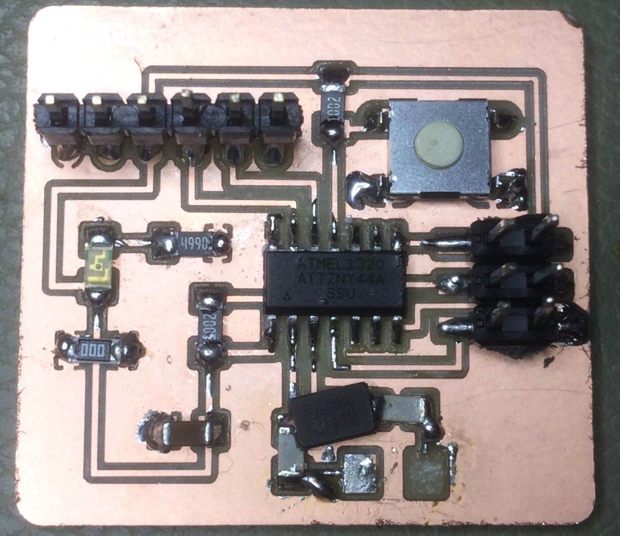
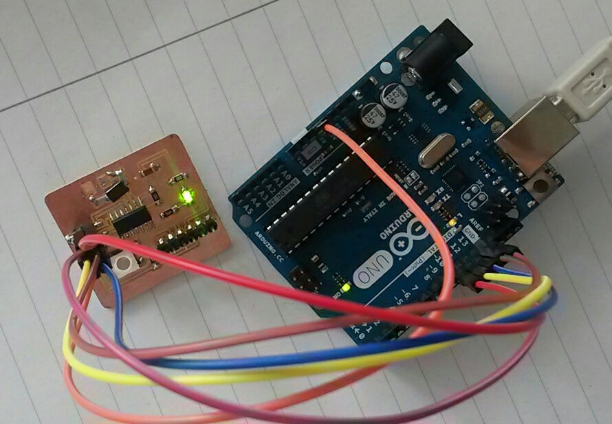
During the soldering, I tried to make the joints as shiny as possible. Also, as I mentioned before I realised my mistake of the place of the crystal after I finished the board. So, I tried to desolder the crystal and capacitors and just change their places. But while I desoldered one end of the crystal, I made a pad dissapear so I soldered the crystal before the capacitors and in a way above them. I know very rough and not beautiful way to do it but thankfully it worked and did not have to make another board and loose more material. :) Below you can see the result. After this I corrected my schematic and board on eagle. NOTE: The negative side of the LED goes always to the opposite side of the MCU pin if it connected to GND.
Programming
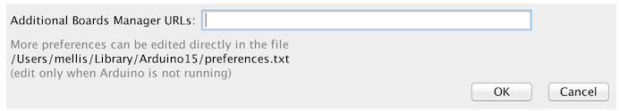
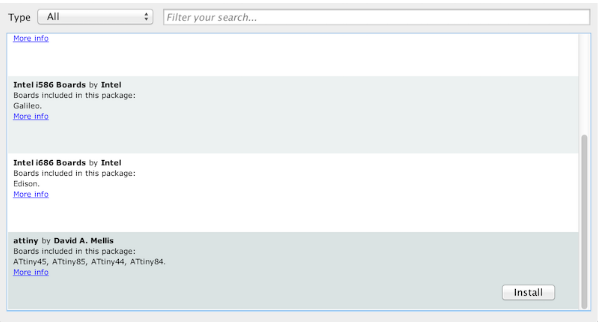
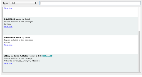
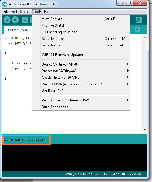
The first step to program the board was to patch the ATtiny 44 with Arduino ide. I opened the preferenes dialog on Arduino IDE, found the "Additional Boards Manager URLs" and pasted this URL into the field and pressed ok: "https://raw.githubusercontent.com/damellis/attiny/ide-1.6.x-boards-manager/package_damellis_attiny_index.json". Then, I opened the boards manager under board on the tools menu. After I opened it, when I scrolled down to the list I saw the entry of ATtiny, I pressed on it and installed it.
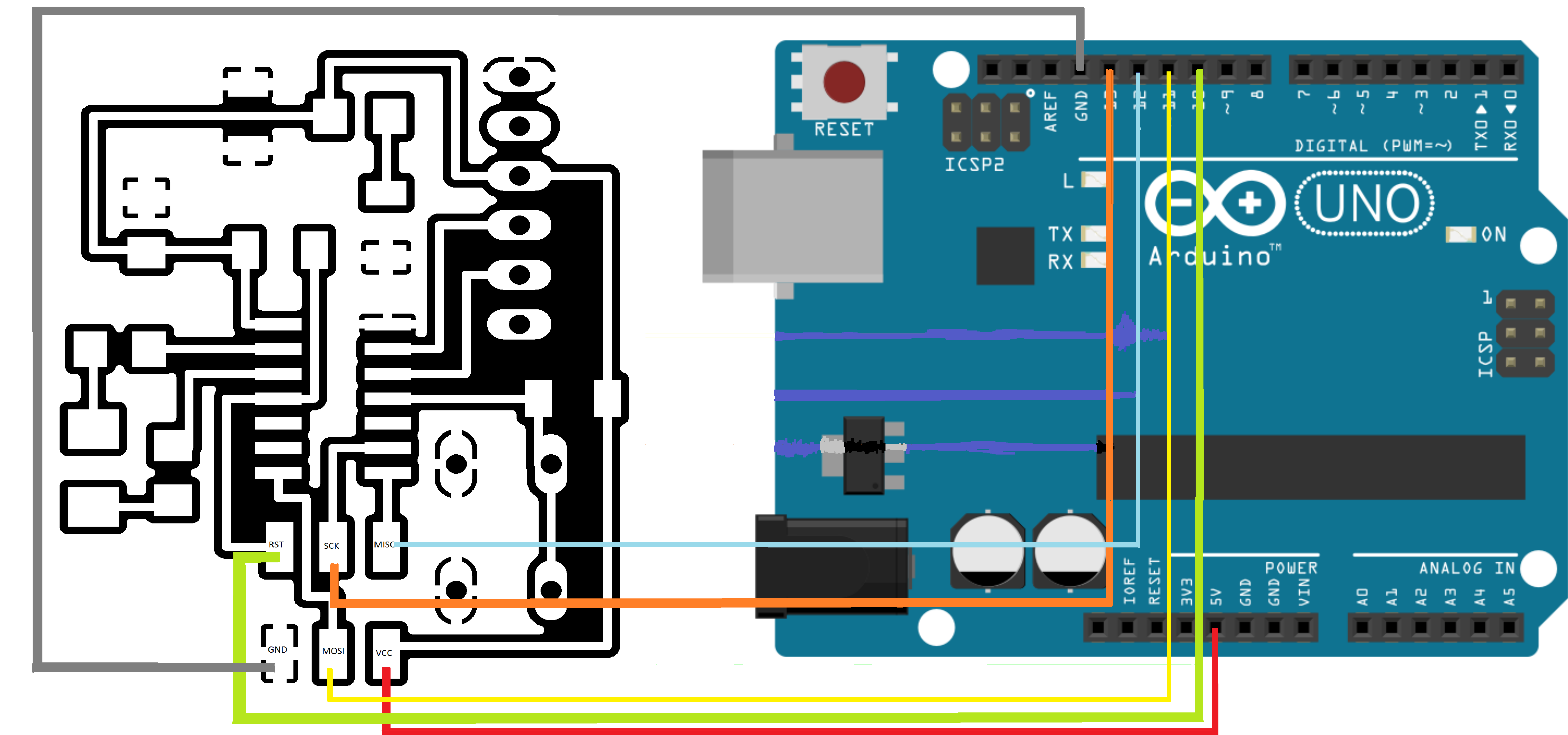
After ATtiny was patched, I started programming my board following these steps:
Downloads
The Schematic and the Board files of the Hello Board.
The internal path and external path files of the Hello Board for the milling process.