
2016
Rudrapalsinh Solanki
Week-15
Embedded Networking and Communications
Assignment
1. Make a wired connecting boards.
2. Design and build a wired &/or wireless network connecting at least two processors
I Decided to work with node system for this exercise.
I will code the board with arduino programming through C/C++ language.
So I designed a pcb with the attiny 45 and then see the connection of 3 boards with each other.
Now its turn to design the board in Eagle design and start working with it.
Steps involved are :
1. Design the board with the required components
2. Milling the board
2. Soldering the components
3. Programming of the board through Arduino
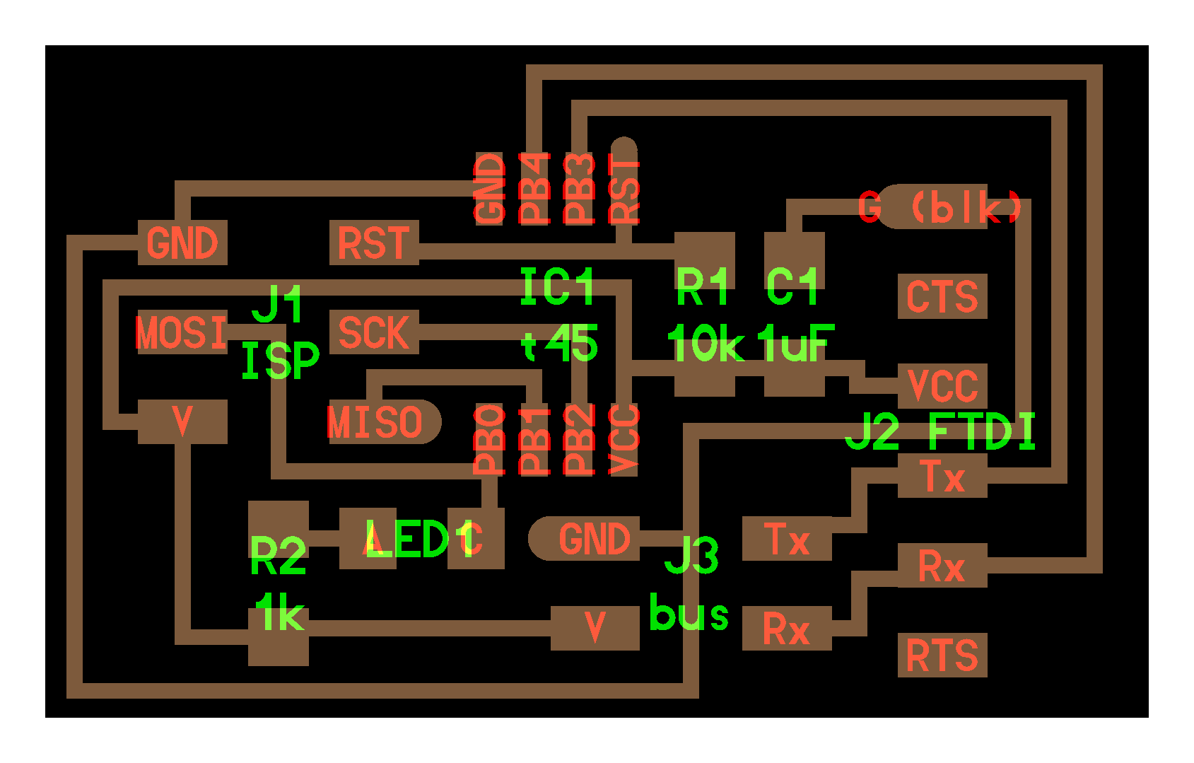
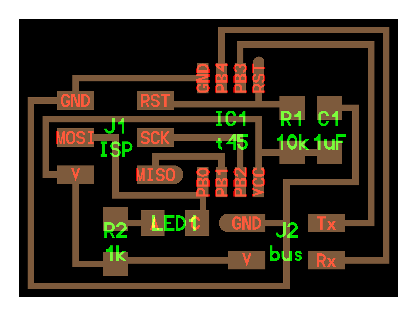
1. Design the board with the required components:
.jpg)
.jpg)
.jpg)
.jpg)
.jpg)
.jpg)


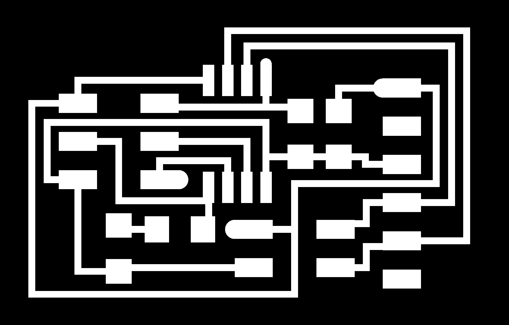
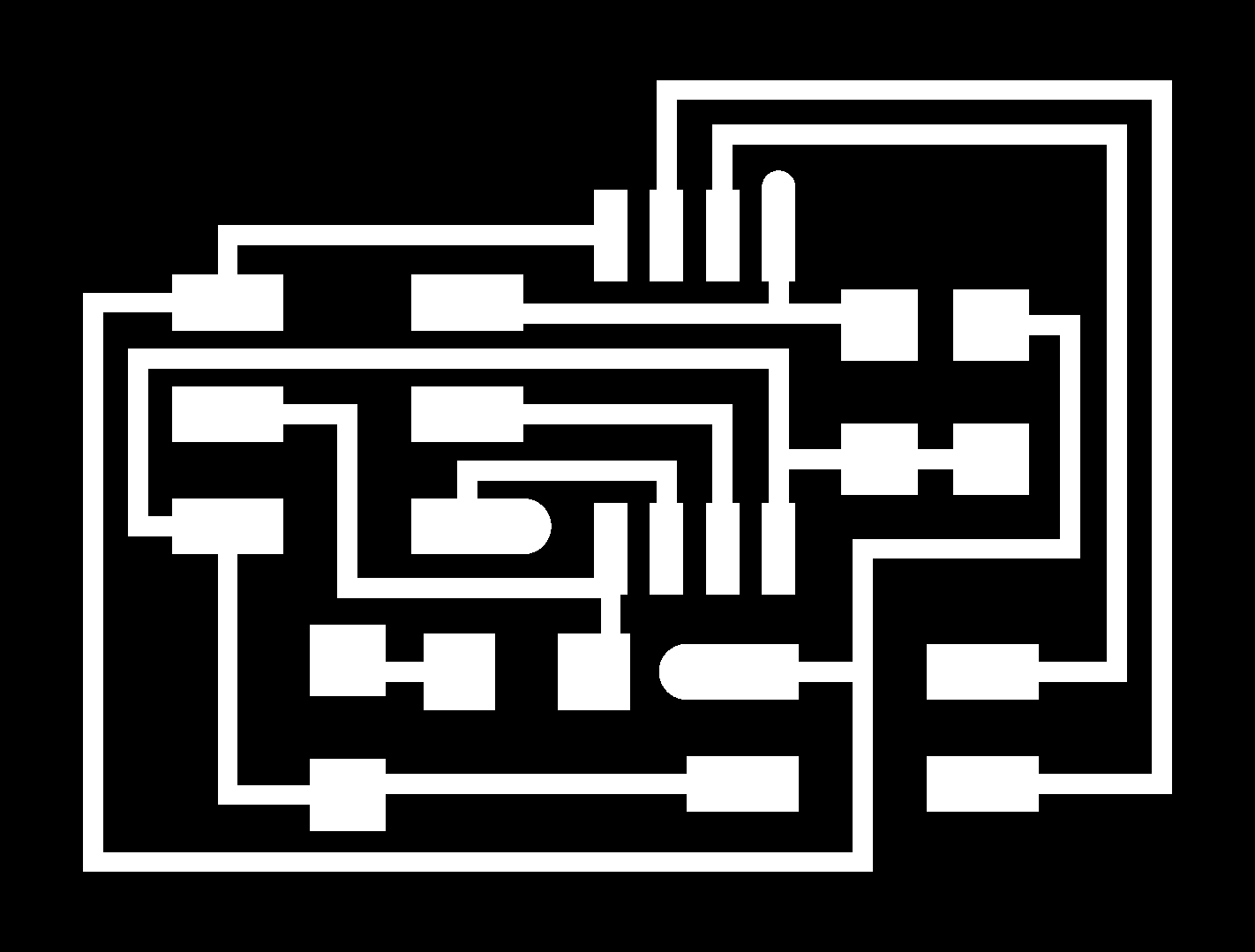
This the png created from the eagle now invert the image to get the final image
Png file for the bus download
.jpg)
%20copy.jpg)
This the png created from the eagle now invert the image to get the final image
Png file for the node download
-copy.png)


2. Milling of the board:
First the circuit traces are cut with 1/64 bit


Once the circuit is milled now the board in cut with 1/32 bit


.jpg)
3. Soldering all the components on he board:
Final milled boards


For this assignment, I printed the boards and milled them using the fab module. The link to download the file is LINK.
I selected to make Hello Bus 45 Bridge and Hello Bus 45 node system. The board was milled using ROLAND MODELLA from the fab academy archive page. The traces of the board was taken into the fab module and was milled in modella milling machine. 1/64 th drill bit was used for the first traces of the circuit board.
Asynchronous serial bus and node system


STEP_01 The png file of Hello Bus 45 bridge is loaded into modella

STEP_02 Once the png file is loaded the 1/64 mill trace tool is selected and the make file is made.

STEP_03 The z is set and the make file is transfered from png to rml and the xy is set and the board is ready to mill.

STEP_05 The z is set and the make file is transfered from png to rml and the xy is set and the board is ready to mill.


STEP_06 Once the milling of the circuit is done will have this screen successfull and than press exit and load another png file.

STEP_07 The png file of the other Hello Bus 45 node is loaded into modella

STEP_08 Once the png file is loaded the 1/64 mill trace tool is selected and the make file is made and than the zero is set and the png file is made to rml file.

STEP_09 Once the tracing of the board is done than the circuit is ready to cut. 1/32 inch bit is fixed and the cut path is loaded in modella through a png file.


STEP_10 Once all the files are loaded and cutted then it is ready for soldering.


STEP_11 The board is removed from the big sheet and cleaned with the water paper.


STEP_12 Bridge and the node board is ready for soldering.


STEP_13 I achieved failure almost 5/6 time soldering the circuit for both the boards. These are the boards that were all the failure of my soldering. Iwill still once more than I will be able to programme it.


STEP_14 I finally started coding once I have made all the boards now. Initially I first took the arduino board and connected to the computer and uploaded the arduinoISP code in the board.
Steps of uploading the code on arduino LINK


Code for uploading on arduino LINK


STEP_15 Upload the code in all the 3 boards. First take a hello bus.45 bridge and upload the code in the board. I had done a small mistake in fixing the led in this board so I replaced the LED and fixed another light but not the smd one.
After the code is upload use the same technique to upload the code on the 2 nodes and the working of the board will be seen through the blinking of red light.
STEP_16 Open the Arduino software in your computer and see the result clicking on the serial monitor.
It sends the signal from your computer to the bus to nodes and the light blinks.
Week 15 Files