Week 7: Electronics Design
This week's tasks:
- Group assignment:
- Using the test equipment in our lab to observe the operation of a microcontroller circuit board
- Link to the Group Assignment Page
- Individual assignment:
- Redrawing the echo hello-world board
- Adding (at least) a button and LED (with current-limiting resistor)
- checking the design rules, making it, and testing it
Challenges:
- Working with Eagle was initially a bit challenging for me. Especially moving grouped objects :-D But at some point, I started to enjoy the program and the schematic creation process. And good to mention thanks to Antti's workshop
- Eagle again, in the stage of creating the traces of the board, I had to re-create the routes in a way that they do not overlap. It was like solving a puzzle, which is not my favorite choice. So I could say quite challenging at the moment. But seems fun later on when you have nothing else to do but just thinking about it.
- Soldering was challenging for me again since the components were really tiny and detailed but it was kinda cool. Moreover, for some components it was a bit difficult to figure out how to adjust it in the right side.
- Surprisingly my programmer from week5 (electronics production) did not work this time. So I used my friend's programmer to test my board.
Ps. I fixed the problem with help of Ivan (one of the fablab instructors). I explained the reason at the end of this page. So eventually I programmed my own board with my own programmer and my own computer
Considerations:
- Good to remind to download fab.lbr file to a place that would not disappear in case of updating.
Technology Used:
- Eagle
- Fabmodules.org
- Soldering
- Multimeter
- PuTTY
Eagle Settings and Library Management
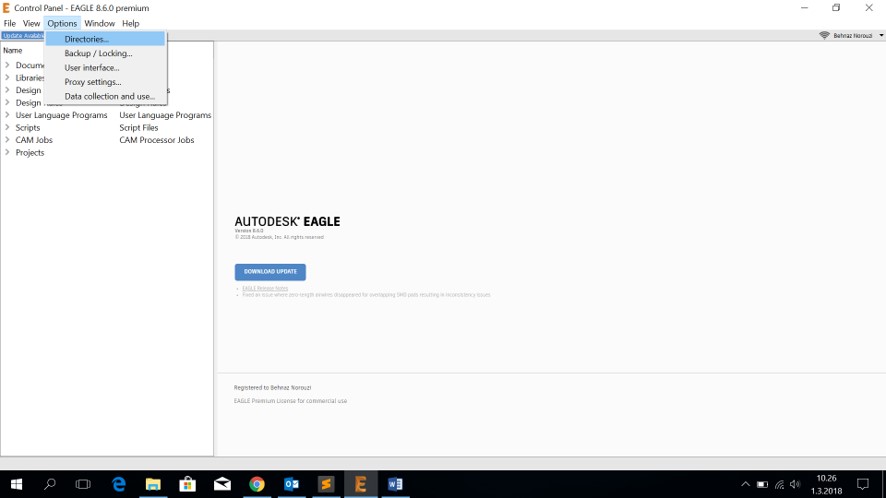
Through Antti's workshop I downloaded and installed Eagle for the purpose of designing the schematic of the circuit.
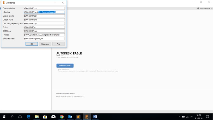
- Downloading the library including the fablab components named 'fab.lbr' from Electronics Design page. It is necessary to download fab.lbr file to a place that would not disappear in case of updating.
- Eagle > control panel > options > directories
- Copy the path that fab.lbr is in, here
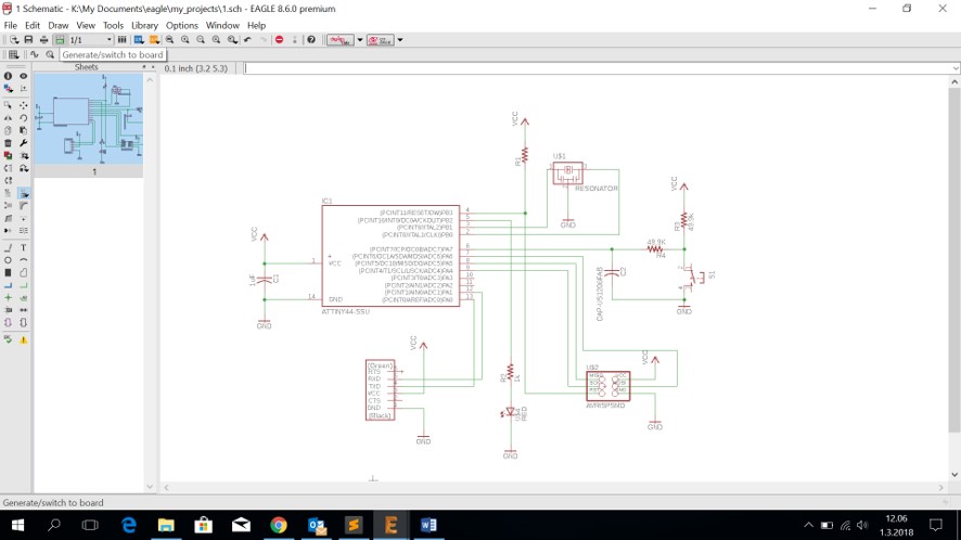
Creating the Schematic of the Board
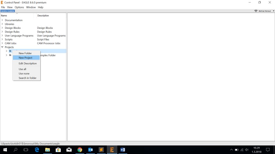
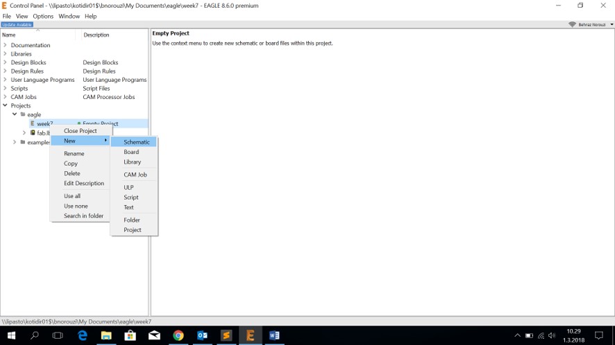
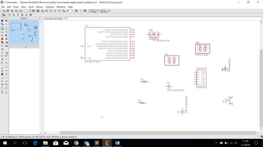
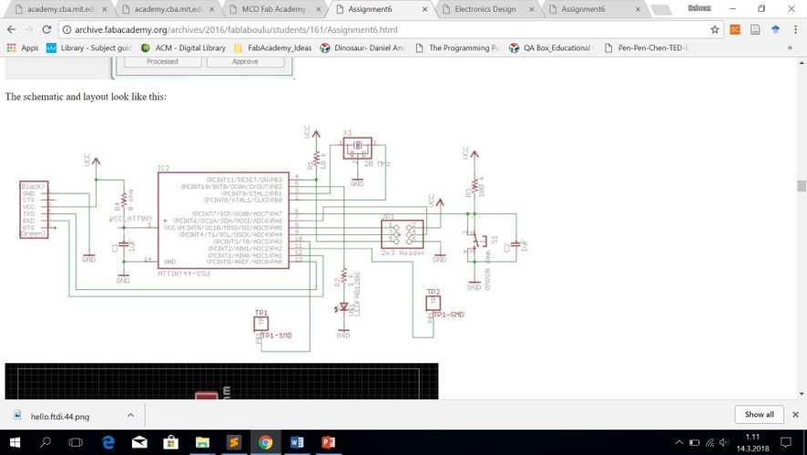
We needed to figure out the components and the logic of the connections of Hello ftdi 44 board.- Create new project: Opening Eagle > Project > eagle > Right Click > new project
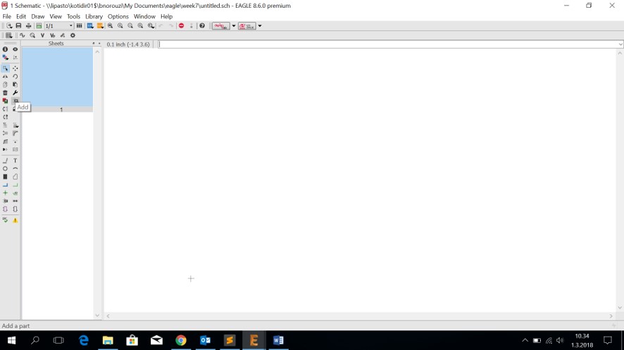
- Create new schematic:
Activate the project by clicking on the circle in front of it.
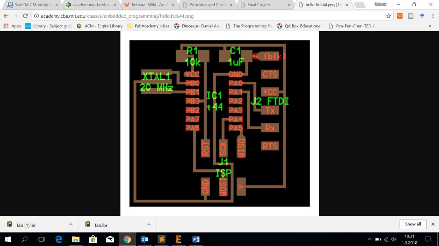
Then: right click on the project name > new > schematic - Open the hello.ftdi.44 board from fabacademy page.
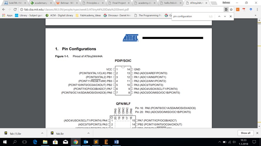
- Google attiny44 datasheet. Open the document and find the pin configurations.
- Now it is time to add components.
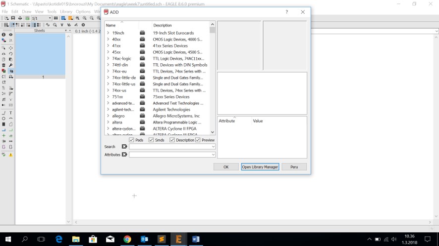
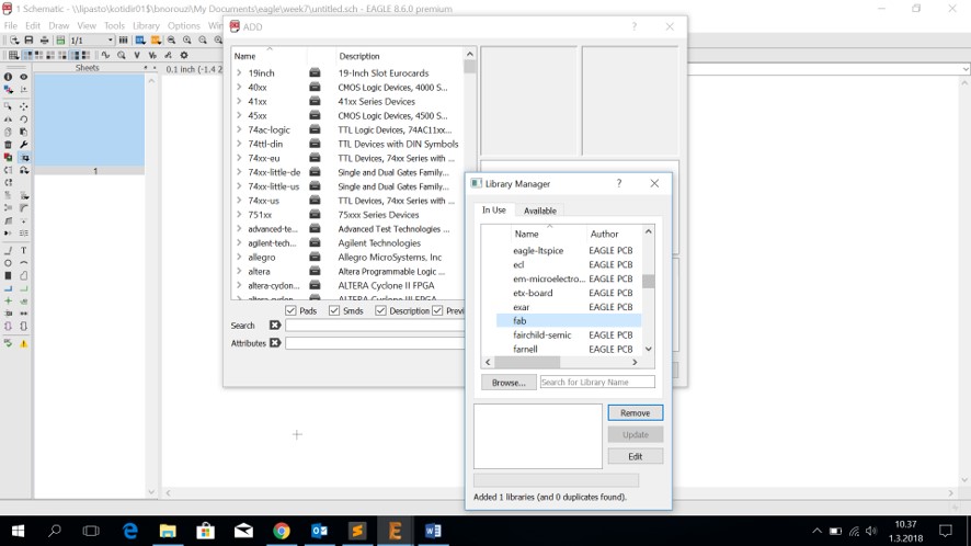
- Hit 'open library manager'.
- Browse and open fab.lbr (we saved it previously as I explained before).
- Now here we have the fab library.
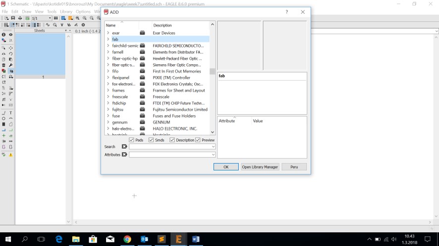
- Add all the components that we need from the fab library for making Neil's hello.ftdi.44 board. These components are drawn for manual soldering. Following Antti's recommendation, we also added a filter that would remove the bouncing from the button.
- I checked Antti's page for checking how the schematic should look like and to make the connections using 'Net' tool.
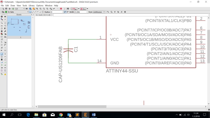
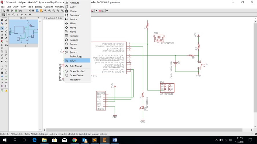
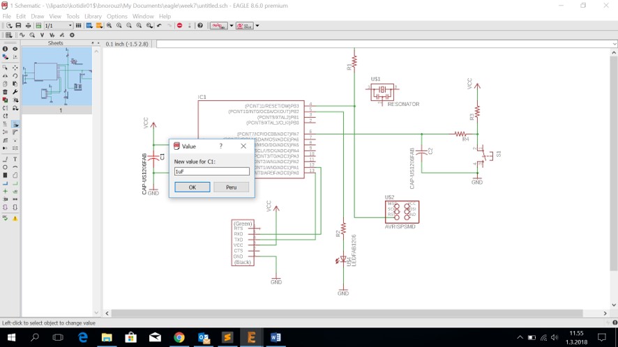
- Then I set the values by: right click on the component > value > set the value
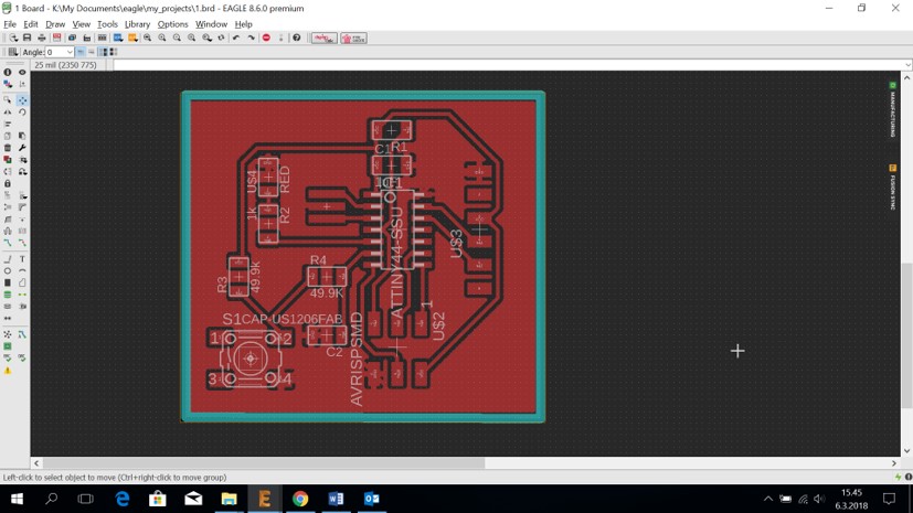
- And finally the schematic design of the board is done

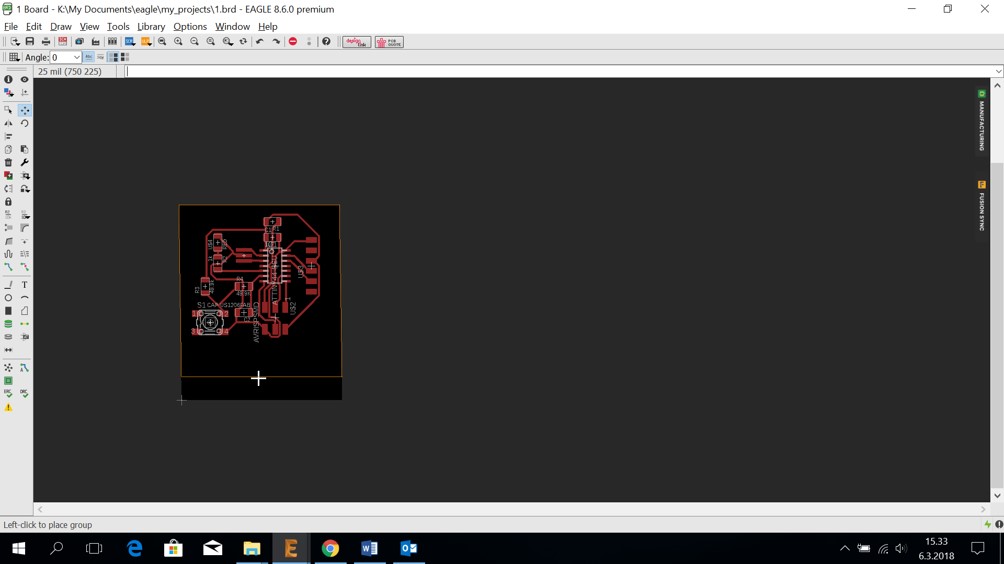
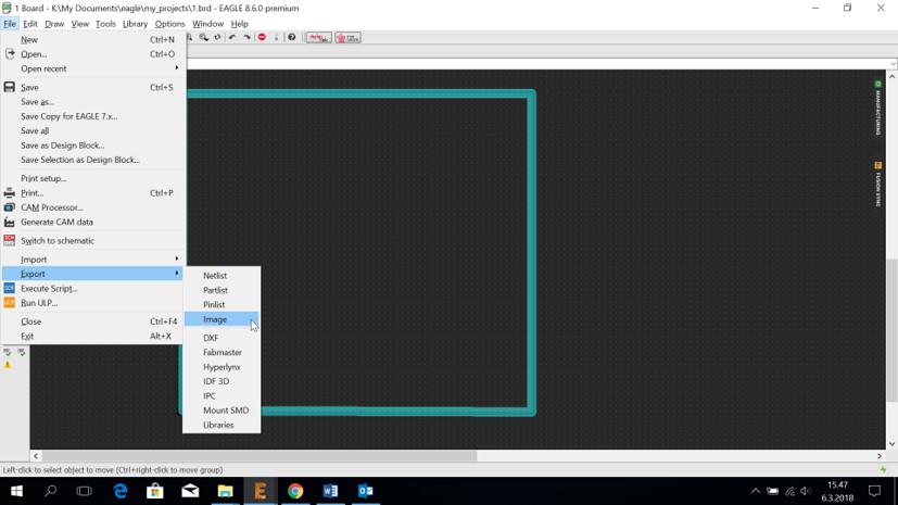
Creating the Traces of the Board
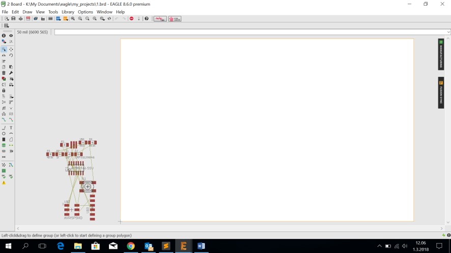
- First, we hit 'Generate/switch to Board' for generating the board.
- The board will be generated.
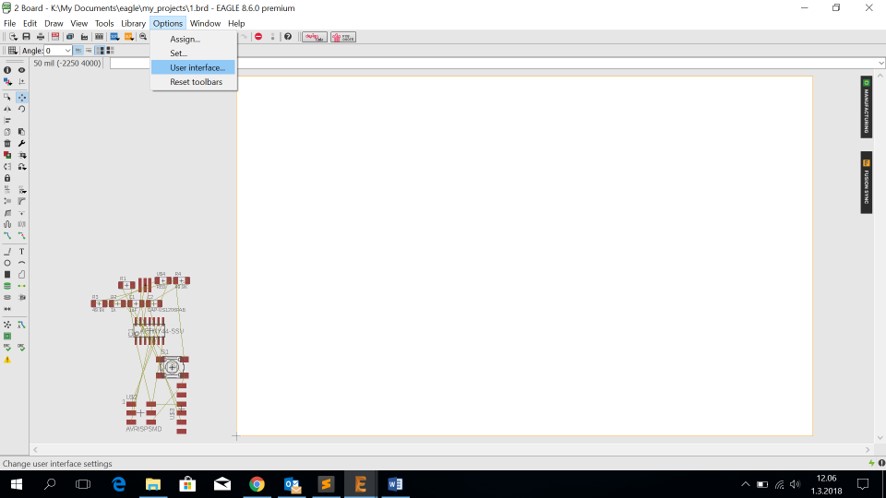
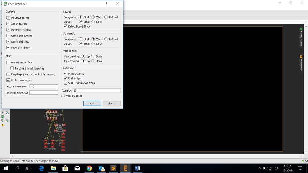
- We made the background black: Option > user interface > background > black.
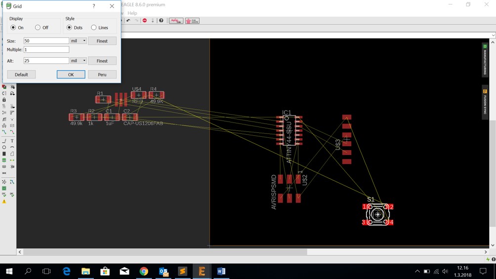
- We also changed the grid setting. EAGLE forces the parts, traces, and other objects to snap to the grid that is defined in the size box. It was 50 mil by default. We changed it to 20 mil.
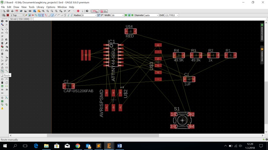
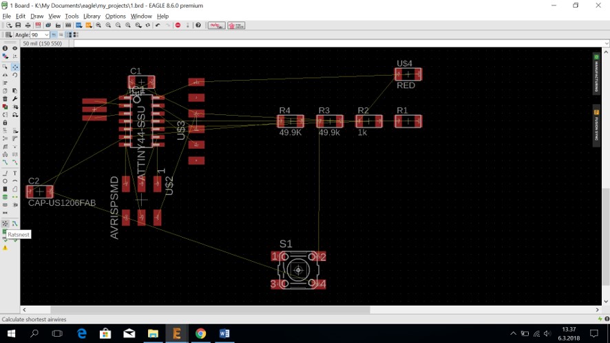
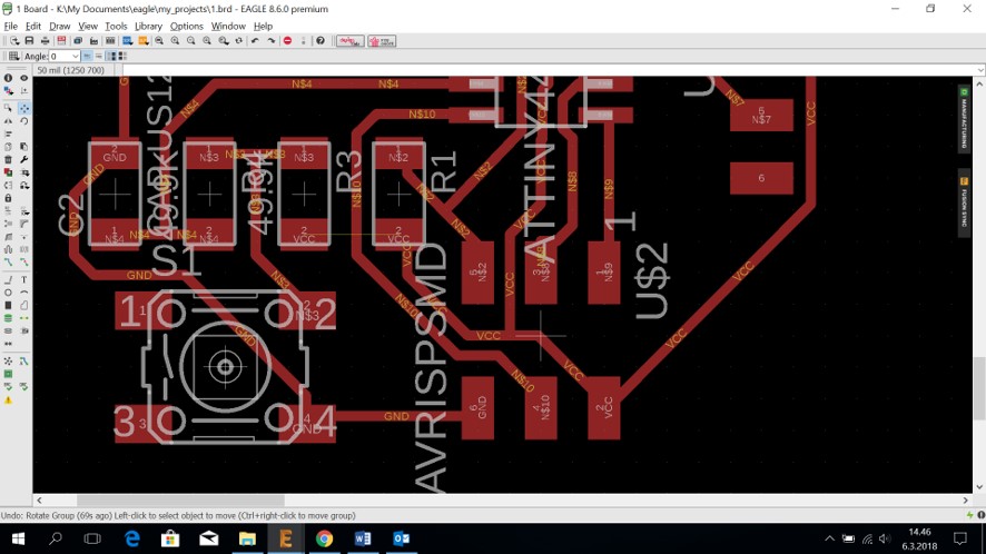
- Now it is time to create the routes. The routes should be created in a way that do not overlap. We simply used Edit > move and Edit > rotate for positioning the components. And we used Edit > route for making a route from a component to one another.
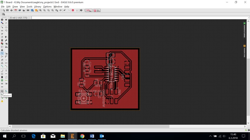
- We used Tools > Ratsnest for identifying the airwires and recalculating the distance of the lines.
- When I was moving the components I used to press alt key for keeping symmetry.
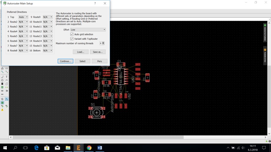
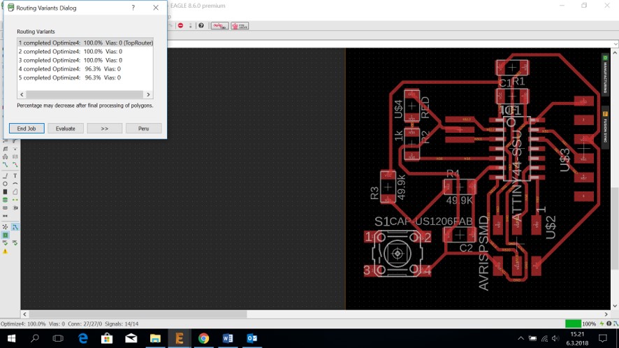
- The main setup for autorouter: Tool > Autorouter; Set the top > Auto and set everything else to N/A.
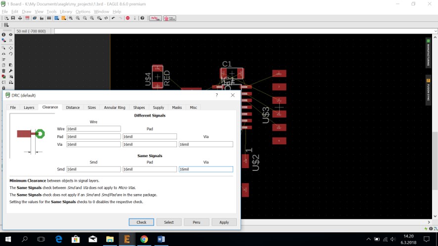
- I also changed the default of DRC and set everything to 16.
- As a result: I have a wire from R1-R3 crossing another one and I should find a way to replace it in a way that wires do not overlap each other.
- I was like a puzzle difficult to find a way. So as one of my friends suggested, I started by unrouting all the ground lines and then I changed the routes and finally solved the overlapping problem.
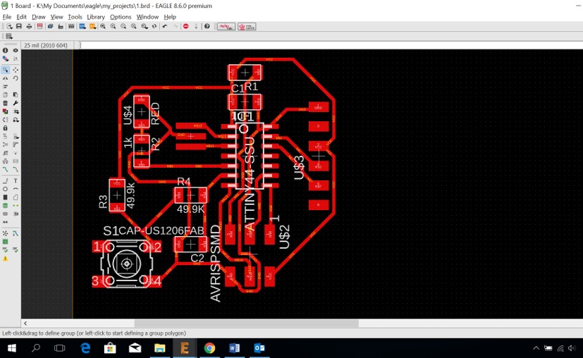
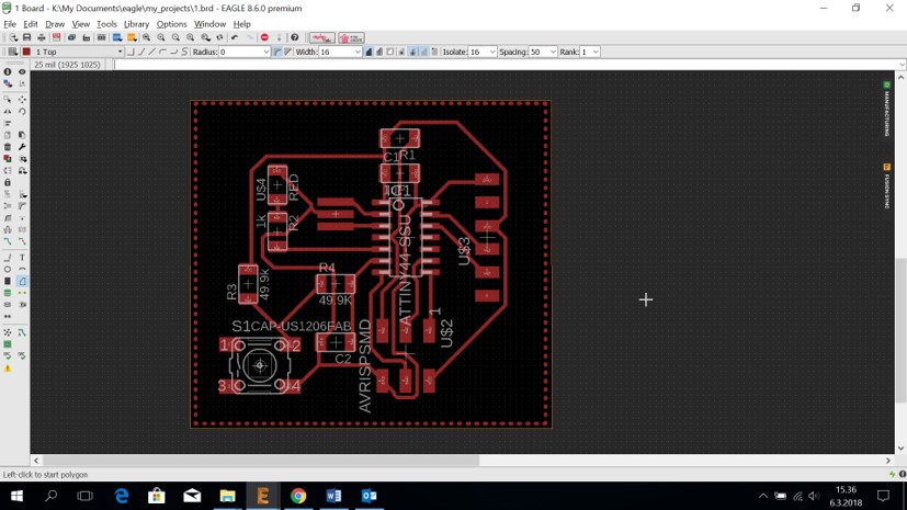
- I resized the screen around the board size.
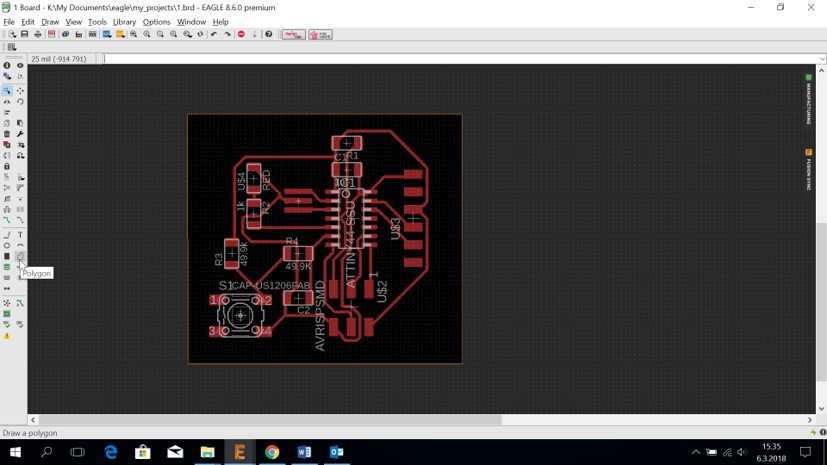
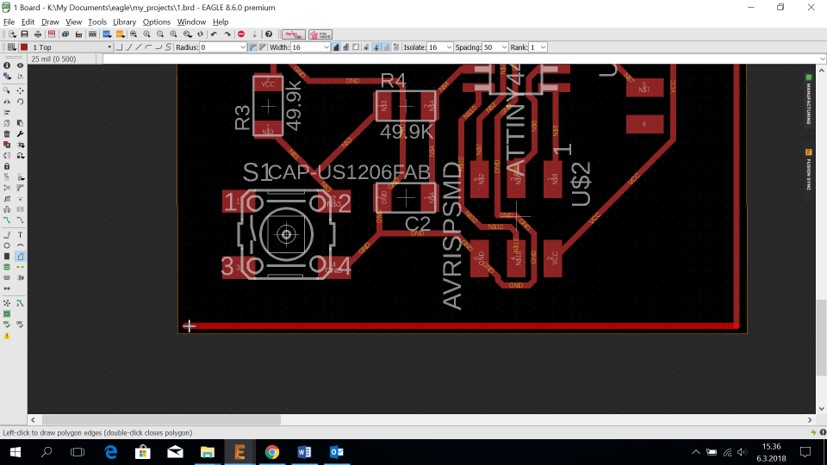
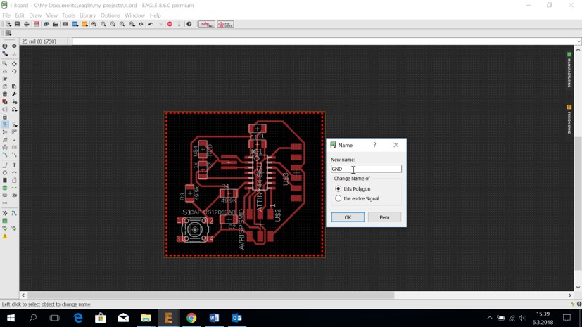
- I used 'Polygon' to fill blank space on a PCB with copper connected to ground. I show how I did it by:
Drawing a polygon using polygon tool around the pcb
Naming it as GND
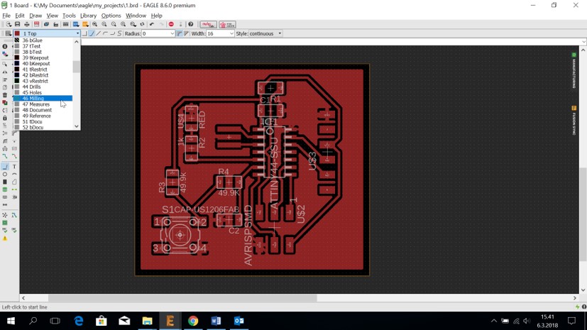
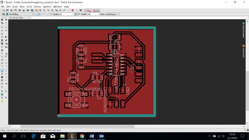
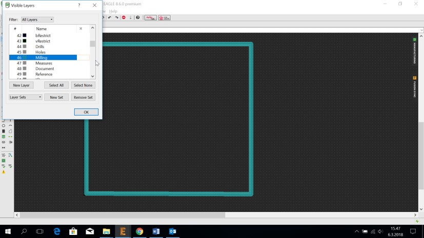
Selecting Ratsnest - I drew the outline of the cutting using line tool and choosing 46 milling.
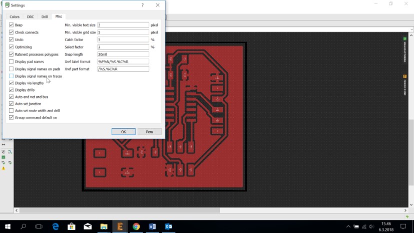
- Then I changed the settings for exporting the image:
options > set > Misc > unchecking the following:
Display and Names
Display signal names on pads
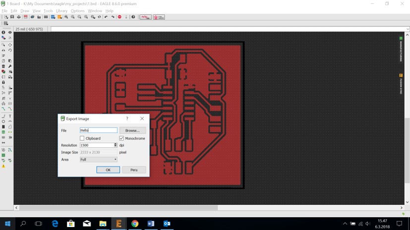
Display signal names on traces - Exporting the image of the traces:
Layer setting > hide layers and slecting only top view
File > export > Image:
resolution:1500 dpi
Monochrome - Exporting the image of the outline:
Layer setting > hide layers and slecting only 46 Milling
File > export > Image:
resolution:1500 dpi
Monochrome
Milling and Soldering
I have explained the process of preparing files for milling, the process of milling and also the process of soldering in Week 5's Assignment, So I here just upload some pictures as the results:


Testing
Testing with Multimeter after soldering for checking continuity. And everything was fine.

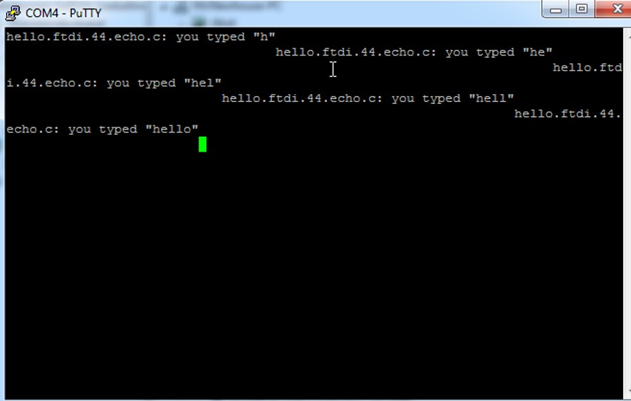
There was a problem with my computer at that moment of testing so I did the testing using the computer of one of my friends. Also my programmer from Week 5's Assignment that used to work previously but surprisingly it did not work at that moment. So I also used my friend's programmer to test the board. I followed Brian's documentation for testing.
- Connecting the board and the programmer.
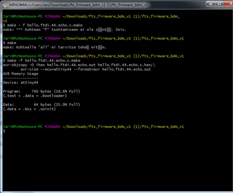
- 'make -f hello.ftdi.44.echo.c.make' command for making .hex file for flashing.
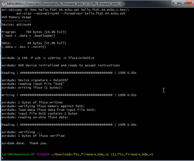
- 'make -f hello.ftdi.44.echo.c.make program-usbtiny-fuses' command for setting fuses
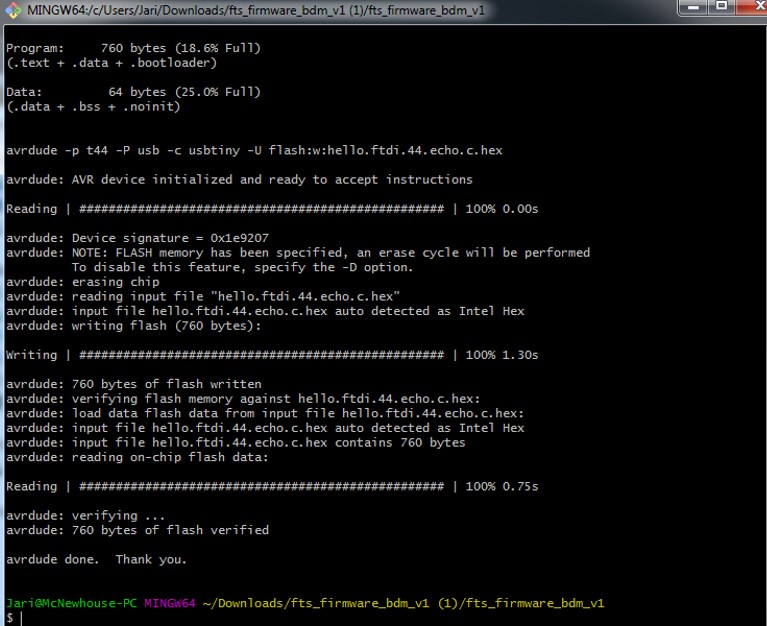
- 'make -f hello.ftdi.44.echo.c.make program-usbtiny' command for flashing the microcontroller
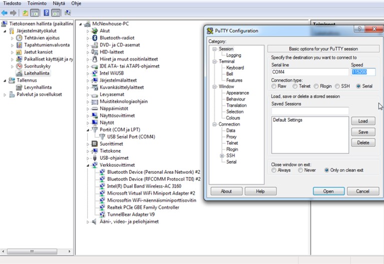
- In PuTTY configurations I configured:
serial line to COM4
and the speed to 115200. - It successfully echos what I type through PuTTY terminal.
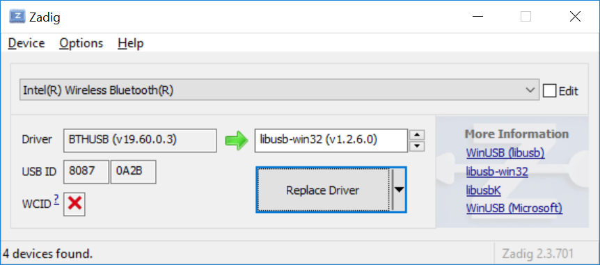
- I fixed the problem with my programmer and I programmed my borad with my own programmer eventually.
The problem was that everytime that I turn my computer on, for some reason I should go to Zadig and set the driver again. It automatically reset!


Original Design Files
RML File for OutlineRML File for Traces
Schematic of the board (.sch)
The board (.brd)