Redraw the echo hello-world board, add (at least) a button and LED (with current-limiting resistor), check the design rules, make it (if you have time this week, test it).
optional: simulate its operation. Measure its operation
Learning outcomes:
1)Select and use software for circuit board design
I decided to use Eagle PCB software, I select this software because it is a new software for me, also I saw than this software has a library of Fab Academy.
2)Demonstrate workflows used in circuit board design
Have you:
3)Shown your process using words/images/screenshots
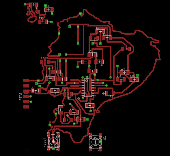
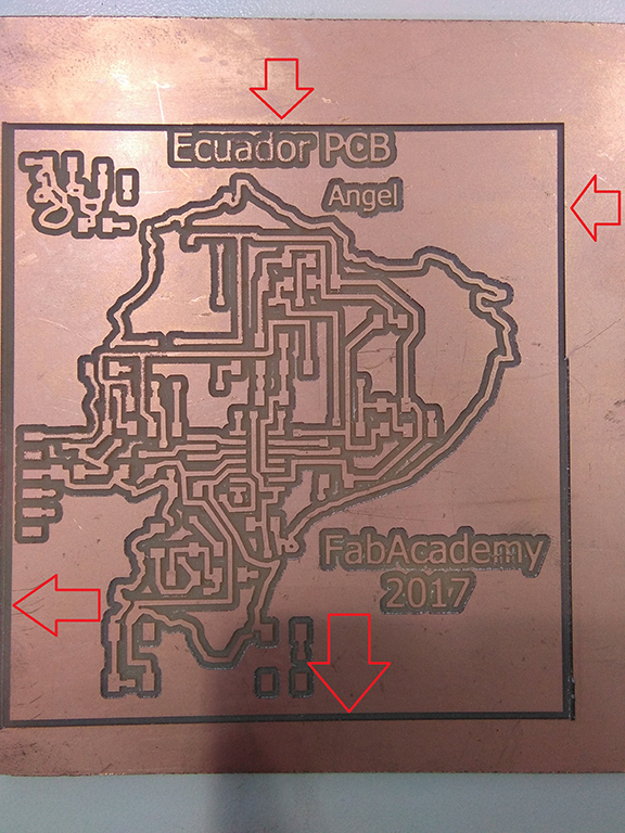
In this assignment I decide to create my own file, I have some idea to create a PCB, but I decided to do the Ecuador map.
The idea is create a PCB drawing a map.
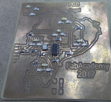
The objective is turn on sixteen led lights using five pins, the technic to make it is called charlieplexing.
The software to create the PCB is Eagle PCB, I used the fab.lbr.
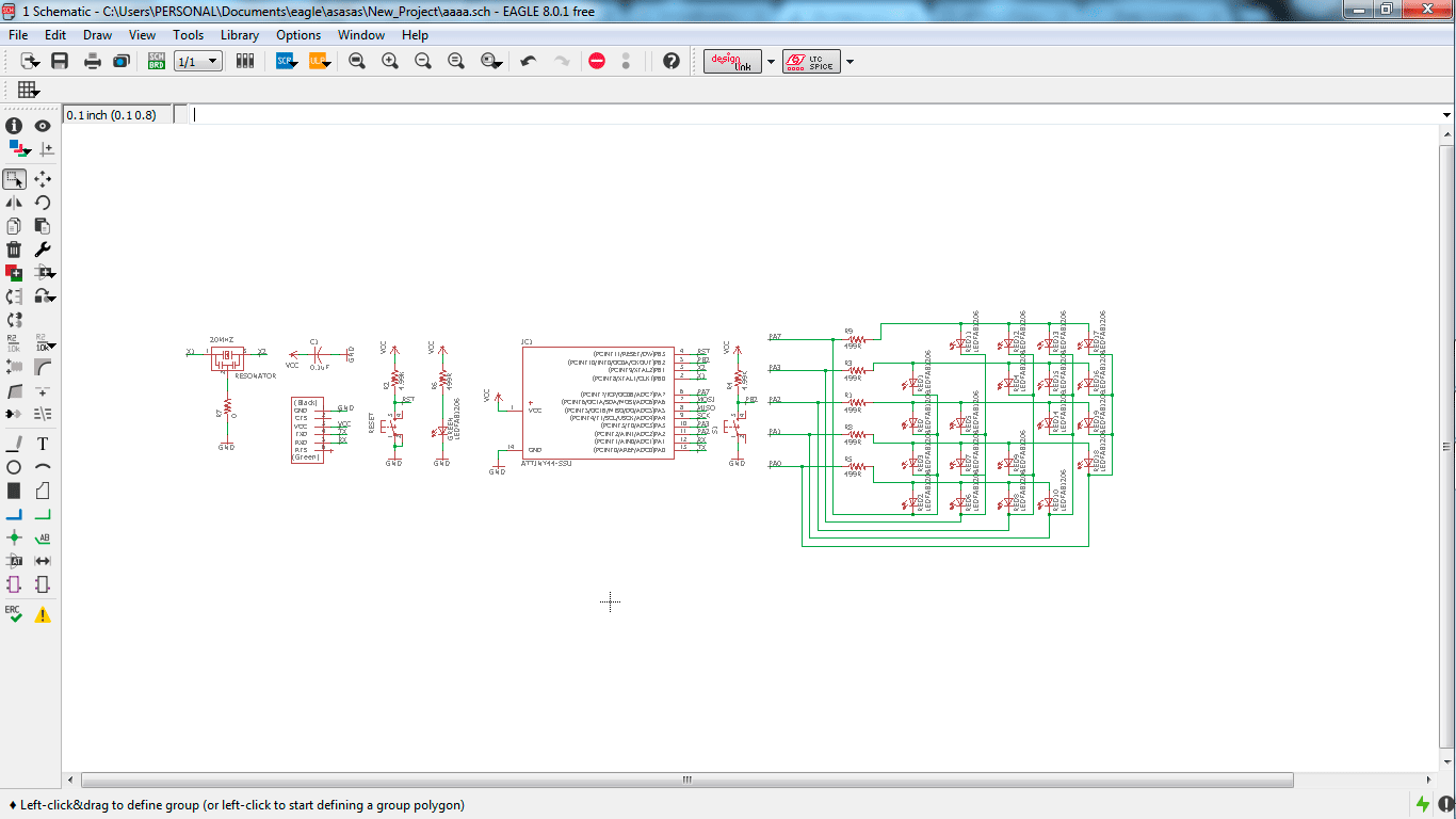
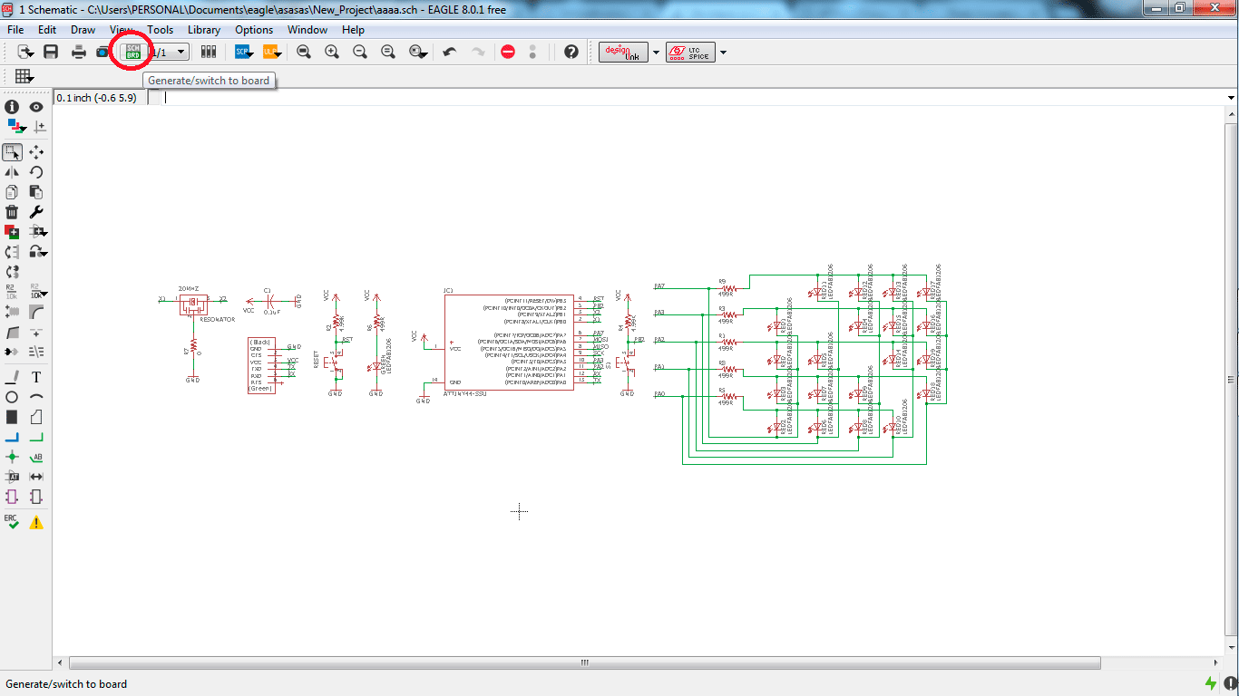
The first step is create the schematic
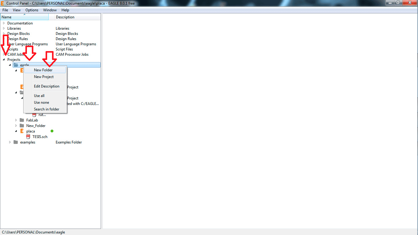
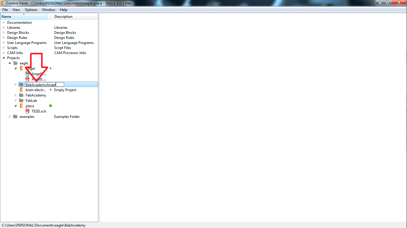
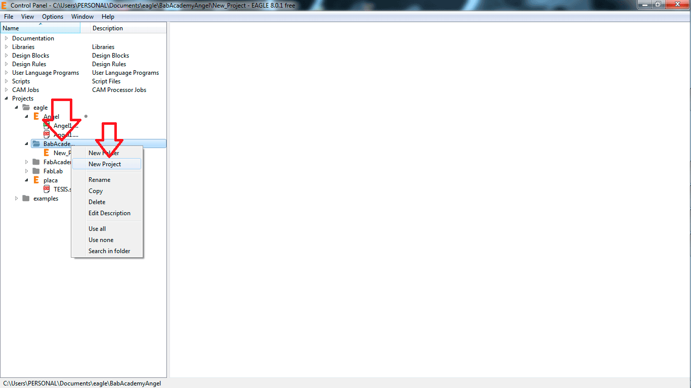
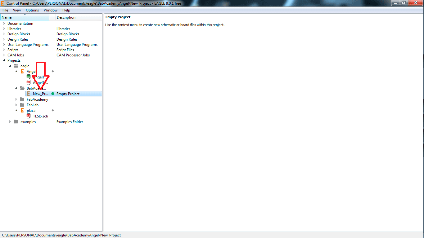
I created the file in Eagle PCB, we have to create a folder, then a new project inside the folder and finally the schematic file.
you can see how to make it in the next pictures.
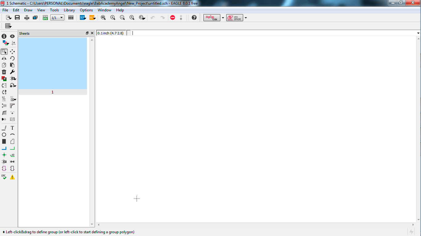
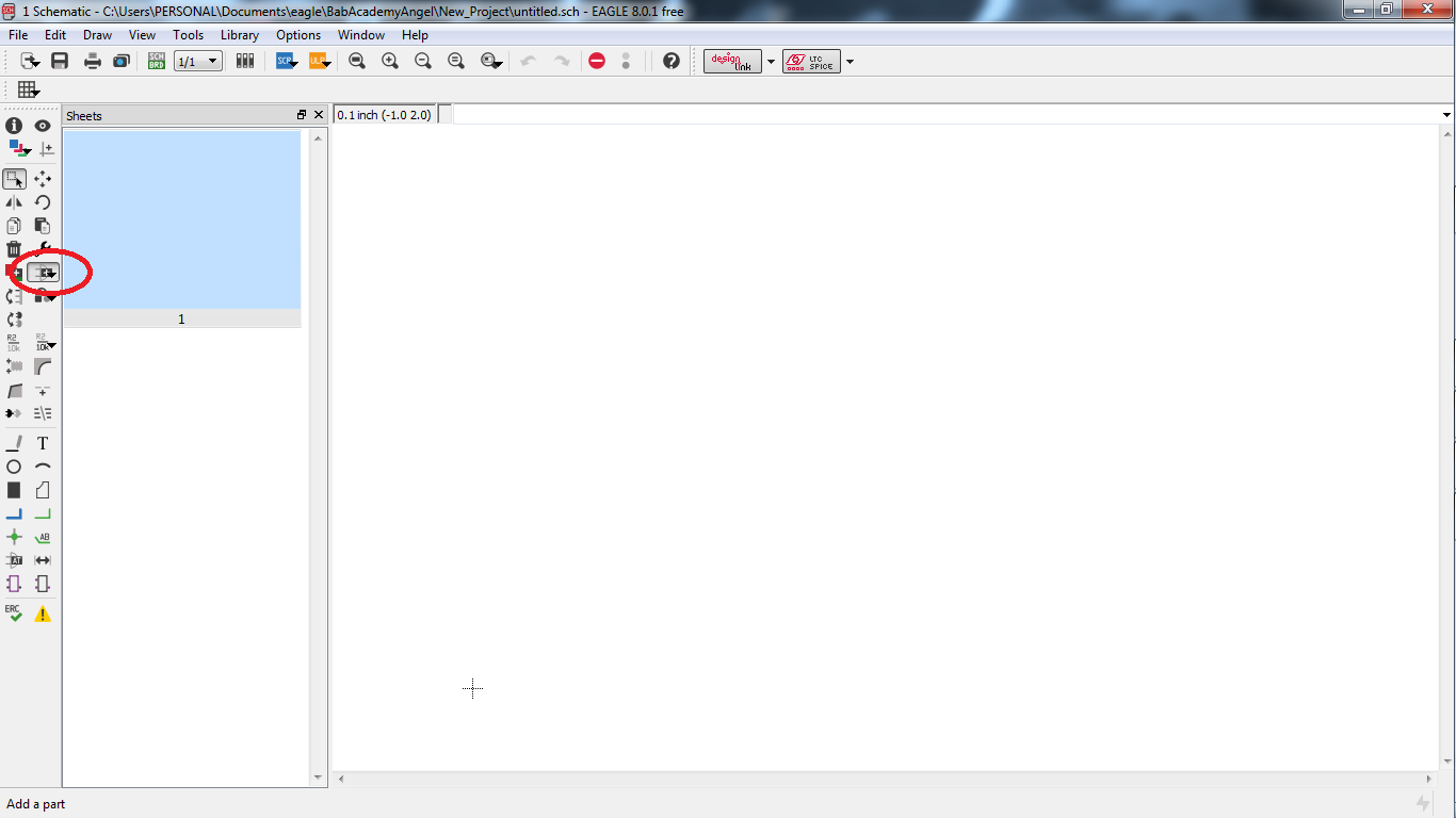
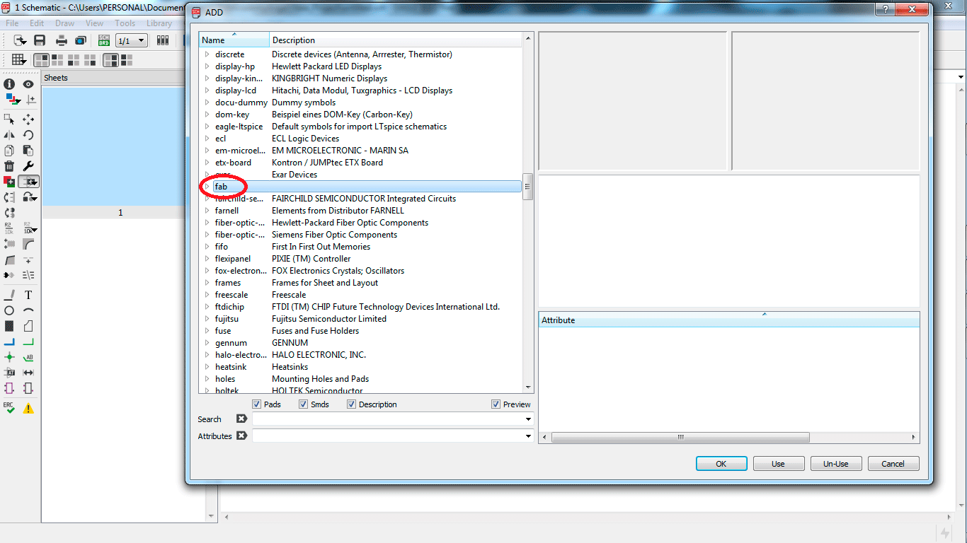
In the schematic window you can add the components and select all the library Fab.
In this window you can choose the library than you want, in this case I use the Fab library.
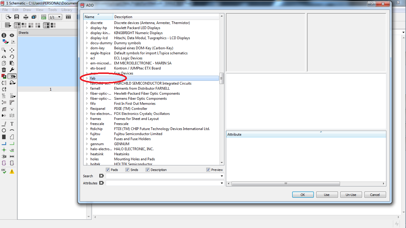
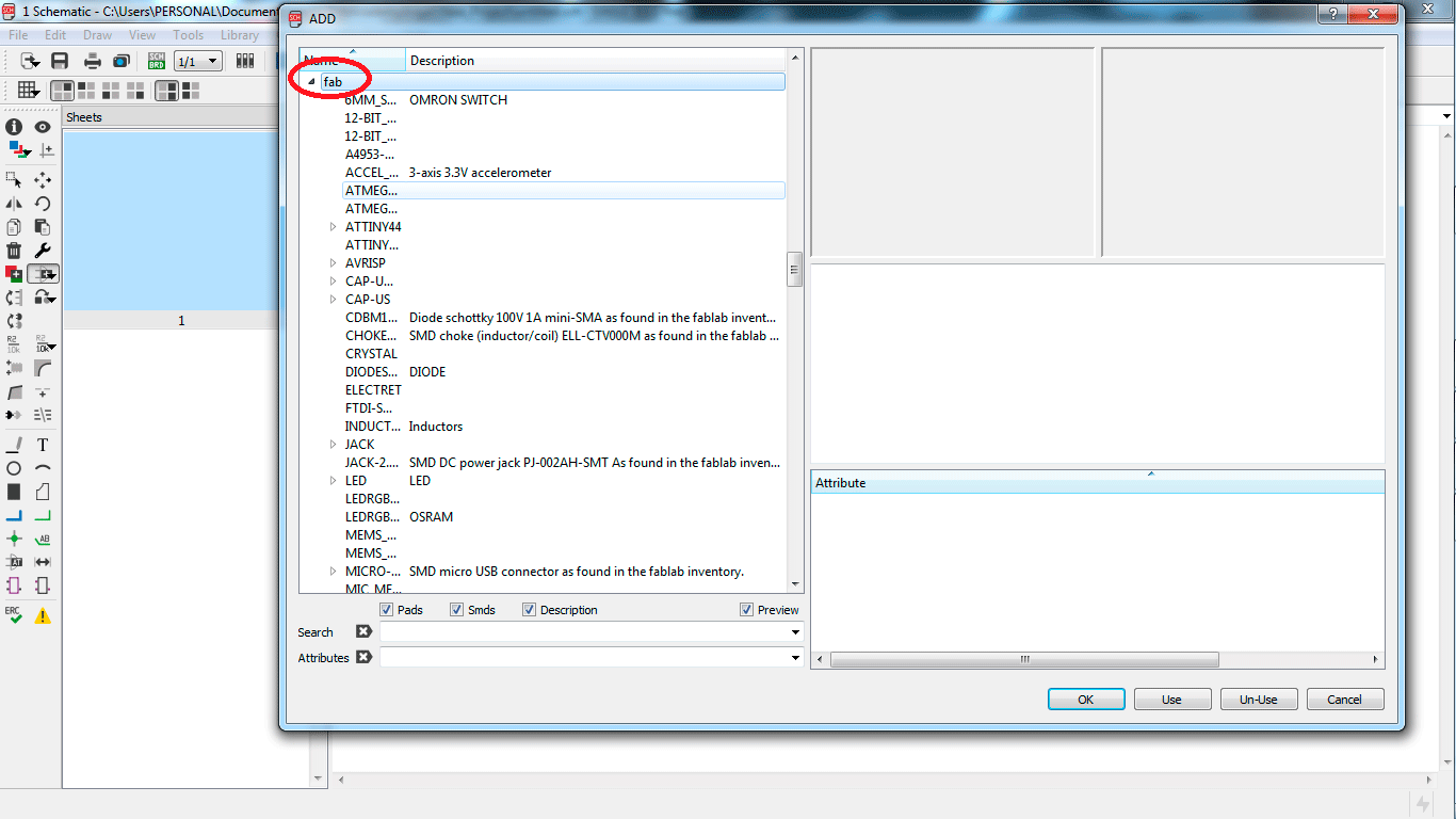
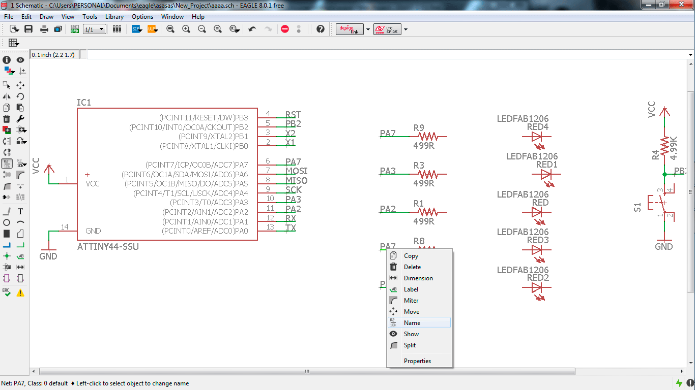
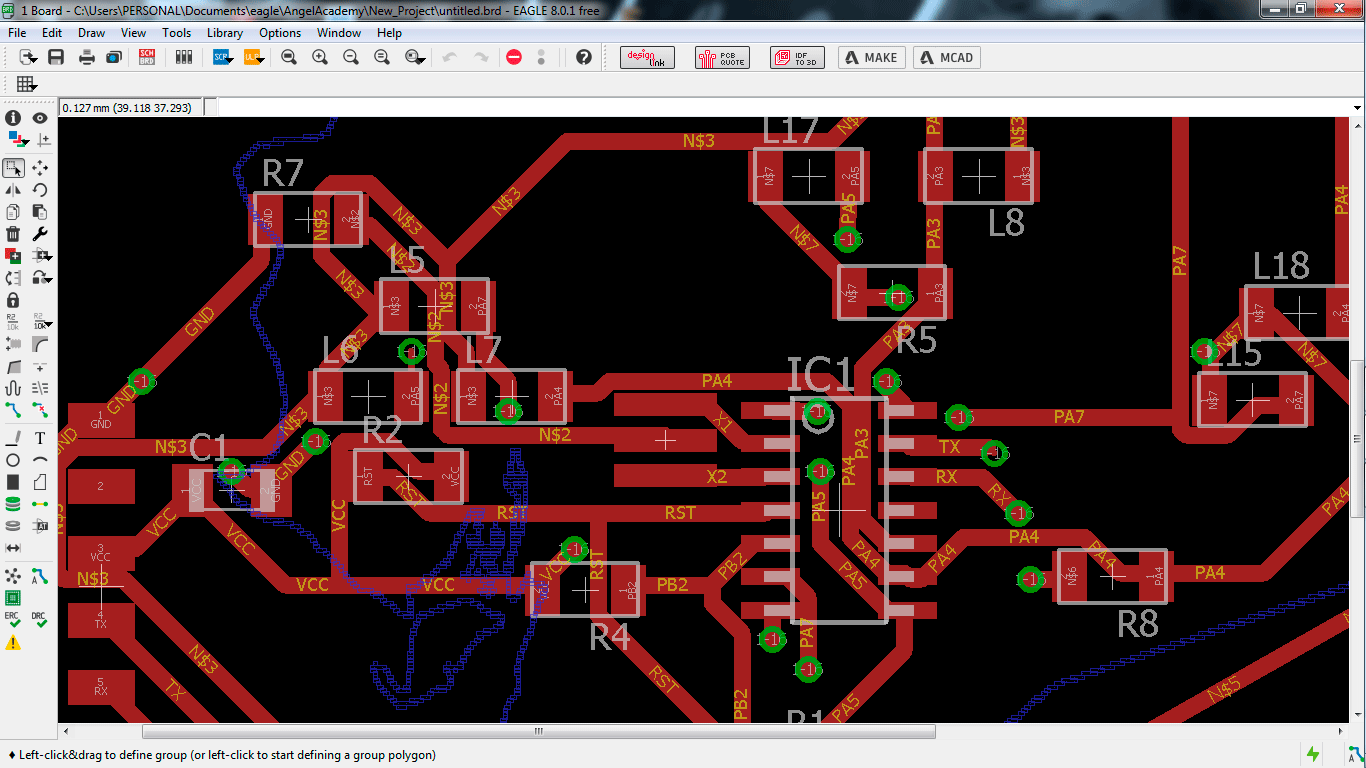
I chose all the components than I needed and I did the schematic.
If do you want to know all the components than I used, you can download all the files in the final of this page.
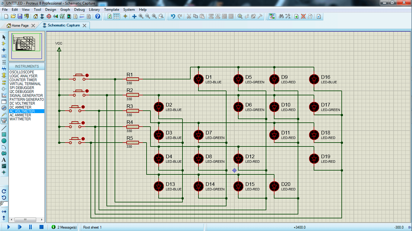
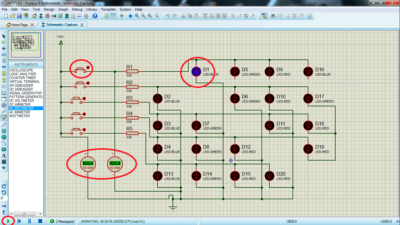
To apply this technique (charlieplexing), I simulated the probabilities to turn on the led lights on Proteus.
I wanted to understand the logics and probabilities to turn on the led lights on simulation.
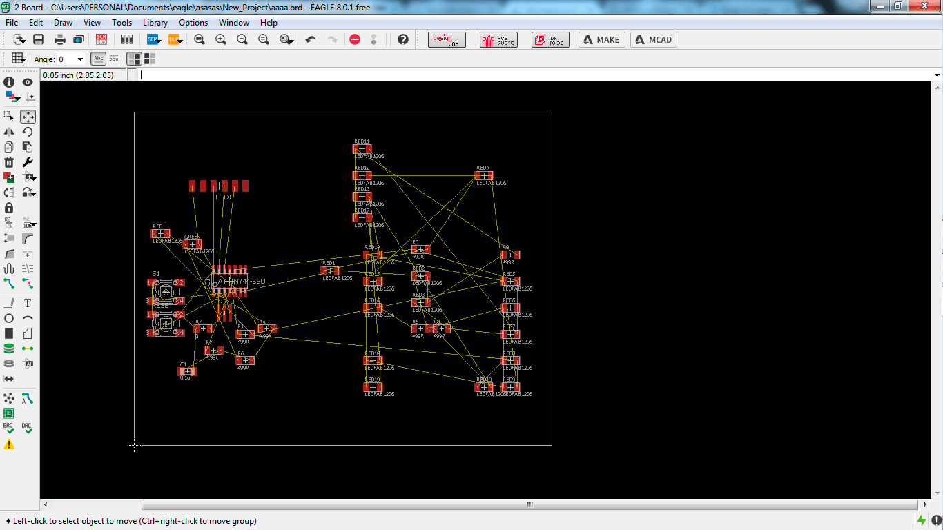
Second step is create the board
When you finish the schematic you have to create the board, to create the board you can find a button on the
schematic windows called "Generate/switch to board" then it opens the board window.
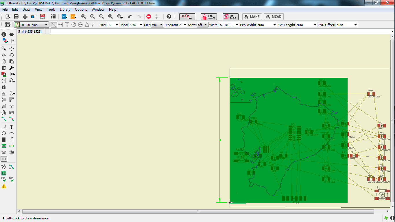
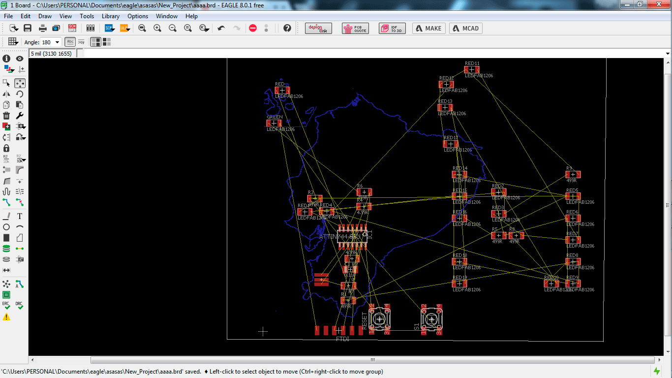
You can see all the components than you use in the schematic in your board window. then you have to move all the components.
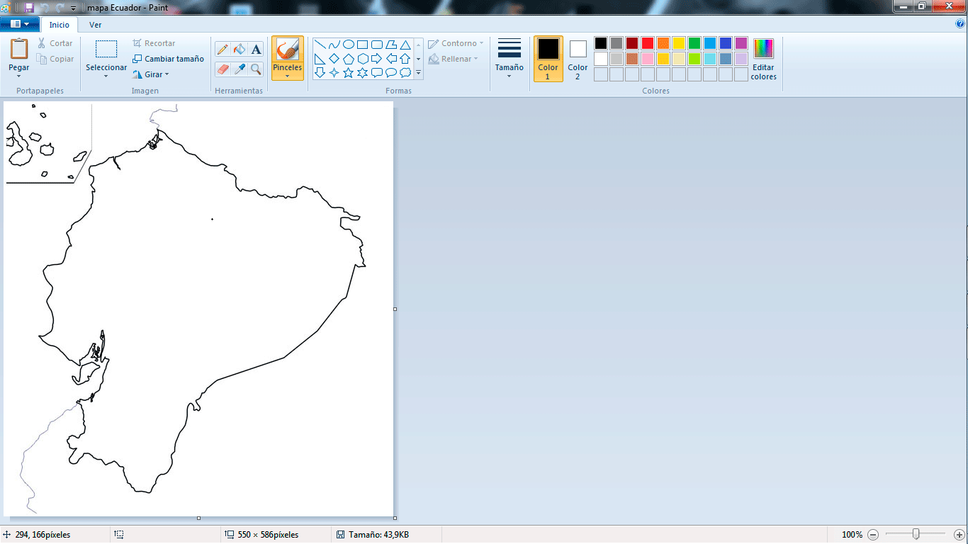
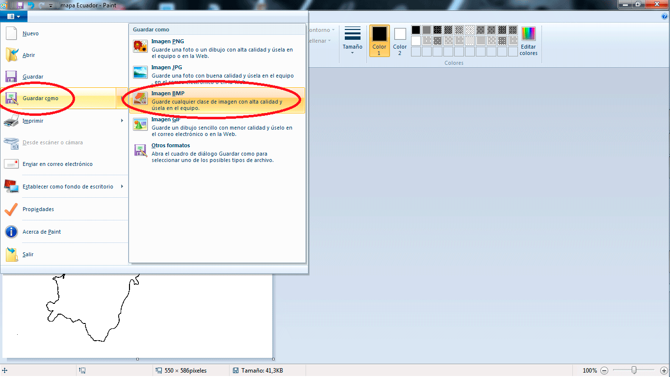
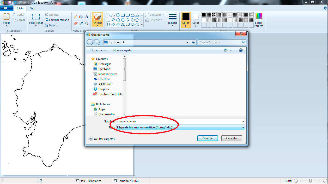
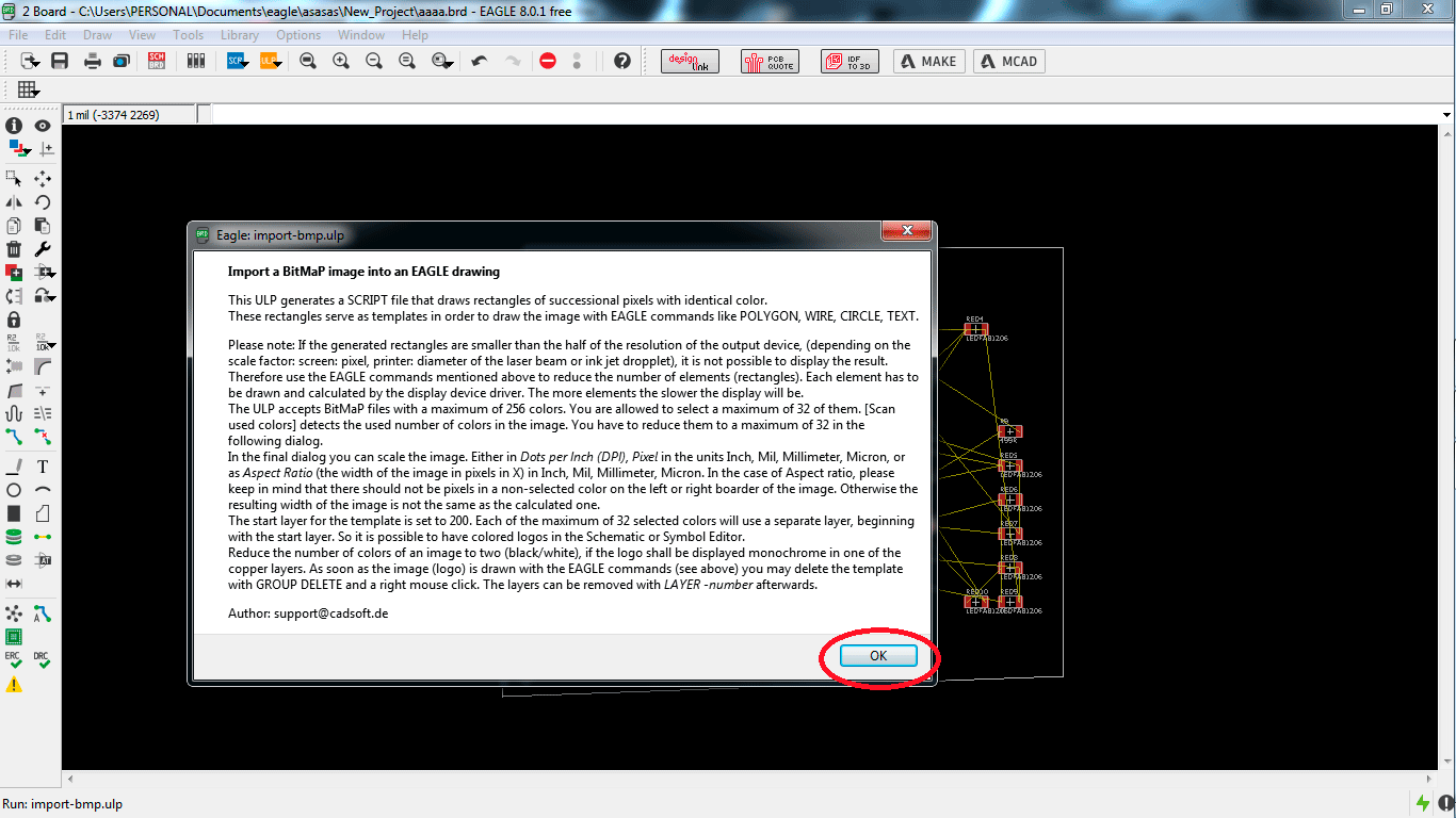
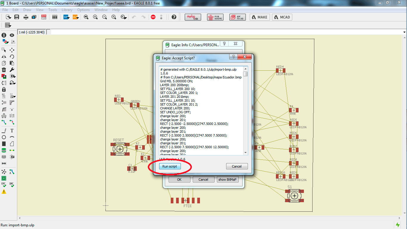
The idea is create a map with traces, to make it, I downloaded a image of Ecuador map, and I converted the format to " .bmp monochromatic ",
to change it I used "paint" software, I chose this format because Eagle PCB let me import bitmap files.
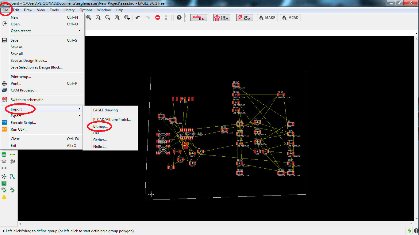
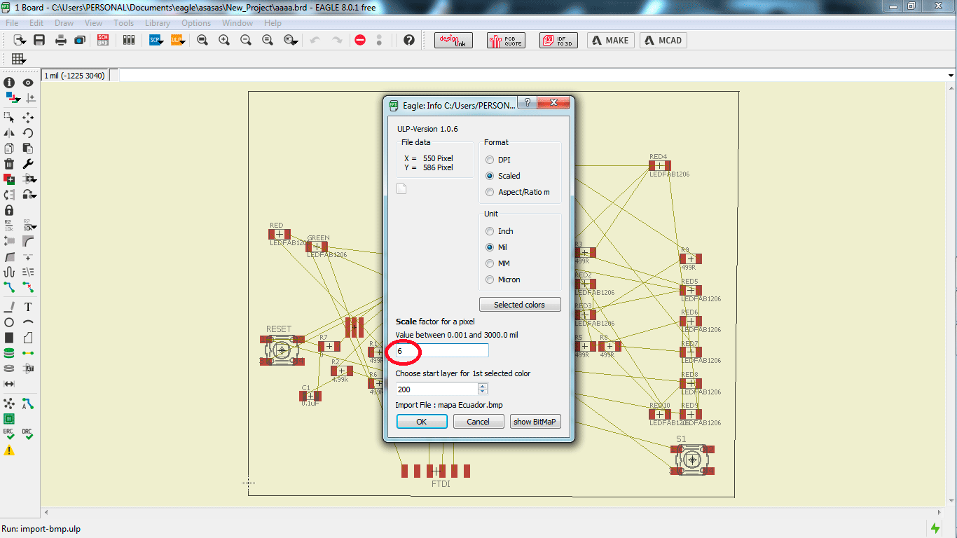
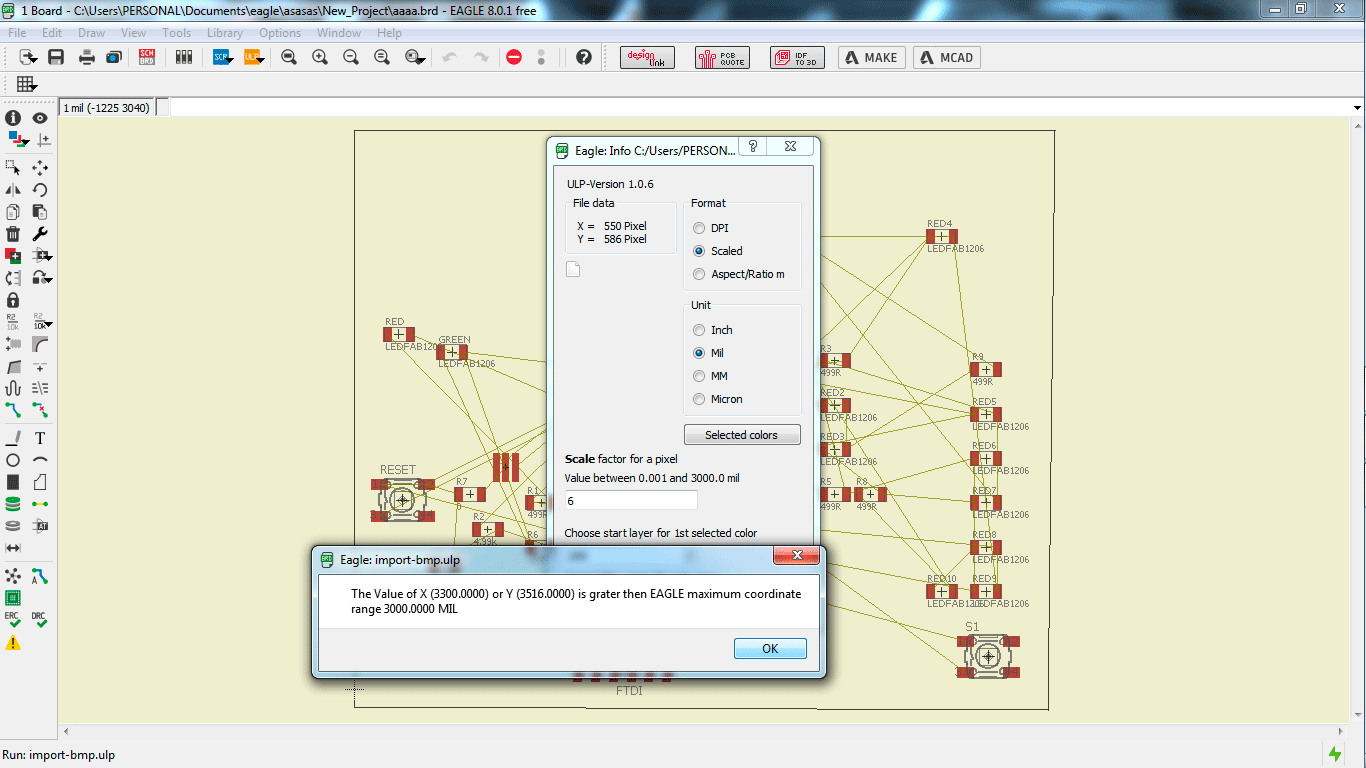
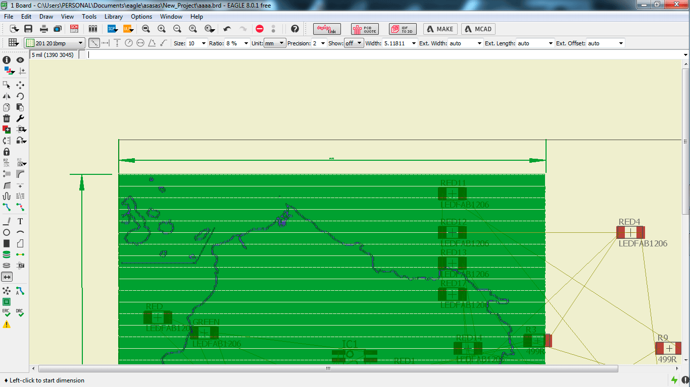
I imported the image to Eagle PCB, but I had a problem with the scale, the image is really small, I changed the properties in import
of 1 to 6 but finally the correctly was 5.
take in count the next steps to import an image to Eagle PCB.

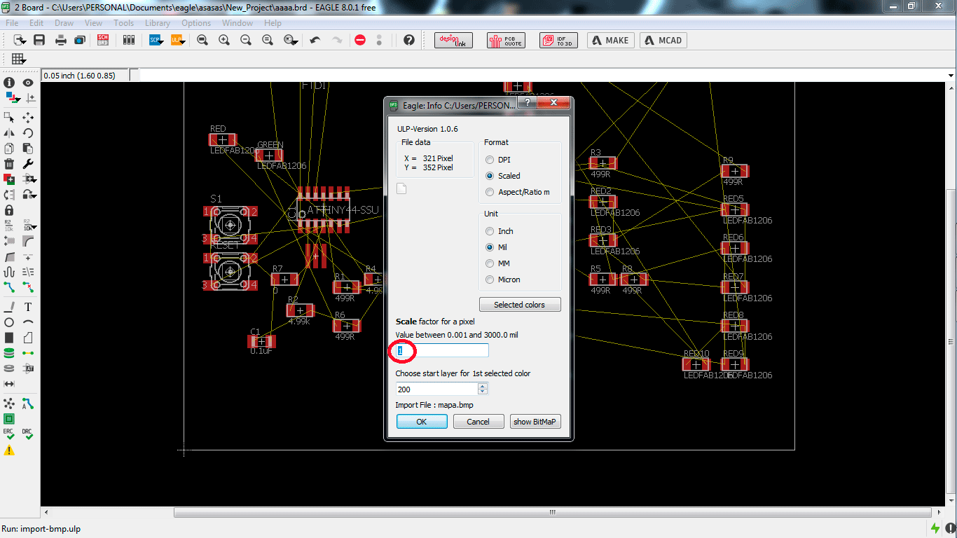
Changing the scale

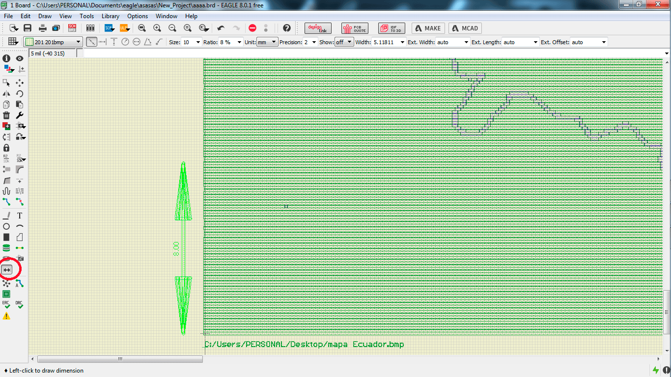
When you have your image ready, measure your size, if the size is ok, continue with the work, the size is really important take care.
To make a measure you can use the tool in the left down, you can see this in the image.

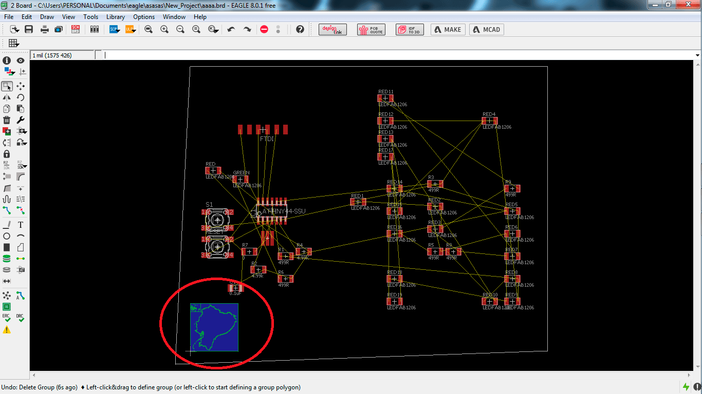
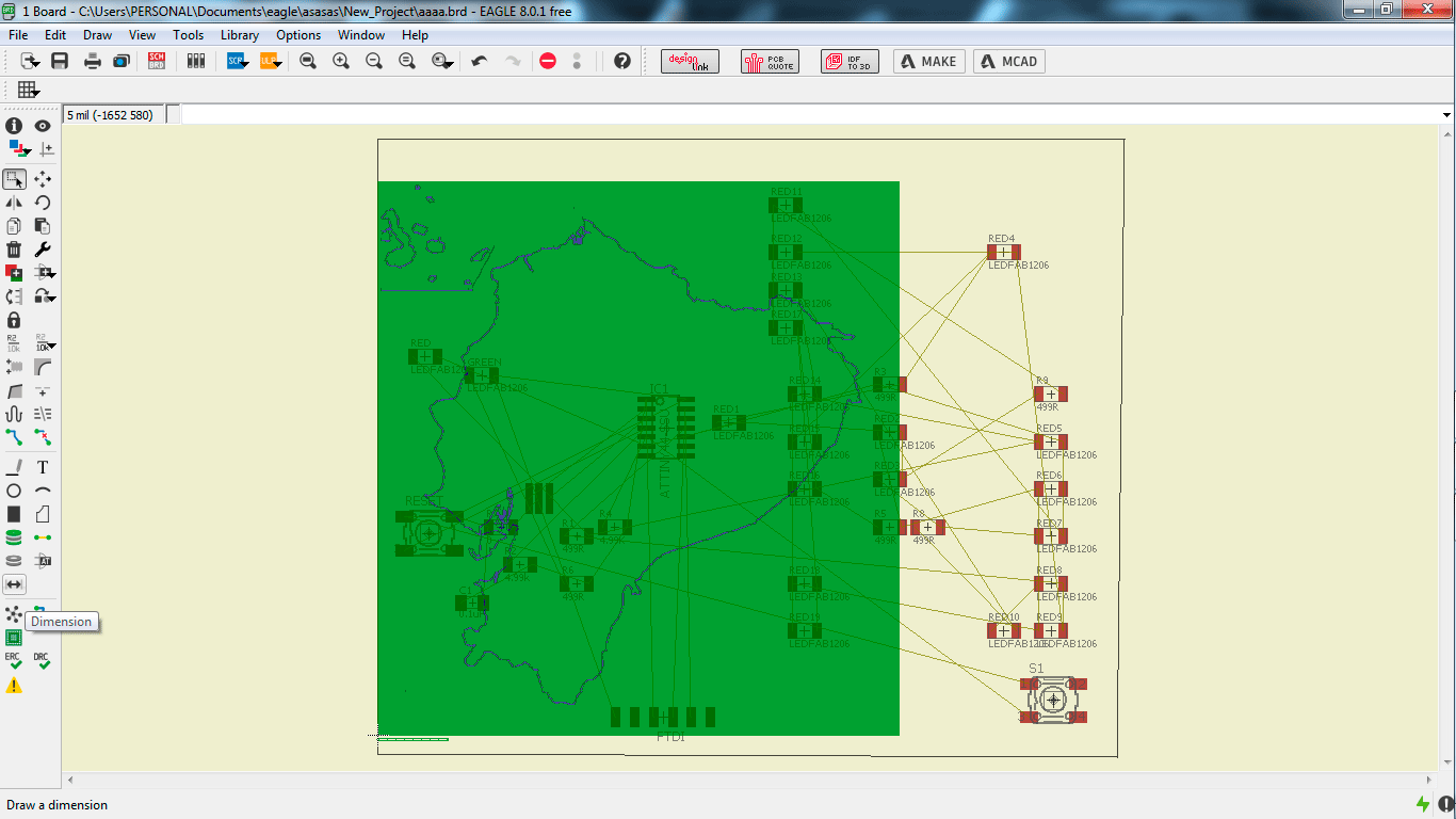
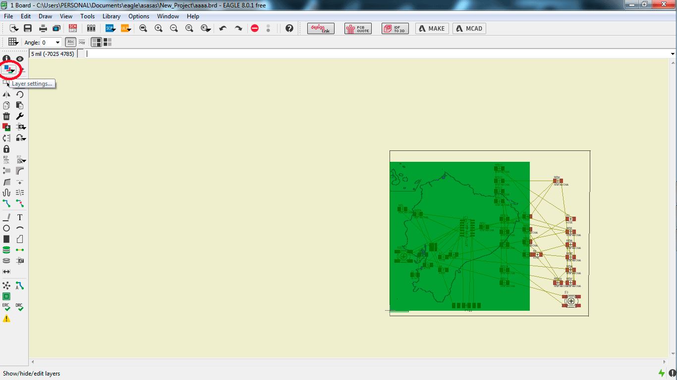
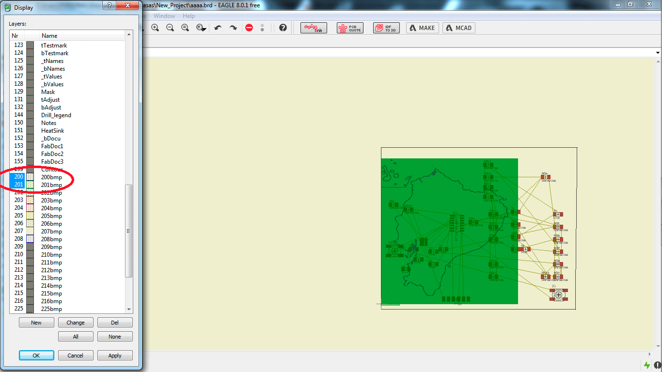
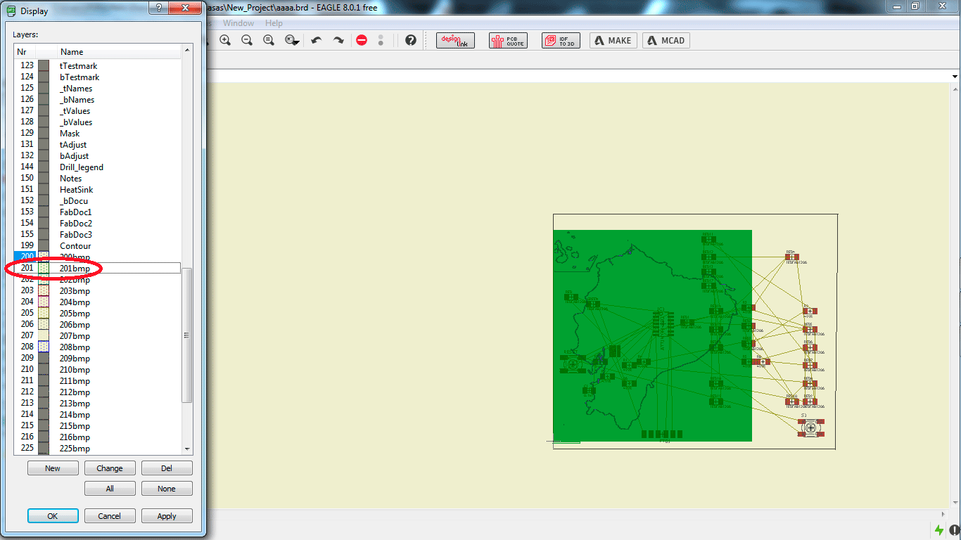
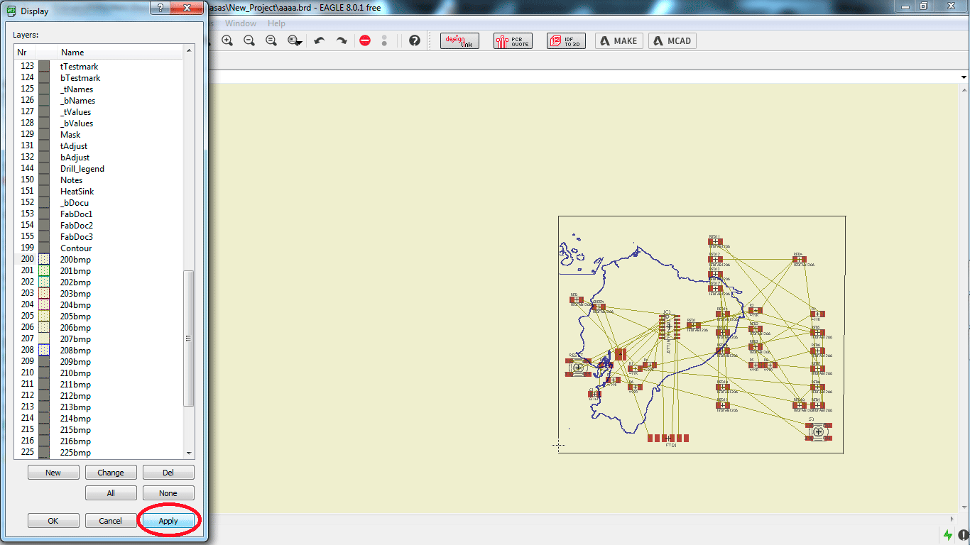
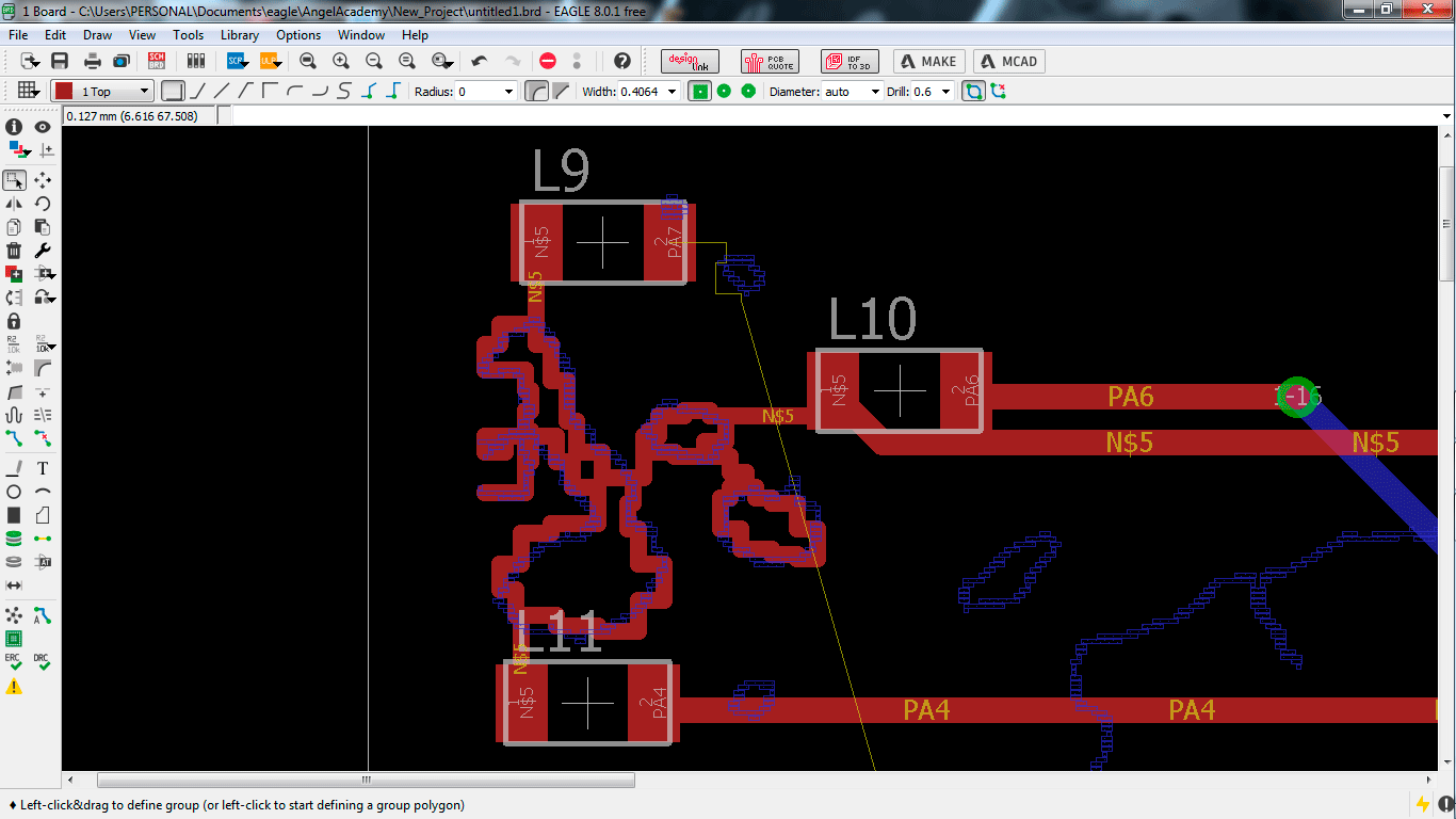
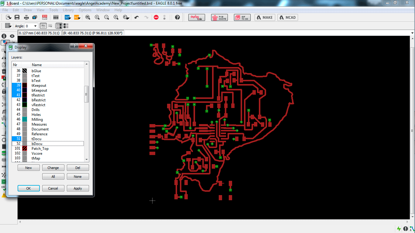
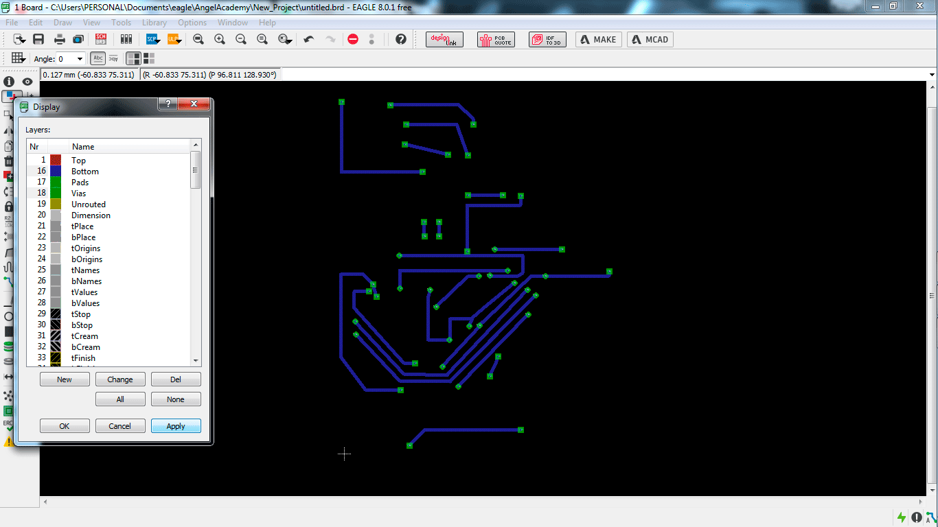
I uploaded the image, but it is a group of pixels, I need just the map, I need to erase the green layers, I chose the tool "layer settings" in the left.
lookingfor the option "201 bmp" and unmark.
I hid the green layer, if you do not hid the green layer you can not move the electronic components. I recommend to play with the layers to learn what they do.
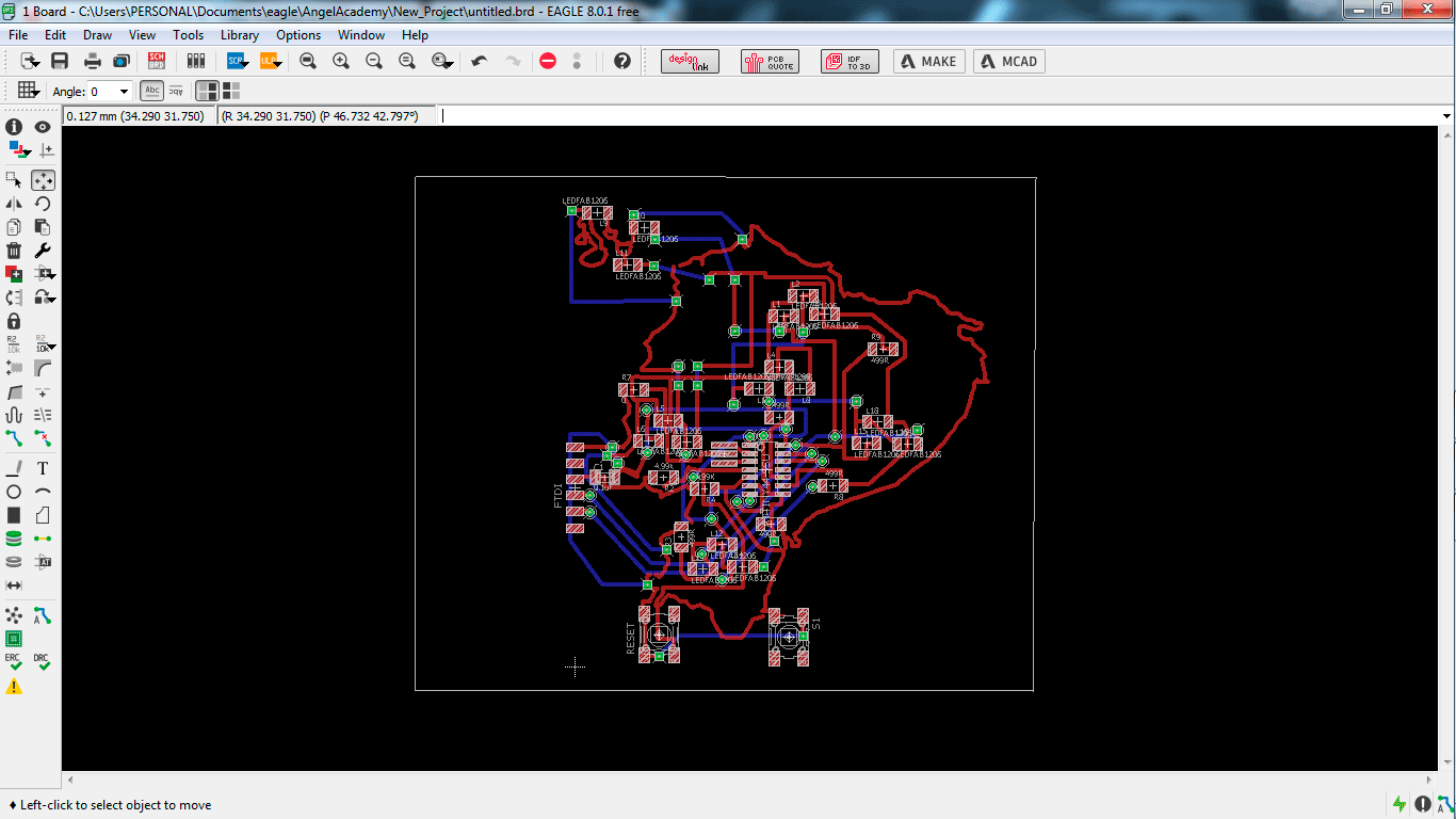
When the image is ready, I moved the electronic elements, you can move it where do you want. then I chose the tool "AutoRoute".
this tool opens a window called "AutoRoute mains setup", in this window I selected the option TOP and BOTTOM with /. it is to do the PCB in two faces.
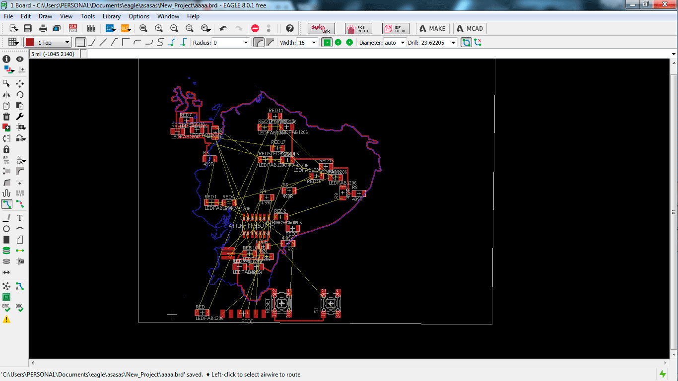

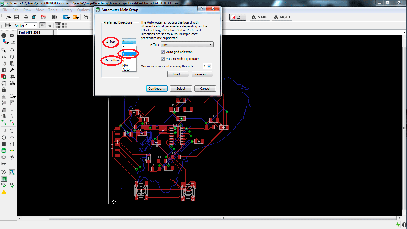
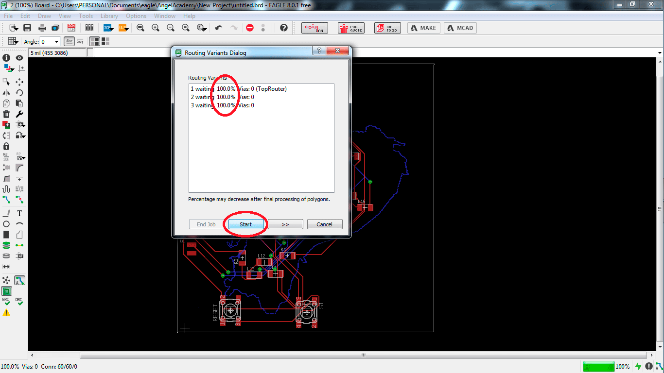
I chose the tool "AutoRoute" because I think it is fast but it was not the best option, I made it to have a reference and then I correct all the route, it is like a base to work.
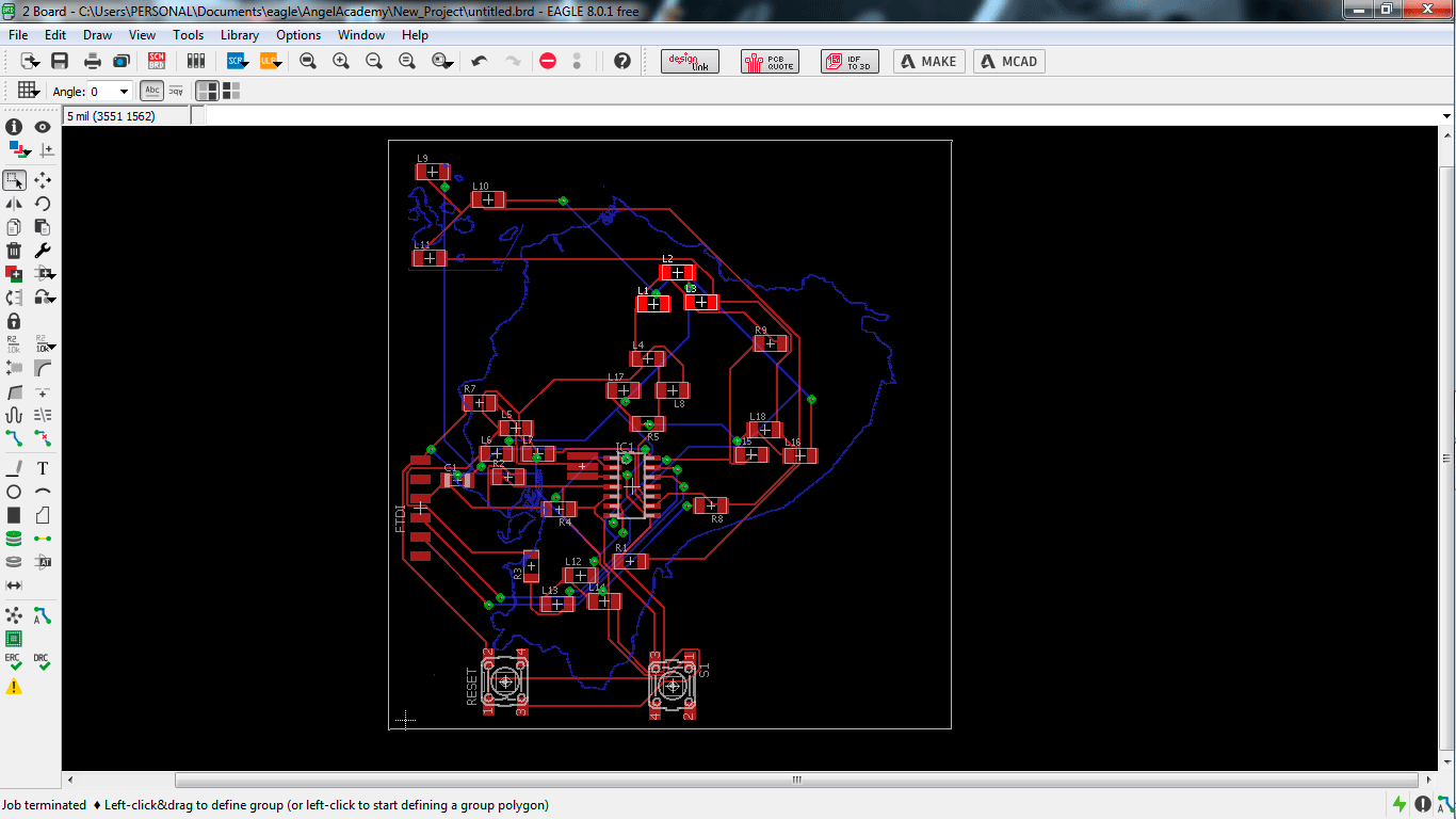
I made a process to get a better design.
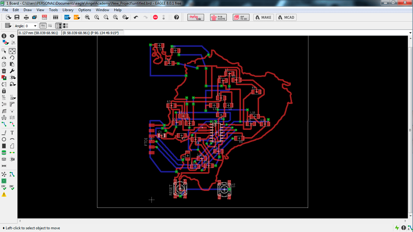
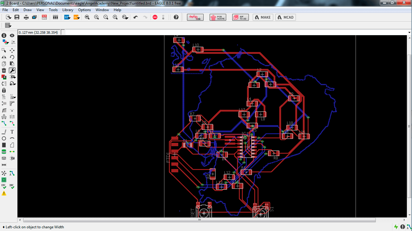
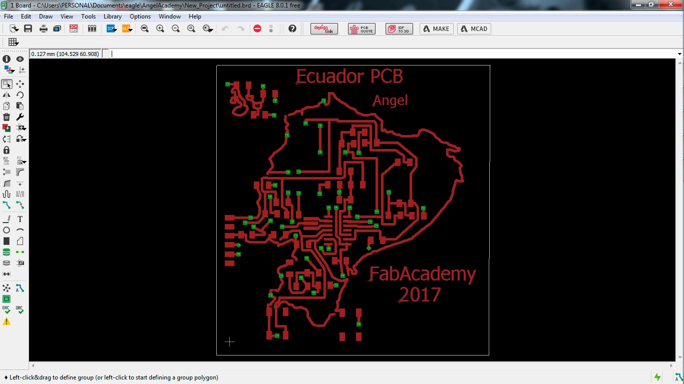
I moved some routes to get a better design, it is the final outcome, I think it was a great idea create this PCB, I am sure than some people has some good ideas like this.
A brain with led lights was mi first idea or a tree, but I feel so good to see the map of Ecuador. :)
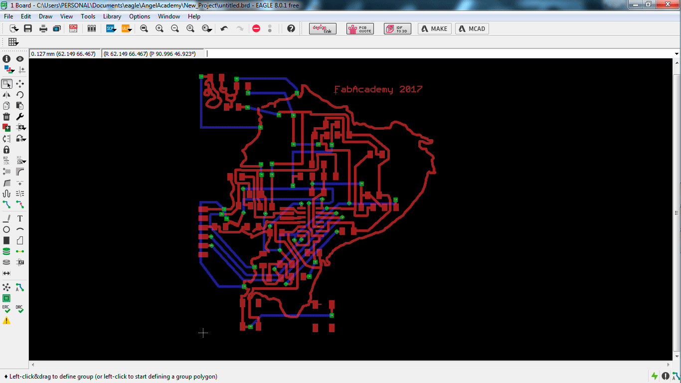
Finally, I decided to add text, I added the name of mi PCB, I decided to call it "Ecuador PCB" and my name "Angel" and finally "Fab Academy 2017".
4)Explained problems and how you fixed them, including how you worked with design rules for milling (DRC in EagleCad and KiCad)
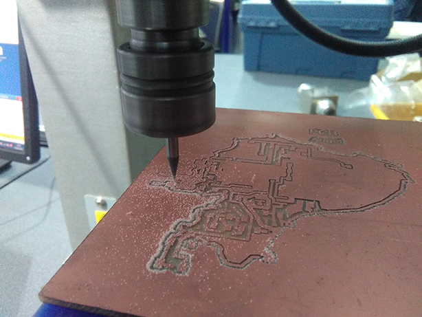
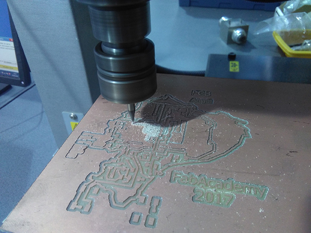
Third step is mechanize the PCB
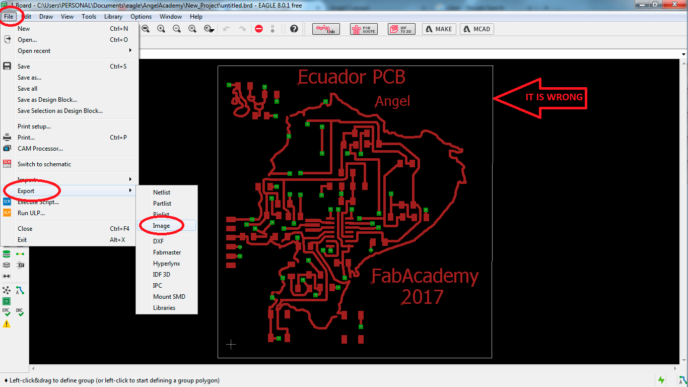
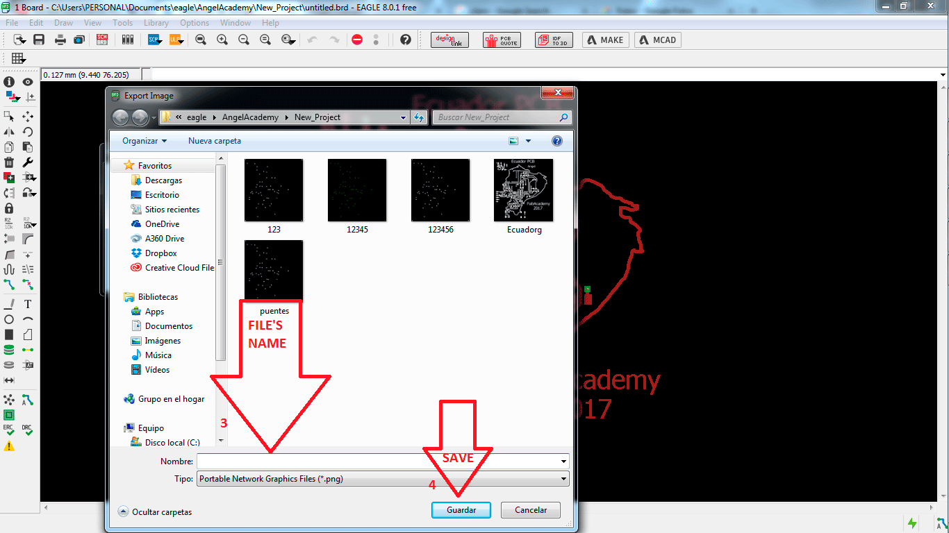
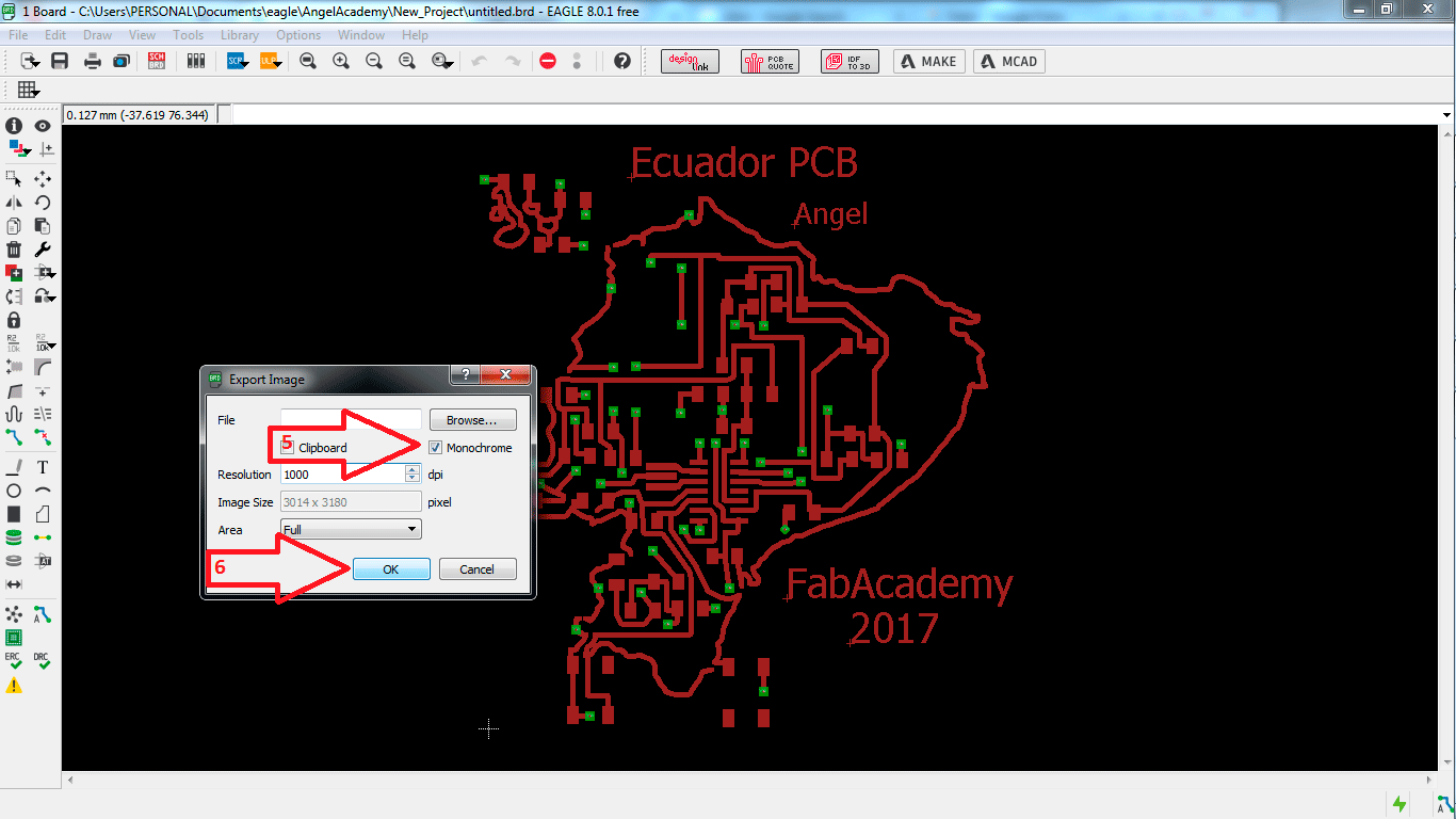
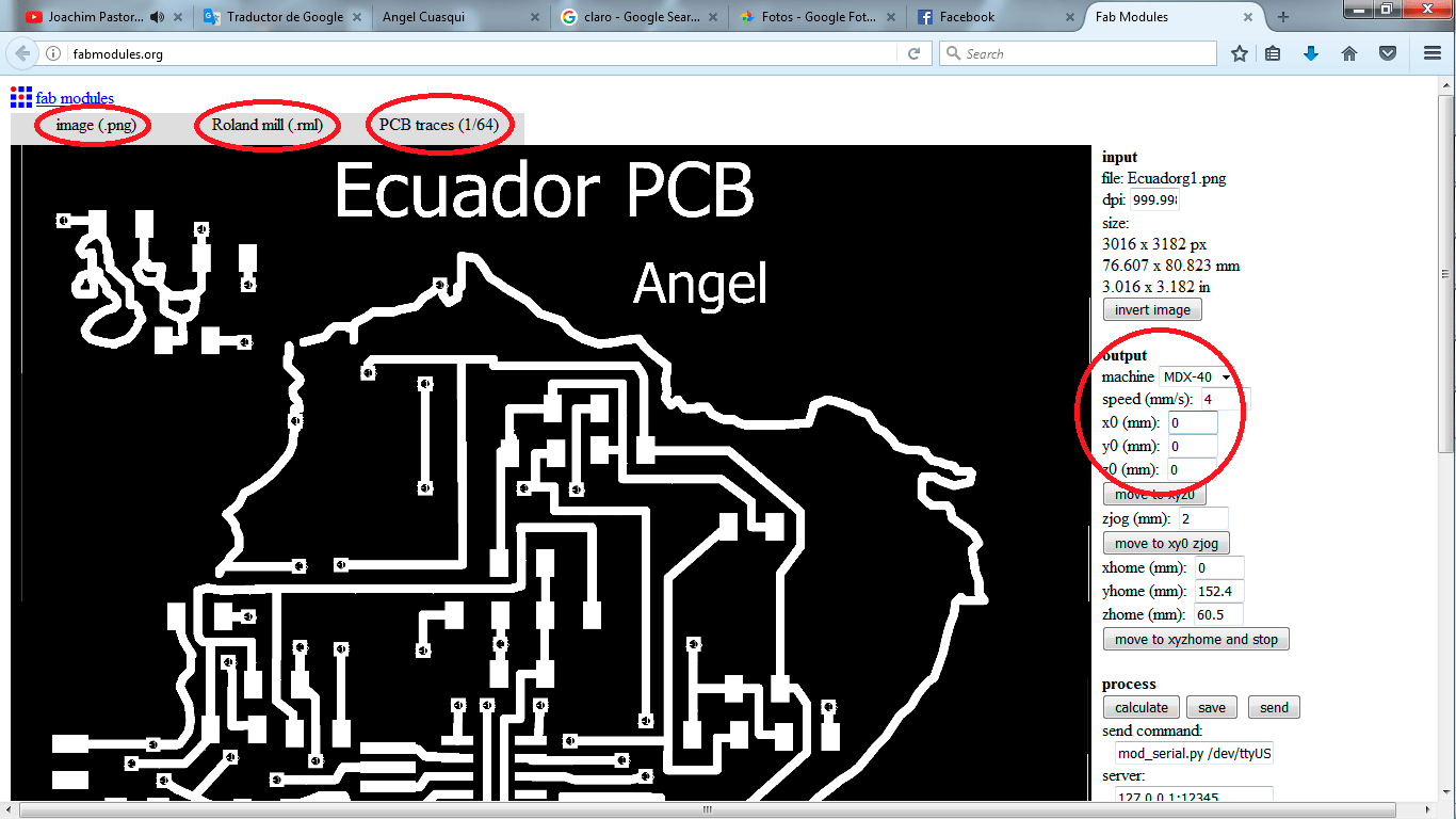
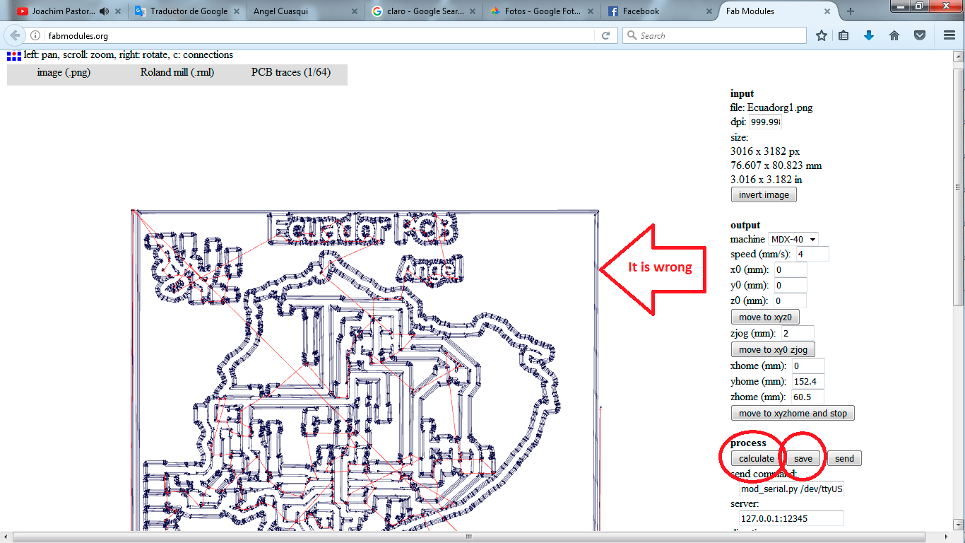
When you finish your design on eagle, you can export like an image, I export the image like .png file, because i need a .png file to upload on fabmodules.org. take care in the layers than you show.
my first fail is save the image to do traces with the exterior layer.
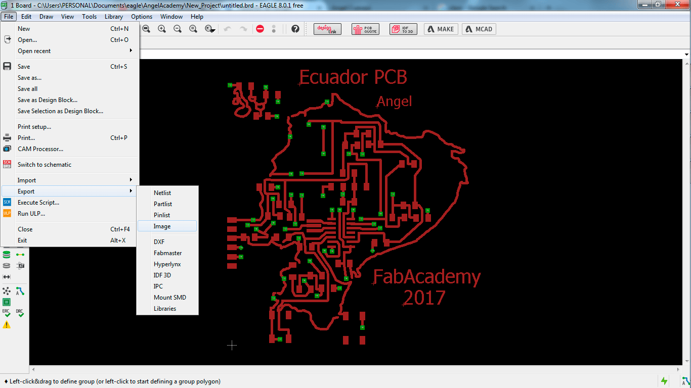
When you create the image to make traces , you do not have to show that layer because that layer is to cut no to trace. The second image is ok.
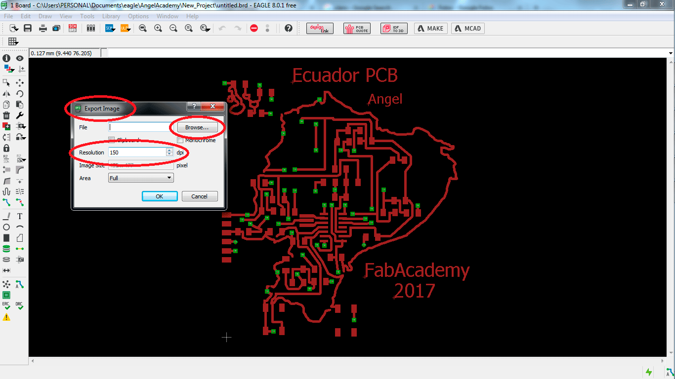
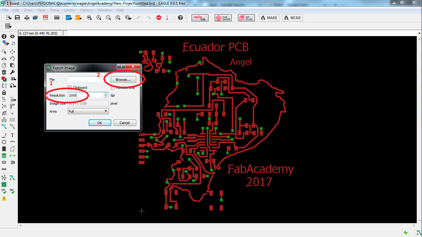
Then, press the option "export like an image", it opens a window to select the properties, select monochromatic and increase the resolution.
I increased the resolution to 1000 to get a good file to mechanize.
The steps to make it, is in the next image.
The image is ready, then we have to generate the tile in fabmodules.org, the cut deep is 0.25
All this files you can find in the finish of this page.
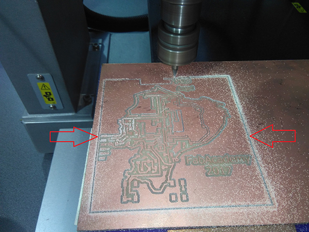
in the next images you can see my fail, the border is not ok because that is to cut and not to traces.
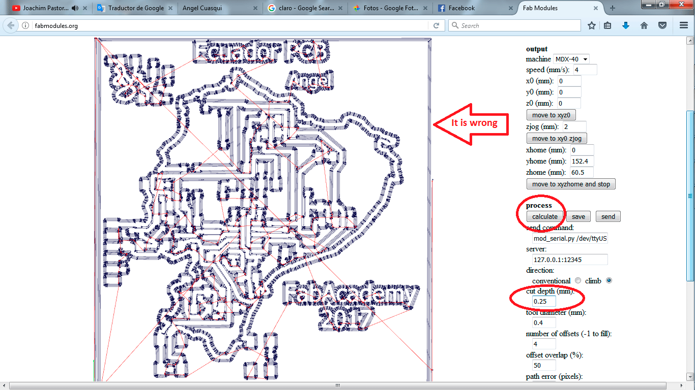
To made the PCB I used the Roland MDX540 machine, the cut deep is 0.25, the traces is 0.6mm. the machine finished the traces around 38 minutes.
You can see my fail, the border is bad because it is to cut not in this file, this file is to traces.
5)Included original design files (Eagle, KiCad, Inkscape, .cad - whatever)
Eagle board and schematic
png Files
bmp Files
4)Explained problems and how you fixed them, including how you worked with design rules for milling (DRC in EagleCad and KiCad)
Third step is mechanize the PCB
Eagle board and schematic
png Files
bmp Files