Assignment
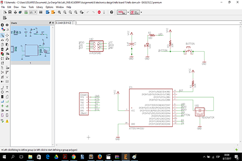
Redraw the echo hello-world board
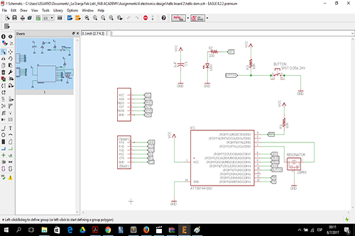
Add (at least) a button and LED (with current-limiting resistor)
Check the design rules, make it, and test it
Machines
Trotec Speedy 100
Soldering Heat Gun
Software
Adobe Illustrator CS6
Job Control
Materials
Antistatic table, Tweezers,
Solder Paste, 1/32 Milling Cutter,
Copper Board, Ferric Perchloride,
Solvent, Spray Paint
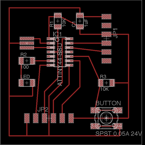
Electronic Components
1x 6-pin programing header
1x 6-pin line connector
1x Microcontroller ATTiny 44
1x FTDI header
1x Crystal Resonator 20 MHz
2x Resitor 10K
1x Ceramic capasitor 1uF
1x LED red
1x Button 0.05A 24V
1x Resitor 499 Ohm
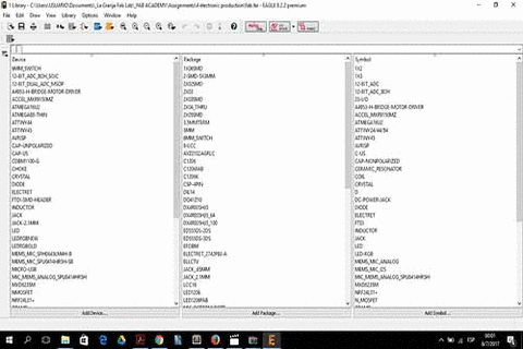
PCB Design and Schematic Software
EAGLE Autodesk
Eagle is a PCB CAD program for designing and laying out printed circuit board (PCB) designs
EAGLE works in two stages: Schematic capture and PCB design. In the first, the circuit connectivity is designed using the standard component symbols with which we are all familiar. In the second stage, the components are positioned on the printed circuit board and then traces between connected components are laid out.
Getting Started
1. Start Cadsoft EAGLE from the windows start menu (Start → Programs → EAGLE Layout Editor 5.x.x → EAGLE 5.x.x)
2. The first time that you run EAGLE, it will ask whether you would like to create a directory, click yes.
3. Expand the ‘Projects’ node of the tree on the left of the EAGLE menu.
4. Right click on the ‘eagle’ folder and select ‘New Project’. Name it ‘LPF’ (for low pass filter).
5. Right click on the LPF project folder (coloured in red) and select New → Schematic.
Creating the Schematic
1. Select File → Save and save the schematic
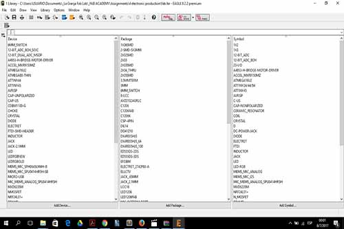
2. First of all, add all of the parts we will need (electronic components)
3. The schematic should look with the Basic part placement
4. Now for the connectivity! Select the ‘NET’ tool from the toolbox
5. Draw wires between all of the relevant terminals as per the original schematic.
6. Now we need to add the power and data ports
7. Complete the wiring
8. Finally, we will assign component values. Click on the ‘Value’ icon
9. It is a good idea to run an electrical rules check (ERC) to make sure you haven’t made any mistakes! Click the ‘Electrical Rule Check’ button and make sure there are no errors or warnings that you are not expecting
10. Make sure to save the schematic, and then choose File → Switch to board to begin creating theassociated PCB.
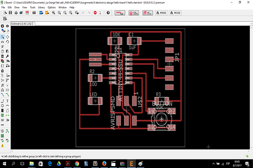
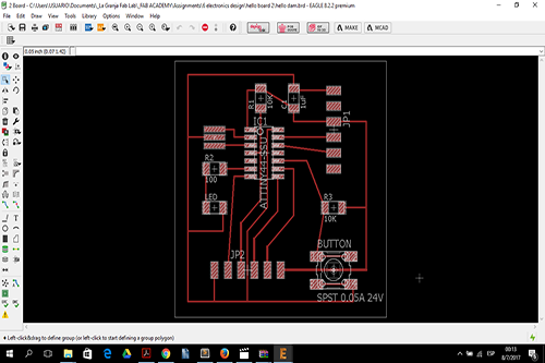
Creating the PCB
1. When asked if you would like to create the ‘LPF Schematic.brd’ file, click ‘Yes’.
2. You will now see a blank PCB board, along with the parts from your schematic in the lower left. The parts don’t look the same! These are the footprints associated with the components from the schematic. A footprint is the physical set of pin holes and copper areas that components of a particular side need to be soldered/clipped/connected to
3. We will begin by positioning the footprints on the board through a combination of rotation and movement. Mirroring a footprint is NOT allowed unless you are putting it on the opposite side of the board. There are more guidelines below (in the ‘tips’ section) but the important factors to consider here are:
a. Make the design compact.
b. Keep in mind that parts exist in 3 dimensions, and just because the footprints fit near each other, does not mean the parts will
4. Component footprints can be positioned using ‘Move’ and ‘Rotate’
5. Using the ‘Delete’ command, delete the existing board outline. Once the traces are laid down a new outline can be created to minimize the necessary surface area of the board. PCBs are priced proportionally to the number of holes in them and their total surface area, so saving space saves money!
6. With your layout completed, it is time to add the traces. Select the ‘Route’ tool
7. Make sure you are working on the side of the board you want. Layers (top or bottom normally) can be selected in the layer dropdown
8. To add traces to the board, first click on a connected pad, then click to lay the trace and finally click on the ending pad indicated by the dark yellow line.
9. In order to actually know what goes where after the board is manufactured, it is important to make sure that the component labels are visible on the silkscreen and won’t be on top of pads or drill holes or anything like that. In order to move the label of a part around, you have to first ‘Smash’ the part and then select and ‘Move’ the label
10. The final step is to arrive at the final board outline, which in this case will be a simple square. Select the ‘Line’ tool and make sure to select the ‘Dimension’ layer. Finally, draw the outline of the PCB board. Make sure to leave a bit of space around the edge of the board.
11. Use the ‘Design Rules Check’ to ensure there are no overlapping traces or other mechanical problems.