OBJECTIVES
Redraw the echo hello- word board Add (at least) a button and Led (with current-limiting resistor)
Redraw the echo hello- word board Add (at least) a button and Led (with current-limiting resistor)
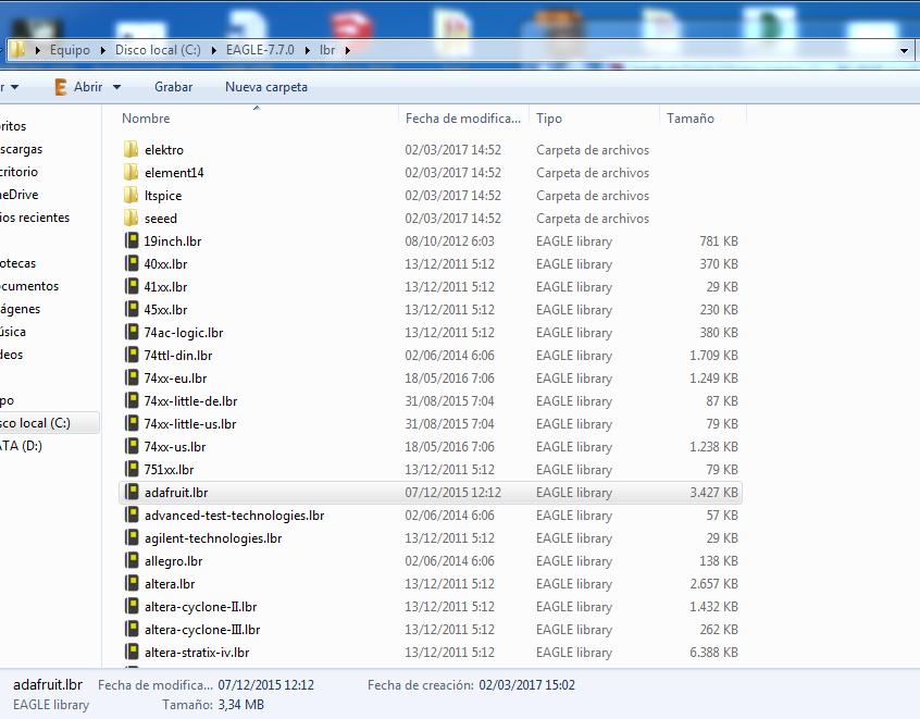
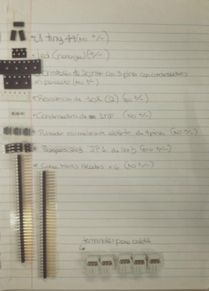
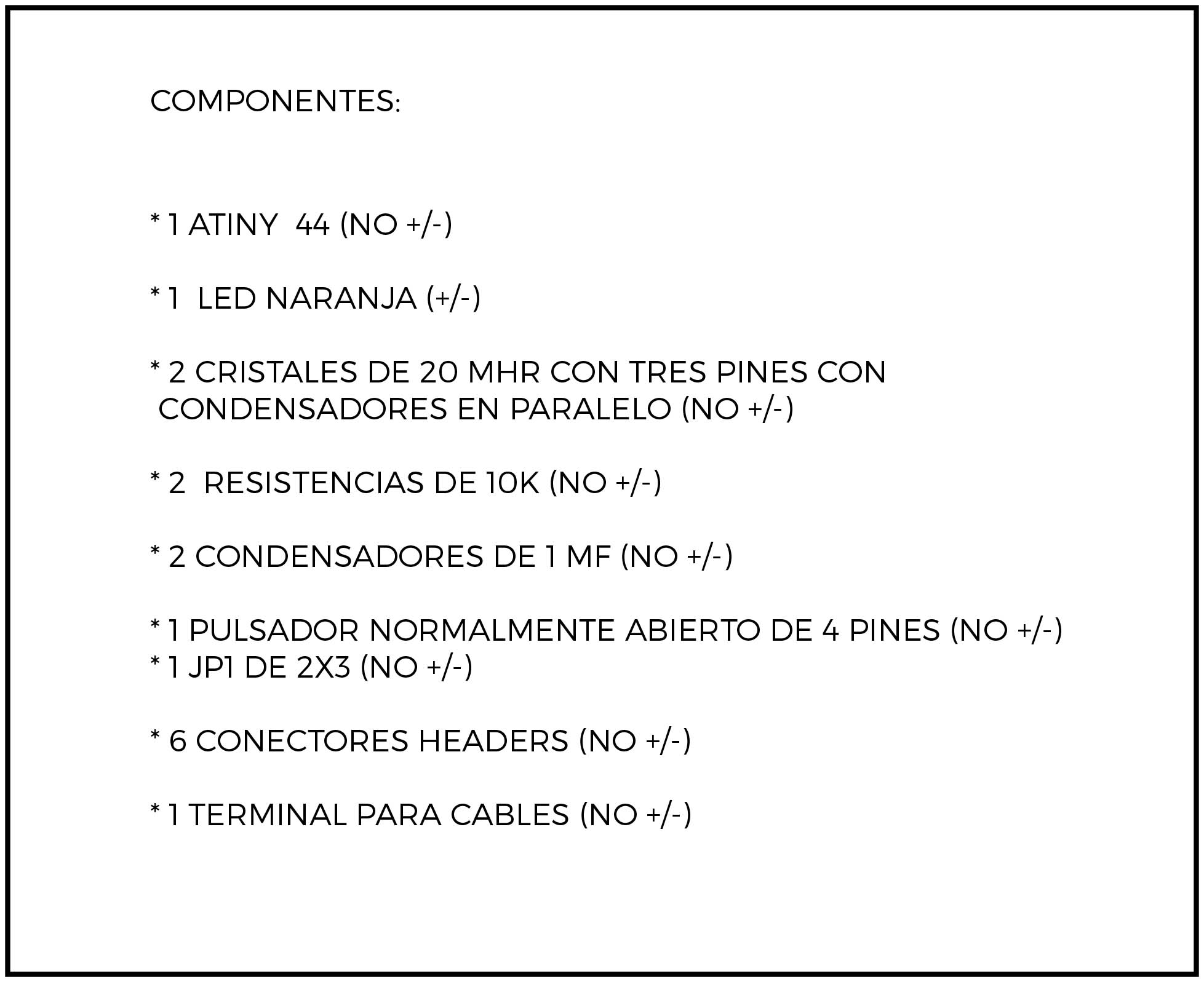
Electronics for me is very new, so I decided to “keep it as simple as possible” to be able to manage time and understand how it works. I used Eagle for this assignment, had to download the fab and Adafruit libraries (.lbr)
I After downloading the libraries, they must be safe in the C file in where the Eagle software is, in its own library file.
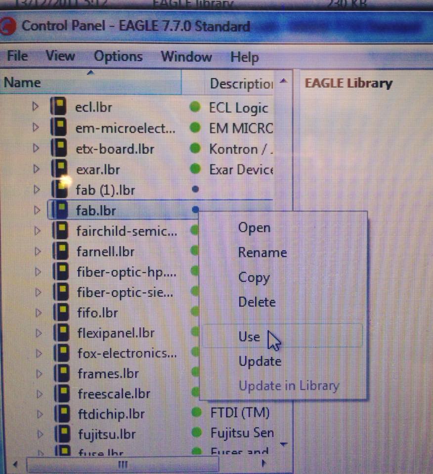
To activate the libraries, right click on them and then click on USE so the gray circle becomes Green.
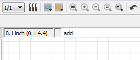
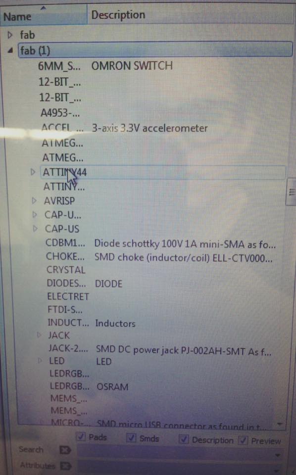
To work with Eagle, first one must open the Schematics, there you can load from the libraries all the components your circuit needed and design the structure. To find the components, write “add” on the top bar and click ENTER. There the downloaded libraries must appear and look for every component needed.
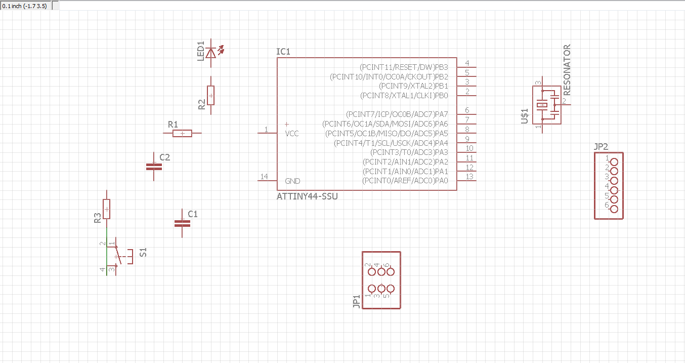
Once every component is there, use the Net tool to create the circuit.
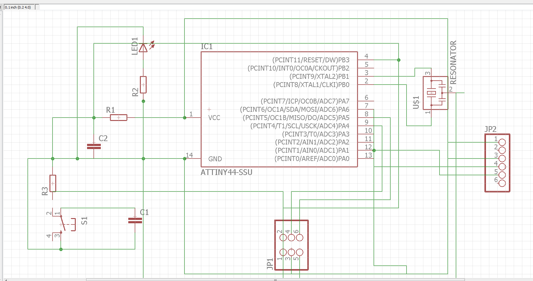
I did it twice, the first time was a little confusing with all the lines, then I learned that labels can be created for “GROUND” and “VCC” so you don´t get lost. When you ask the Eagle to create the board, it must recognize it. Second circuit design:
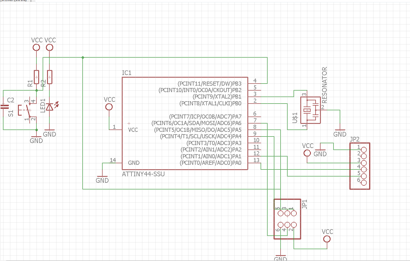
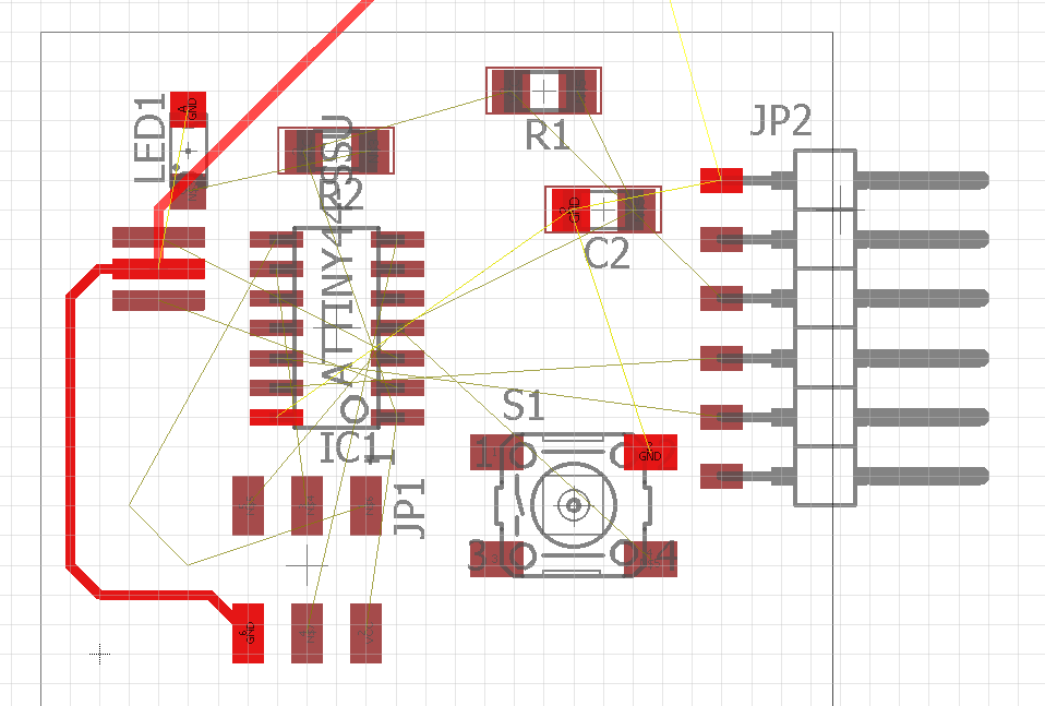
After revising that everything is connected where it should, generate the board from schematic. It would look like this picture :
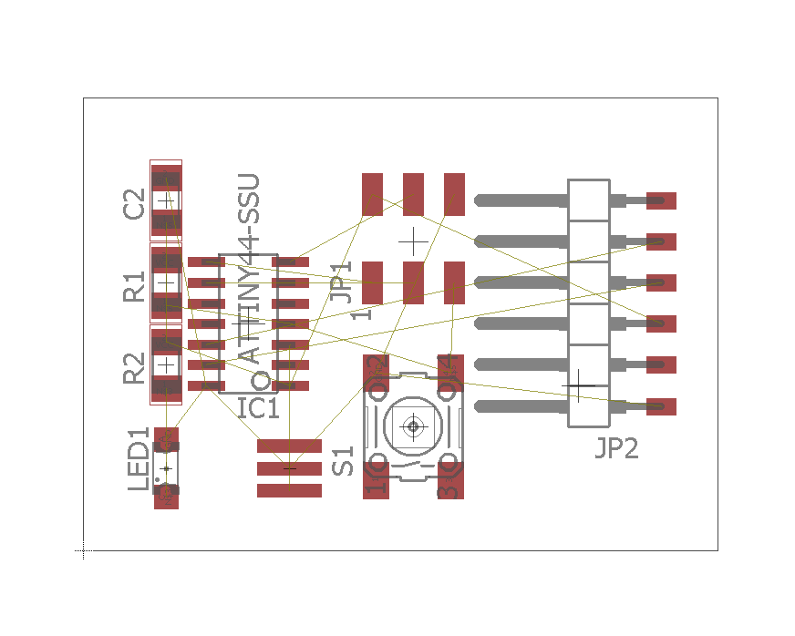
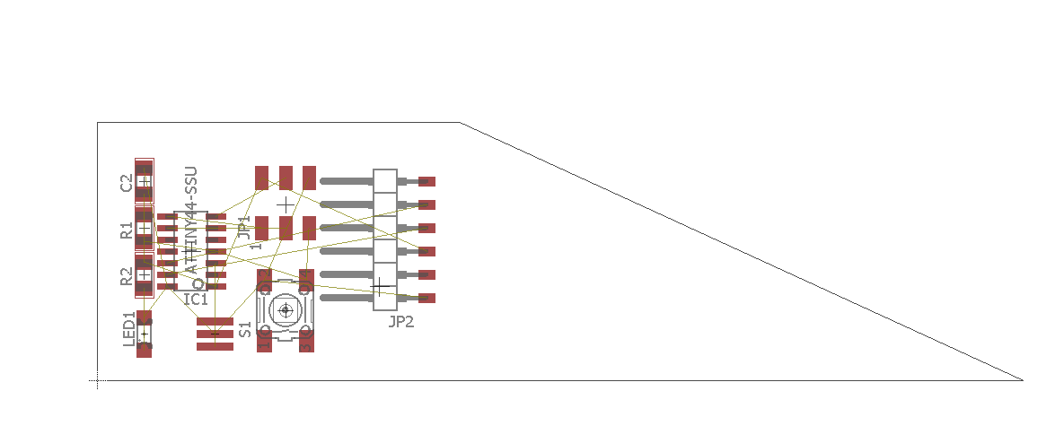
When yellow lines show where the components should be connected to the others. To move the card inside the working área, click GROUP, shadow the components, click CONTROL and RIGHT CLICK to move.
You can try the AUTO ROUTE tool to see what the computer generates and think it´s the best way to route.
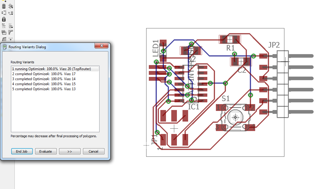
The red lines show the places where the route was done ok, but the blue ones show that the route can´t be made and that a cable must be use. So, delete the AUTO ROUTE and start routing manually. It´s important to know that you can turn the components with the RIGHT CLICK button, which make easier the routing process. This took me a while to find a way to create all the paths needed. When clicking on the route button and then clicking on the components, they´ll become bright red so you can see which must go together. Having in mind that the paths shouldn´t form a 90 degree angles or go over the components.
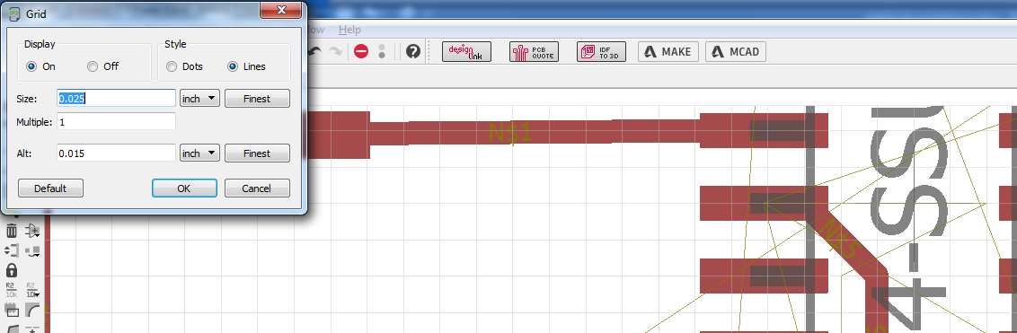
When wanting to erase a route use the RIP UP tool. There are some places where there is not enough space, for that go to GRID SIZE and ALT to move the routes better.
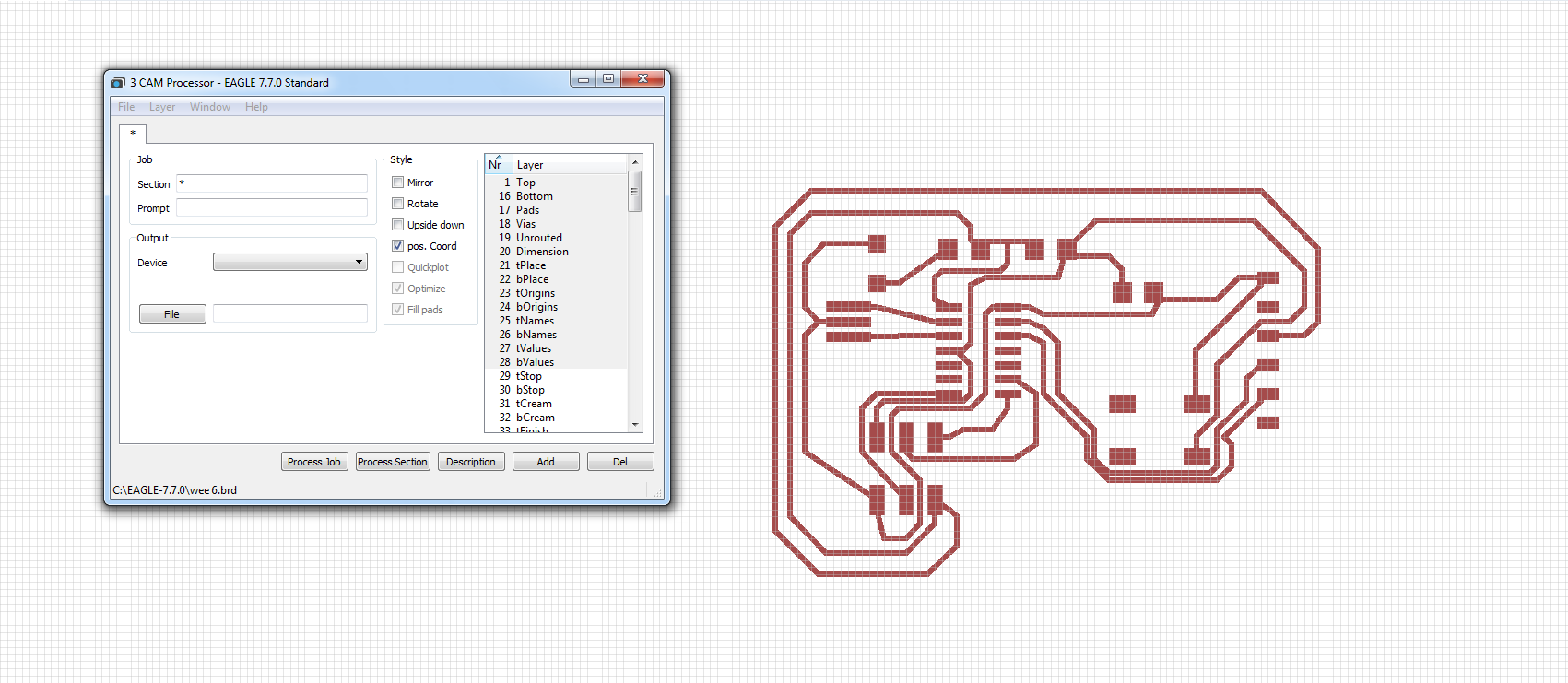
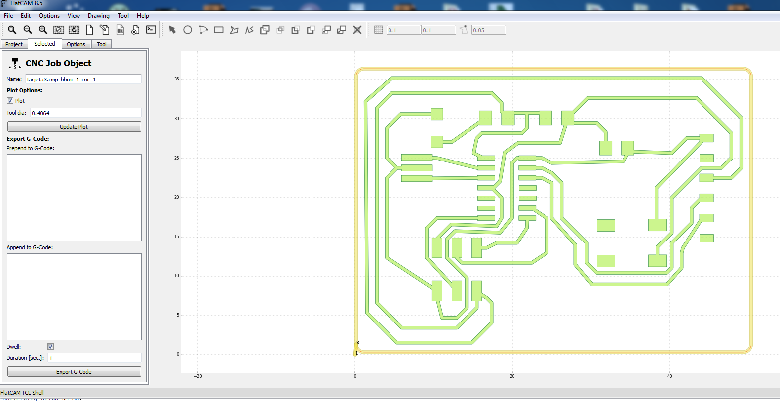
Go to CAM Processor and only select the top layer, which would only let the routing paths.
Go to FLAT CAM, to prepare the files for milling. Like in the ISP CARD assignment. The process can be seen in week four. But this time I had to go back and forth because when the milling file was generated, there were areas where the machine wouldn´t been able to reach.
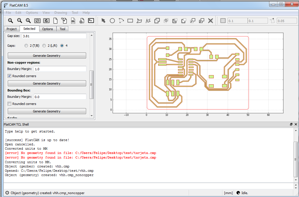
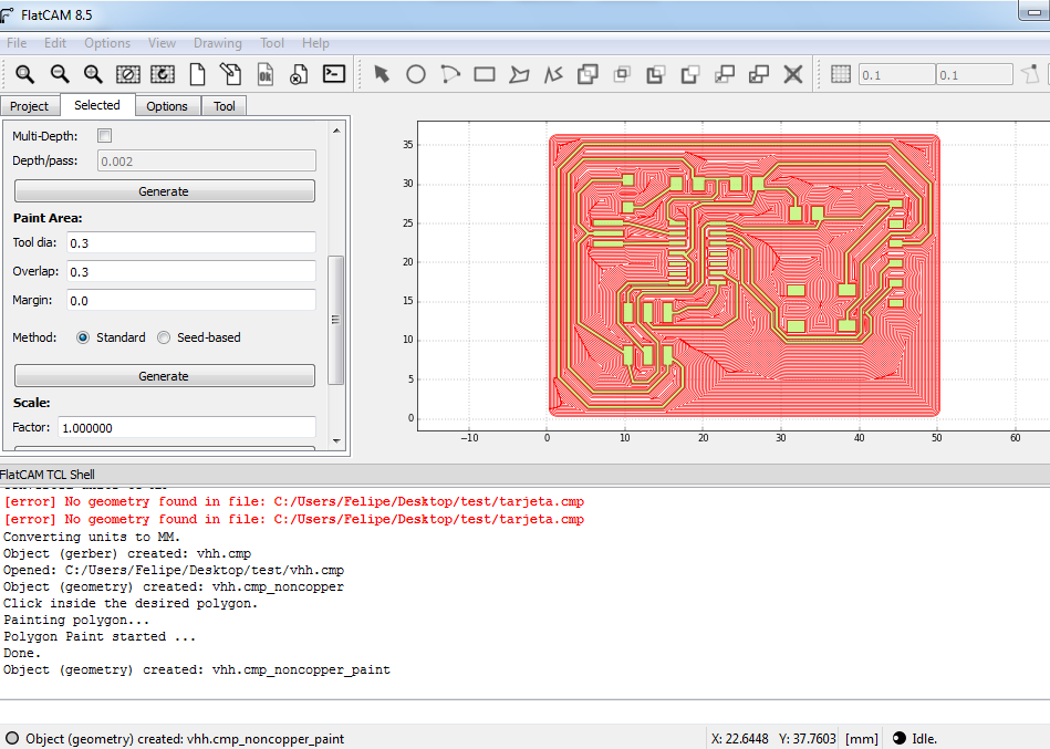
For that, I had to go back to the Eagle file and on the GRID button (top left) change the grid size, this would help to create smaller squares and the routing button would be able to move with more sensitivity. Allowing better detail when drawing the paths.
Whit that correction, I had to go back to Flat Cam to re-do the files for milling, including the border one for cutting.
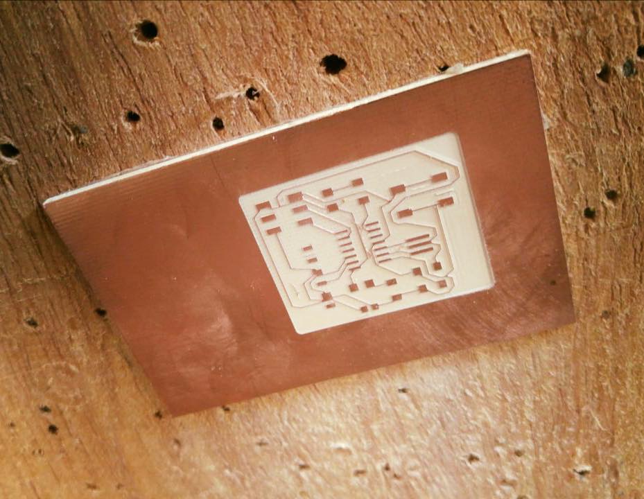
In the lab we have the MODELA PRO II MDX-540; in the preview milling assignment, we had some problems because the base wasn´t level.
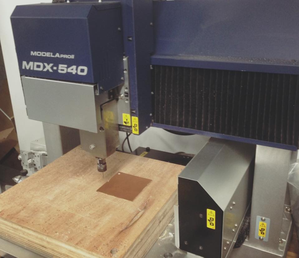
This time, I tried to mill where the level was better ,but even so, the corners of the card end up being a little lower and the drill didn´t do it´s job there.
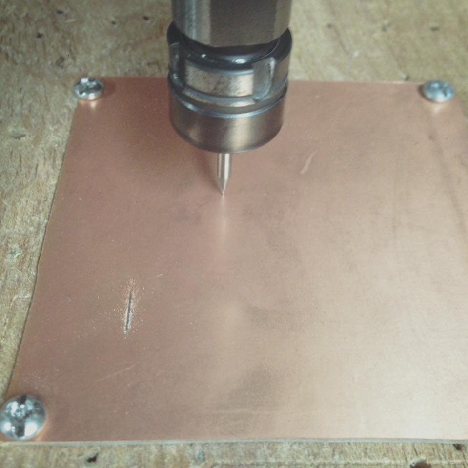
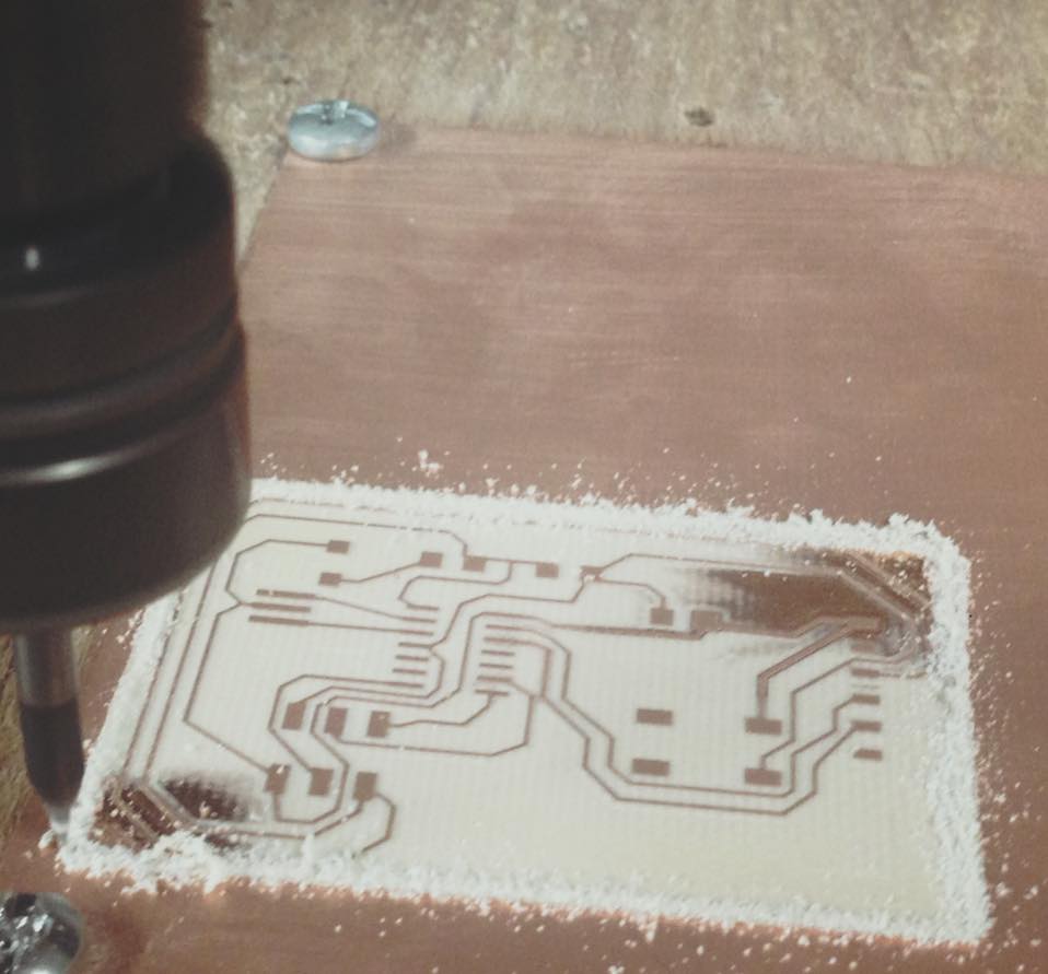
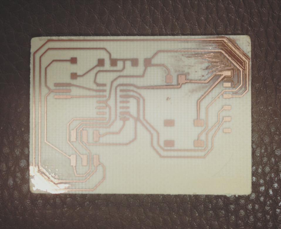
I used a cutter to try to finish “milling” while actually milling another card.
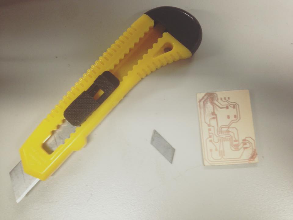
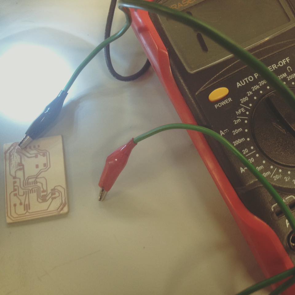
At the end, I finish with the cutter first, I checked the continuity of routes were ok.
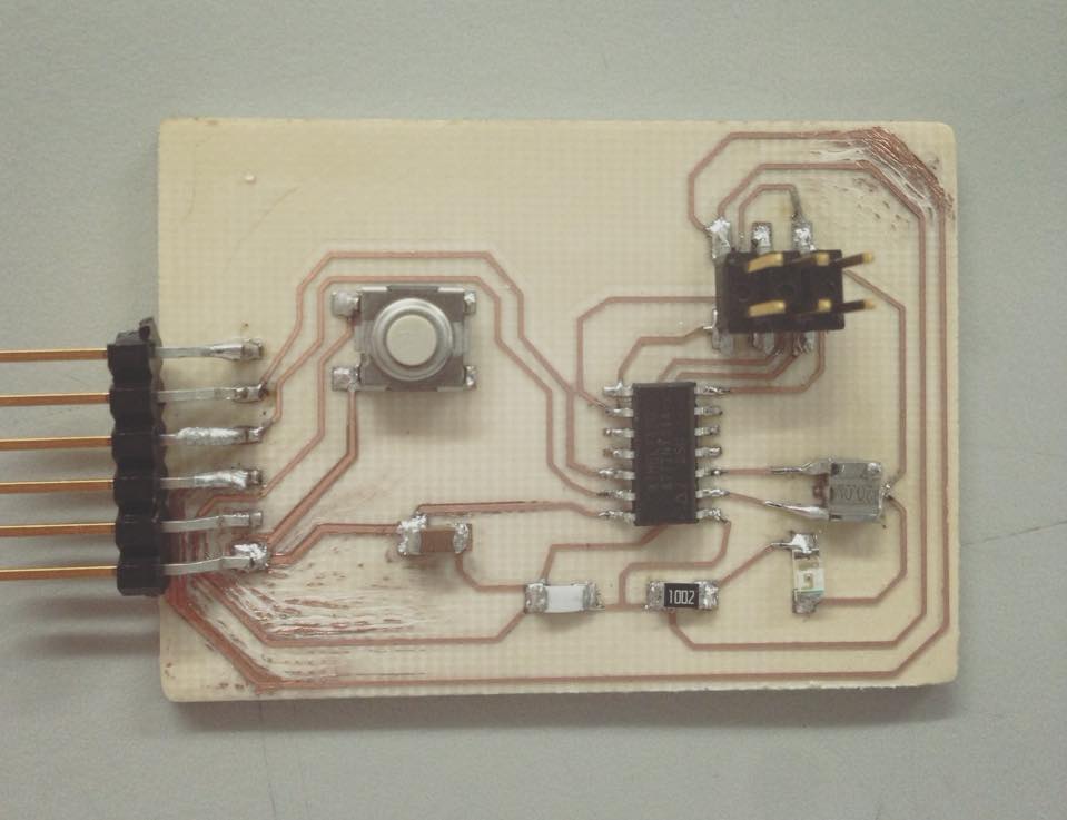
Then I started soldering the components
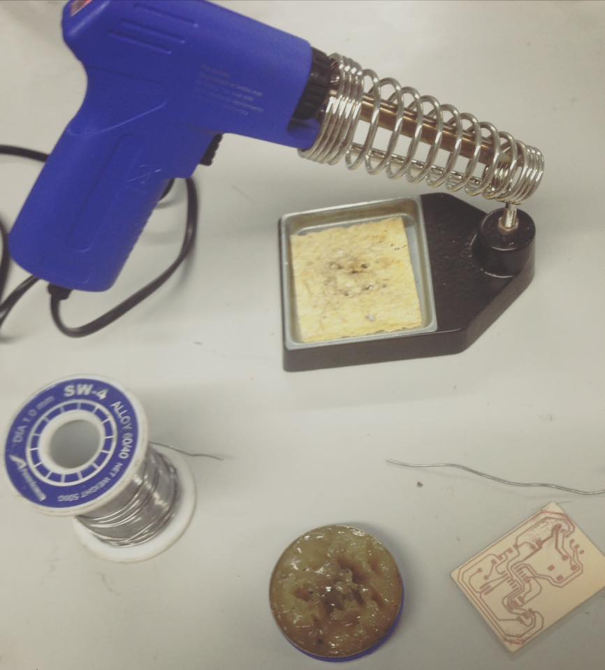
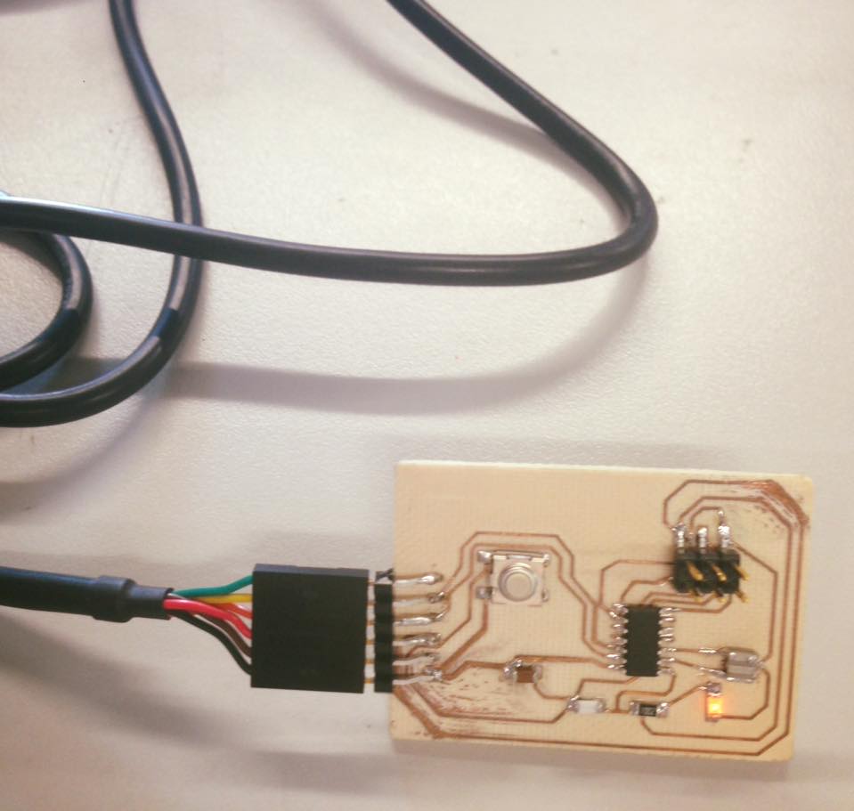
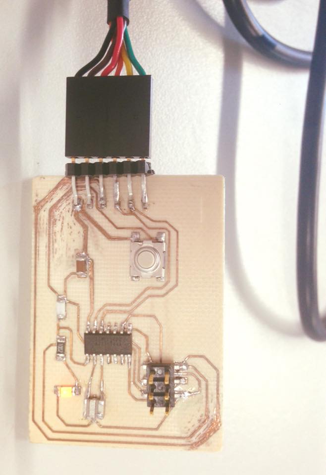
At the end, it looked like this with a button and an orange LED.