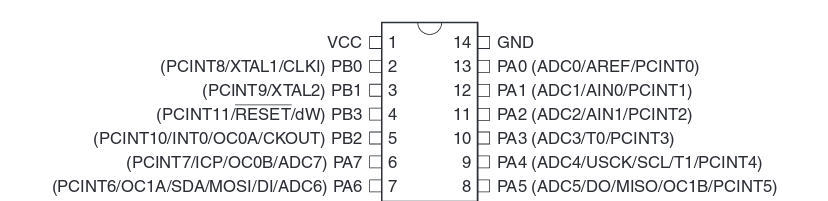
First I have learned is the pin out of the Attiny, which have 14 pins.
This image show the the pin out of the micro-controller
This week assignment is to read the attiny data sheet and programming my board to make anything that show that I have learned the programming.
For making this I have decided to use Attiny micro-controller.
Attiny is produced by Atmel company and have many advantages like
- Small size
- Fast and code efficient
- High integration
- 0.7 v operations.
This is the official page of Atmel for data sheet of attiny data sheet
First I have learned is the pin out of the Attiny, which have 14 pins.
This image show the the pin out of the micro-controller
So the micro-controller have one pin for the voltage VCC and one pin for ground GND so I can connect external power to it if I want to use it separately without using usb port of the computer, it also have 8 pins related to data register A DDRA and 4 pins related to data register B DDRB, PB3 can be used as the pin for reset.
One of the advantages of the Attiny is that it contain pull up resistor that I can use it.
For using a port I should write in the code the name of the register I will use then I activate the port then choose it as out put or input.
For example this is the code syntax to put PA5 as output
DDRA |= (1 << PA5);

  // set pa5 as output in DDRA
This code is to show how to put PB2 as input and activate the pull up resistor related to it.
``` DDRB &= ~(1 << PB2); // set PB2 as input in DDRB
PORTB = 0b00000100; // SET PULL UP RESISTOR IN PB3 ```
This a part of the code I will use in this assignment.
Now I have learned the first part in micro-controller which is how to choose the port and use it as input or output.
The second thing I learned was how to use the clock.
By learning the principles of how to use the clock I will activate something called sleep mode so I can make a power consumption of the micro-controller.
This image show the clock distribution in the micro-controller.
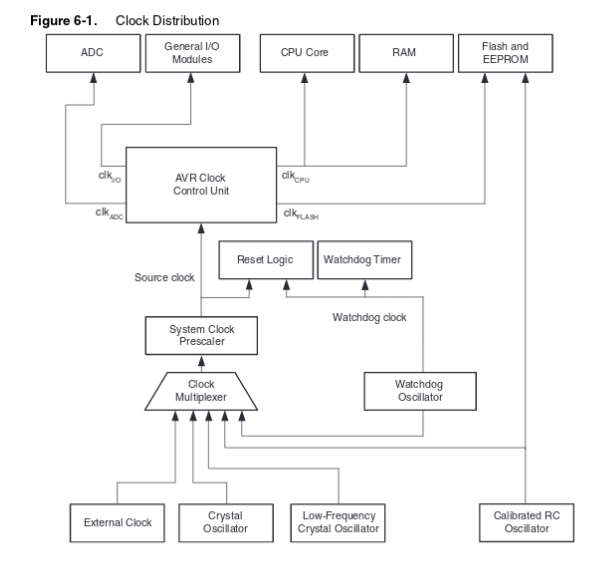
There are two types of clock internal clock and external clock.
what I will use is the external clock as I will put oscillator on all boards I will use as the intranal clock have an oscillator of 8 mhz and I decide to use 20 mhz.
The ATtiny24/44/84 system clock can be divided by setting the “CLKPR – Clock Prescale Regis- ter” . This feature can be used to decrease power consumption when the requirement for processing power is low.
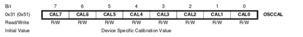
This is the code of activation.
CLKPR = (1 << CLKPCE); CLKPR = (0 << CLKPS3) | (0 << CLKPS2) |;
This for activating the clock on port PA3 and PA2.
Another thing I want to learn is analog to digital converter as my final project is an analog input.
Analog to digital converter in attiny have a lot of features like
- 10-bit Resolution - 1.0 LSB Integral Non-linearity - ± 2 LSB Absolute Accuracy - 13μs Conversion Time - 15 kSPS at Maximum Resolution - Eight Multiplexed Single Ended Input Channels - Twelve Differential Input Channels with Selectable Gain (1x, 20x)
- Temperature Sensor Input Channel - Optional Left Adjustment for ADC Result Readout - 0 - Vcc - ADC Input Voltage Range - 1.1V ADC Reference Voltage - Free Running or Single Conversion Mode
when I tried to use it I found that I can use it only on data register A.
This code shows how I activate it in port PA0 , PA1 ,PA2 , PA3 and PA4
ADMUX =  (0 << REFS1) | (0 << REFS0) // VCC ref
   | (0 << MUX5) | (1 << MUX4) | (1 << MUX3) | (1 << MUX2) | (1 << MUX1) | (1 << MUX0); // ADC0 PA0
 ADCSRA = (1 << ADEN) // enable
     | (1 << ADPS2) | (1 << ADPS1) | (1 << ADPS0); // prescaler /128
This a small part I have learned in micro-controller but I will continue in learning it.
I want to learn how to use interrupts at first and then laern how to use timers.
One question of questions I have why I should connect component need to analog to digital converter in register A only?
I decided to program the board I made in week Electronic design assignment
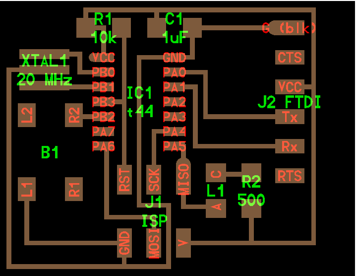
This board contain LED and push button so I decided to program it.
The goal of programming the board is that by pressing the push button it turns the LED off.
For programming the board I will use the c language.
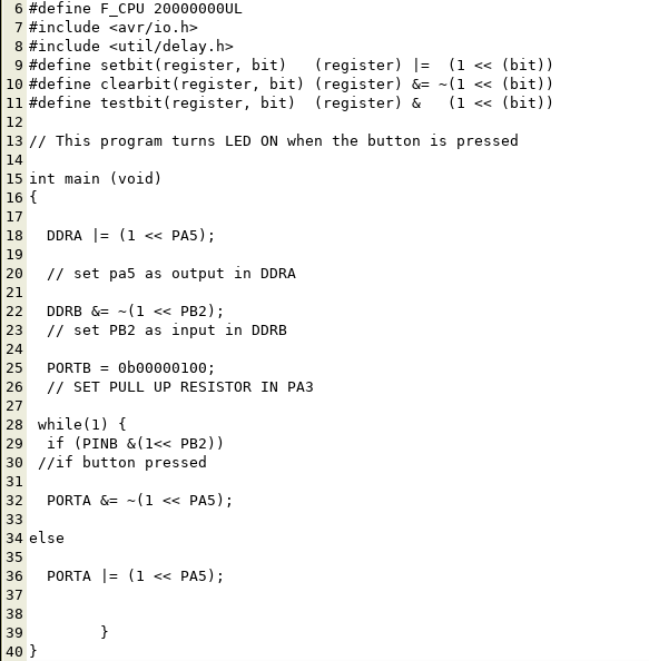
#include<util/delay.h#include<avr/io.hDDRA |= (1 << PA5);DDRB &= ~(1 << PB2);PORTB = 0b00000100;while(1) {
if (PINB &(1<< PB2))
//if button pressed
PORTA &= ~(1 << PA5);
else
PORTA |= (1 << PA5);
}Now I finished the code then I should have the make file I download neil make file and modify on it.
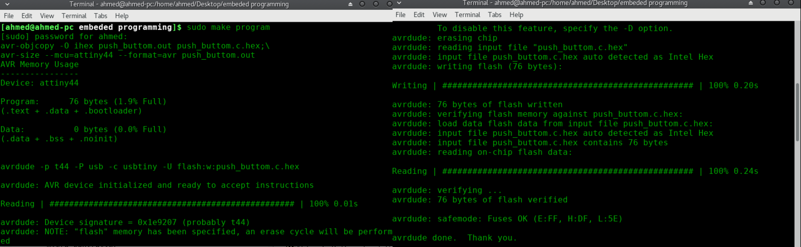
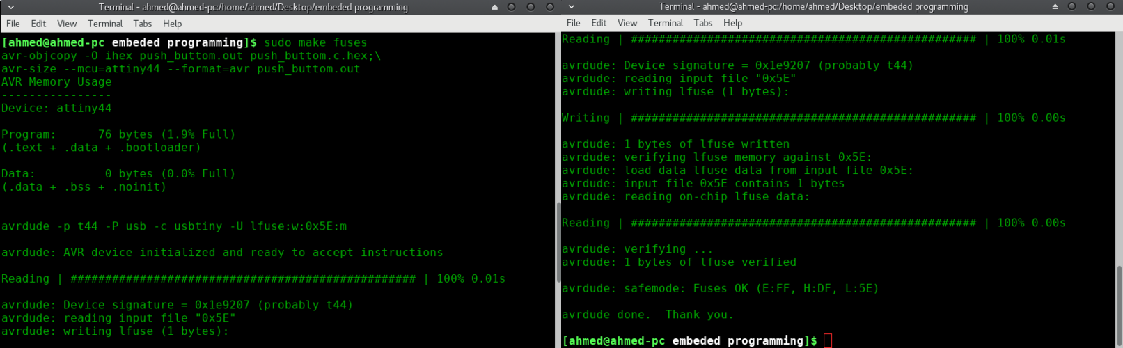
After I had the the code file in C and make file I opened the terminal and start wrote sudo make program This to generate the hex file to upload it on the board and then for burn the fuses I write command sudo make fuses .
This image show that I successful upload the program to the board
This image show that I successful burn the fuses and the board ready for working
Now I finish the program and uploaded it to the board and the board working.
I use programming in c as I have full knowledge about arduino and I want to learn new things.
This video show the board working when I upload the code on it.