6. Electronic Design
Index
- Assignment
- Introduction
- KiCAD
- Eagle
- Milling the board
- Soldering
- Programming the board
- Testing the board
- Problems faced
- Summary
A. Assignment
- Redraw the echo hello-world board, add (at least) a button and LED (with current-limiting resistor), check the design rules, and make it
- Optional: Simulate its operation. Measure its operation
B. Introduction
This week we are learning electronics design. Electronics circuits are a major
constituent
of most of the modern day products. So having an upper hand on then will let you stand out of the crowd.
Making
an
electronics circuit from scratch is a tough process and involves many steps. The primary step is
designing it.
In designing we need to first draw a schematic design and then develop a pcb design out of this. Once we
are
satisfied
with the design we can mill out the board. later the components can be soldered to get the actual
circuit into
action.
Now after these steps the board doesn't seems to work then we have to debug it, if needed modify the
circuit,
components
and redesign the pcb and the following process continues.
Thus making a pcb from scratch is a
tedious
process which
involves many iterations. At times every thing maight be well in place but there maight not be enough
copper for
the
amount of current or sometimes abrupt 90degree bends maight cause reflections in a high frequency signal
passing
though
the copper, all these may make the board unusable or faulty. Thus elecronics design is more over an art
and
comes
with experience. Here on the sixth week of te FAB we are being introduced into such an art.
Firstly i am trying to learn the basics of electronics. What is voltage, current etc , what a component does, how is affect current, voltage etc. I am trying to read the book recommended by Neil; Art of electroics. Other resources i have gone though are listed below.
- Basics of electronics components, link
- Fab academy tutorial link
- Electronics basic by sparkfun link
- Github docs by Fab instructor Vishnulink
With that i now have the basics of electronics, and am going forward with the assignment for the week. For the assignment i need to be familiar with some of the designing software's. I had tried the following.
- KiCad
- Eagle
C. KiCad
This is an opensource software available for all popular OS. I installed it in ubundu, Instalation link . The following tutorials got me started link1, link2
Now i created a new project and a new schema diagram and pulled out the required components from the default library. Put them in place and wired them up. The screenshots show how i did it.
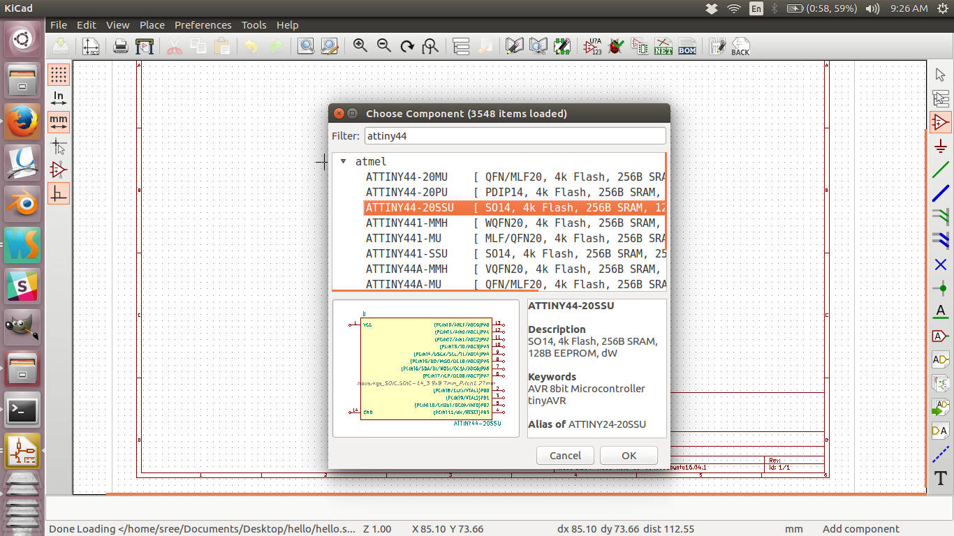
I have pulled out the attiny44 from the component library and added it to the sketch.
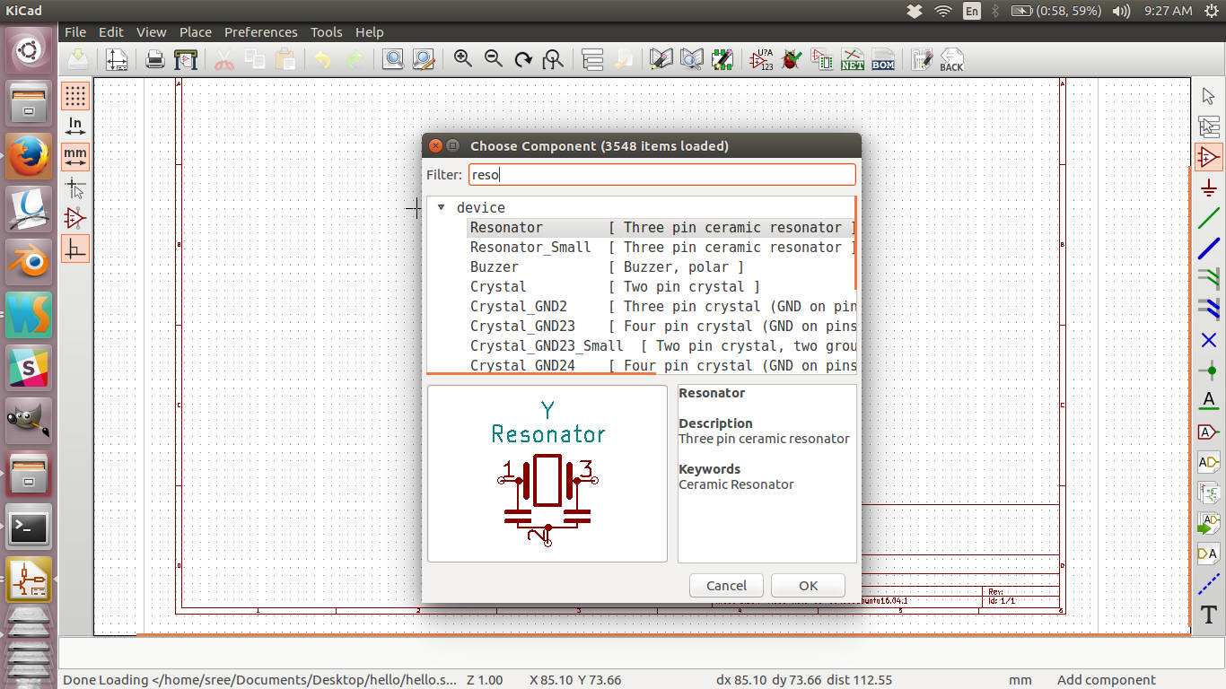
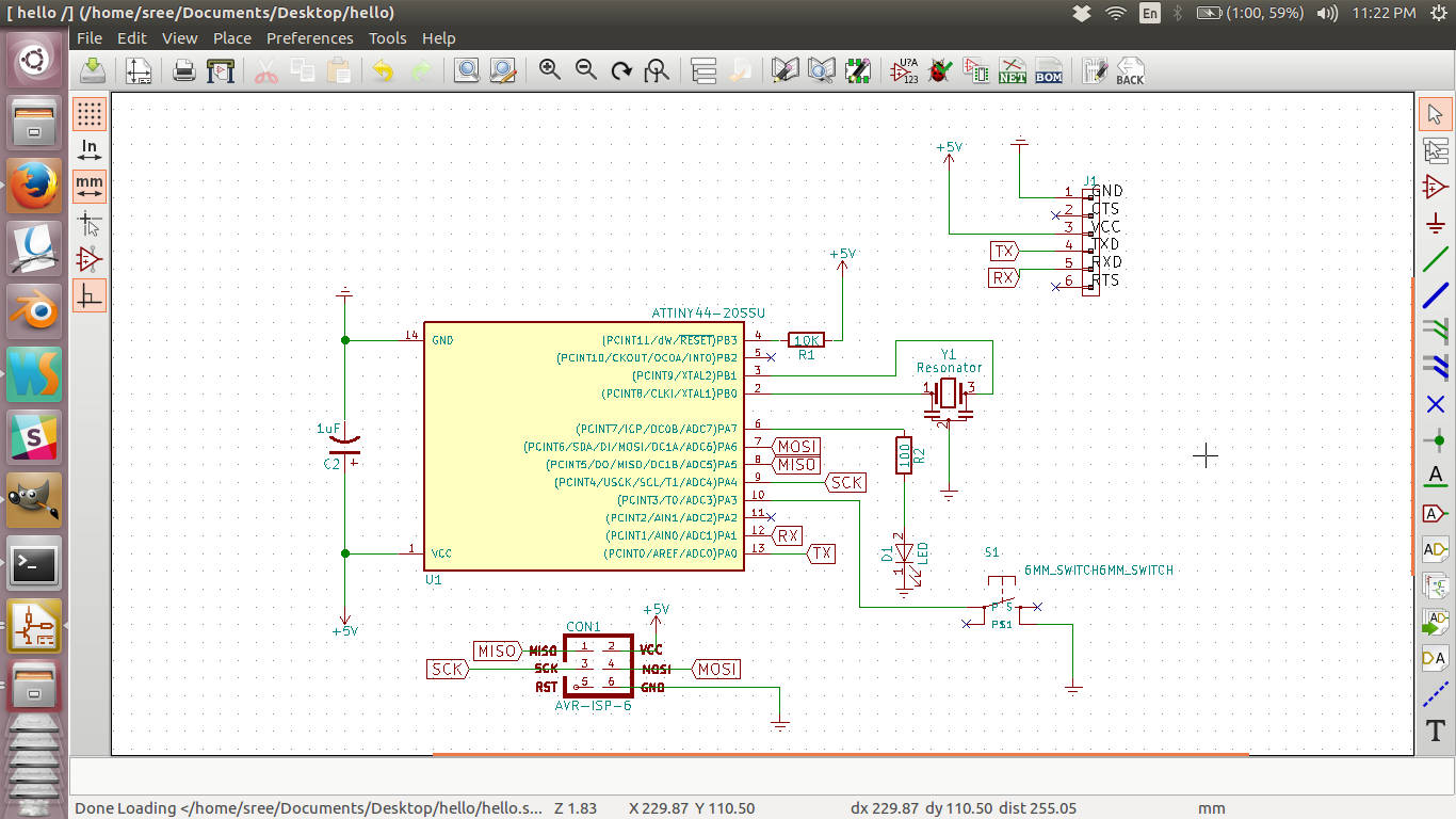
All the components where add to the sketch at propoer locations and they were wired togather to get the final schematic diagram. Note that labels with same names are considered to be connected, thought they are not actually connected in the diagram.
Now you can save the schematic and start creating the pcb layout. Before you go into the pcb layout. You need to save the netlist(the list of components used in the circuit), then map which types of pads you want to use for different compnentns in your circuit. ie, if you want to use SMD or through or different size of SMD and all that. Its called as the foot print of the component. You can do this association by clicking the "cvPCB" button on the tool bar. Here you can enable the preview and chose which footprint to use. You can even filter by library or name from the list. This feature comes handy as there are a lot of component in the list.
All the components and there footprints used in this circuit are not avaiable by default. you will have to manaully import them into kicad. This and this are the libraries needed and this link will help you install them.
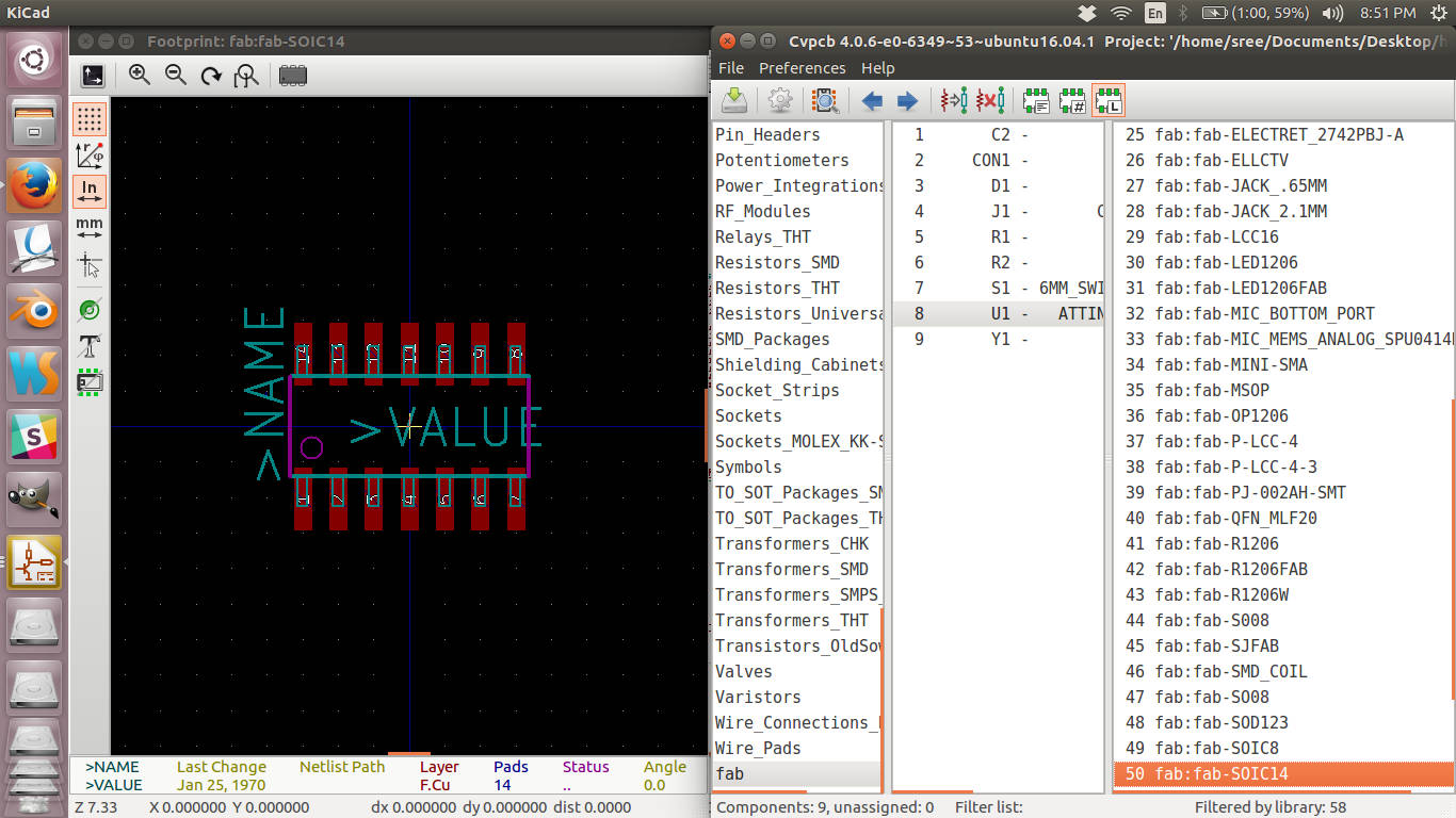
Associating components and footprints.
Finally create the pcb laytout file and import the schematic and you will get all the footprints. Now arrange them properly and make out the routes.
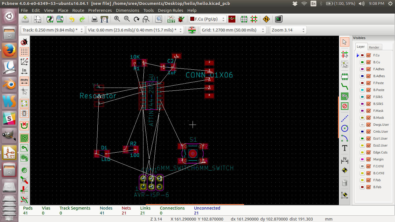
Routing the pcb.
KiCAD file archive
C1. Impressions
The user interface is not intuitive and is annoying at times. It opens a lot of windows and that adds up to the trouble. Functinality wise this is good. I do even see a 3d render functionality, though i have not used it.
D. Eagle
EAGLE is a scriptable electronic design automation application with schematic capture, printed circuit board layout, auto-router and computer-aided manufacturing features. EAGLE stands for Easily Applicable Graphical Layout Editor and is developed by CadSoft Computer GmbH. Cadsoft Computer GmbH was acquired by Autodesk Inc. in 2016 and now eagle is a part of autodesk. Read more about eagle at wikipedia
This is the most popular software used for electronics design. The
following Youtube
tutorials by Jeremy Burns helped me started.
Introduction to Eagle schematics
Introduction to Eagle PCB making
This tutorial shows designing a pcb from scratch showing all the process from making the schematics to
the designing the pcb. Here
a double sided board is made unlike our project which we use a single sided board. Except that it shows
all steps to do with eagle.
I followed this link
. Here it was shown how to modify the existing schemas and board layout but i dont wanted to do that. I
wanted to make the schema
from this image.
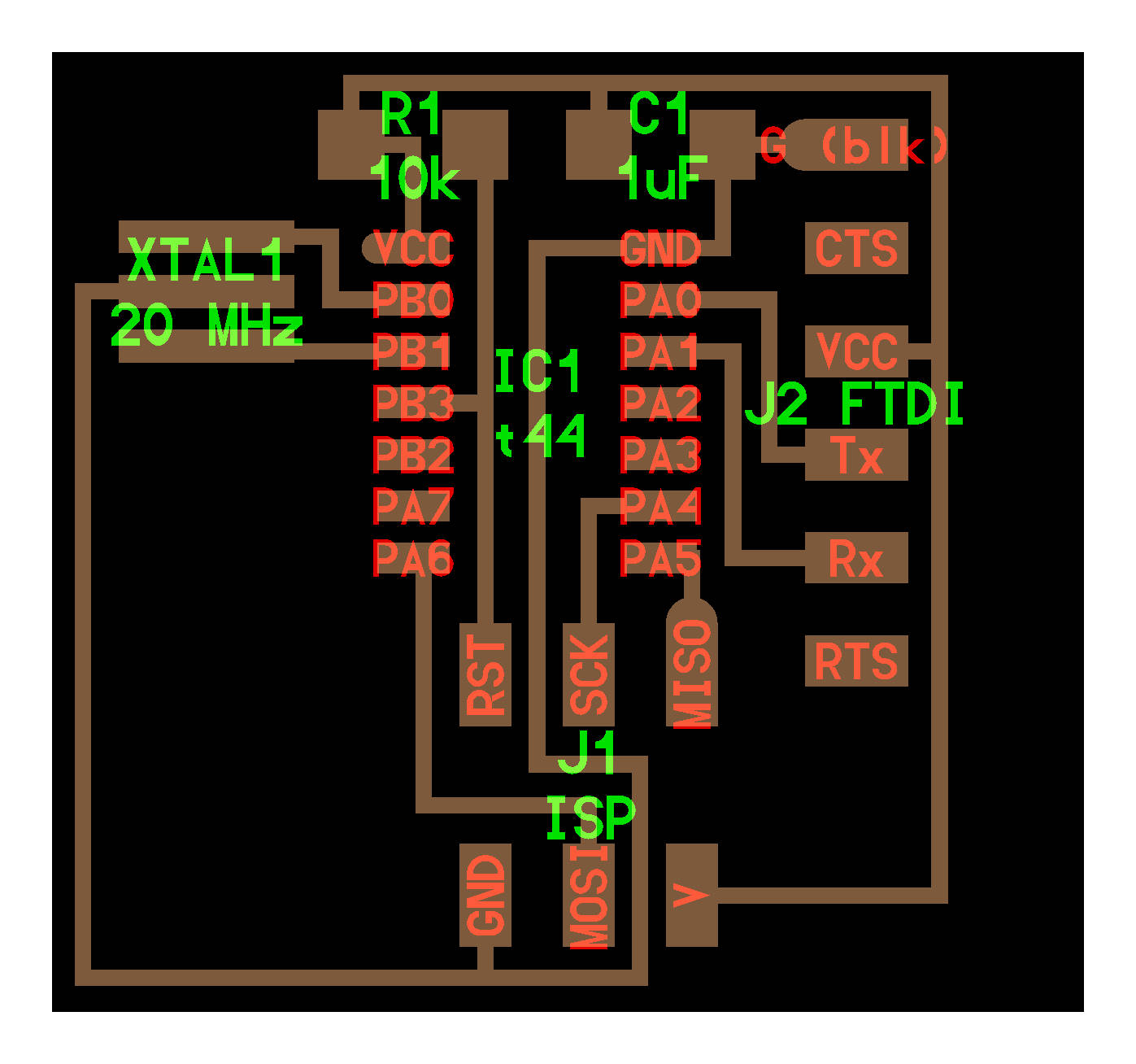
Neils board PCB layout
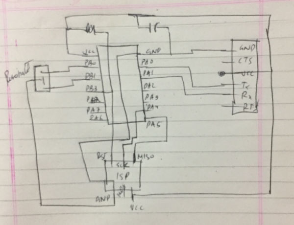
I made a drawings from the image
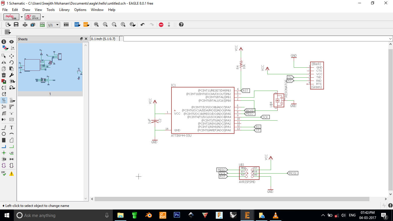
With this drawing in place. I opend up the eagle software and the following are the steps i followed.
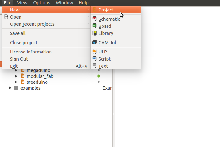
- Created a new project and schema
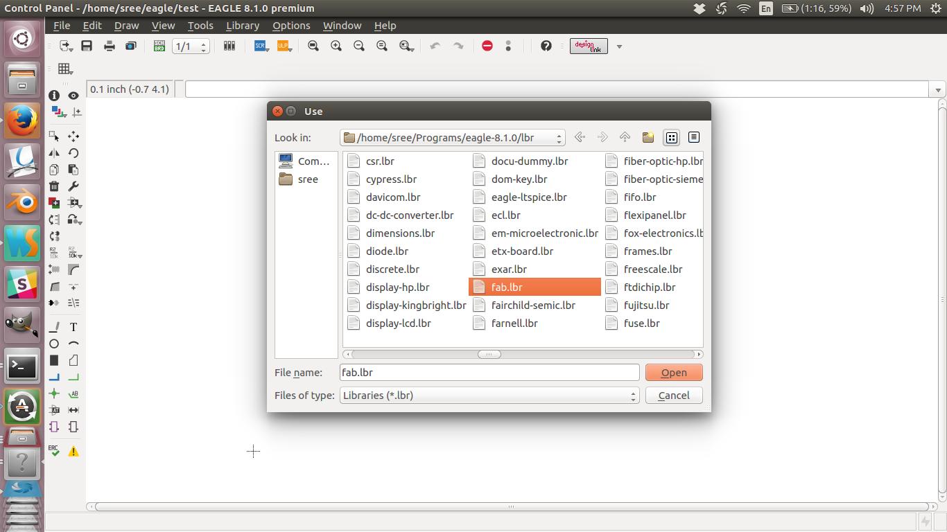
Crating a new project - Downloaded the library files from fab
- Extracted and copied the files into the eagle folder
- Loaded the library to be used in the project
Importing the library - Pulled out required components using the add tool. This can also be accessed with the shortcut ctrl+a
- Wired them up: There is a line tool which is used to make connections in the schematics. Using this tools you can make the connections. Adding and deleting connections and components are the most important part of using eagle. Clicking on the tool every time is not convenient.Its a good practice to make the shortcuts for commonly used tools. You can do this from 'assign menu' in 'options tab'
- Added the power supply and grounds
- Labeled the components and added remote connections between some
of them using the label tool. When two wire are given the same name the get connected automatically in eagle. I used my
drawing to assist me with the same
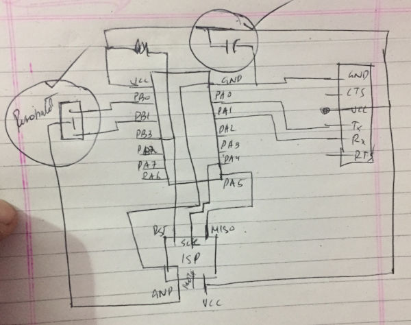
Marking added components in my drawing
Redraw of Neils board - Now finally i make the modifications, ie an led and a push button
to the design
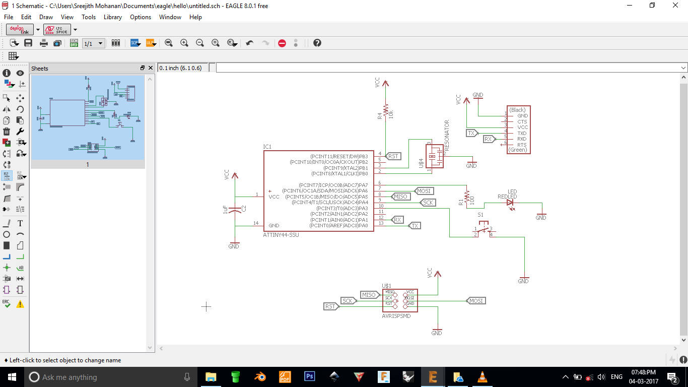
Schema edited with an lED and a push button
- It was time to create the board from the schema. When you do so by
clicking on the board view button,
eagle prompts to create a new board layout file and the follwing output is generated on
confirmation.
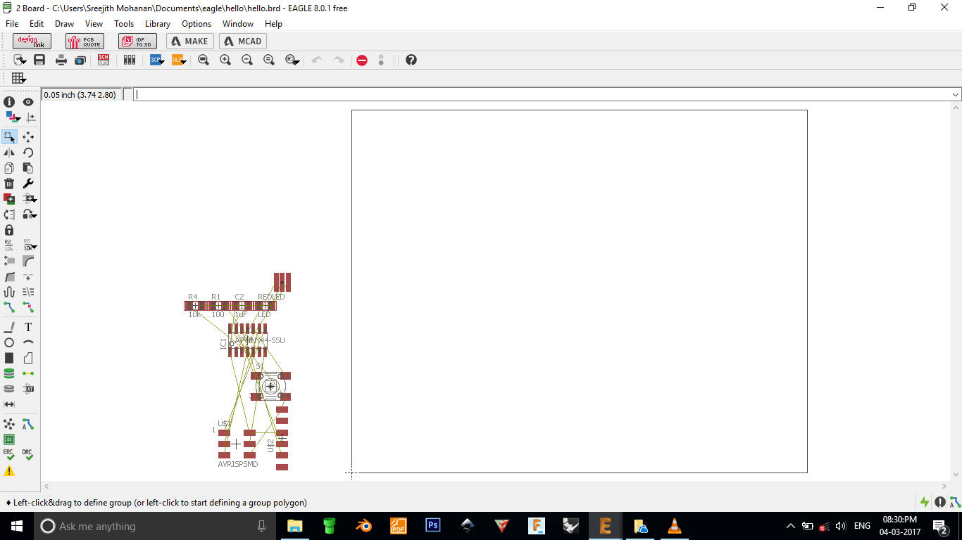
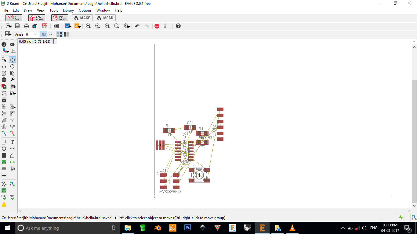
New board layout created from schematic diagram - Now i moved the components to insde the board.
Components moved inside the rectangle marking the board - There is a button in eagle tools panel for setting the design rules. Click on that and
change the properties in the panels as
shown in the images below. This will help you check your design for potential errors
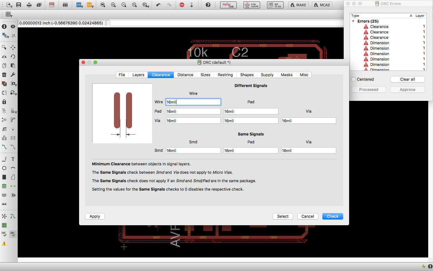
Clearence settings
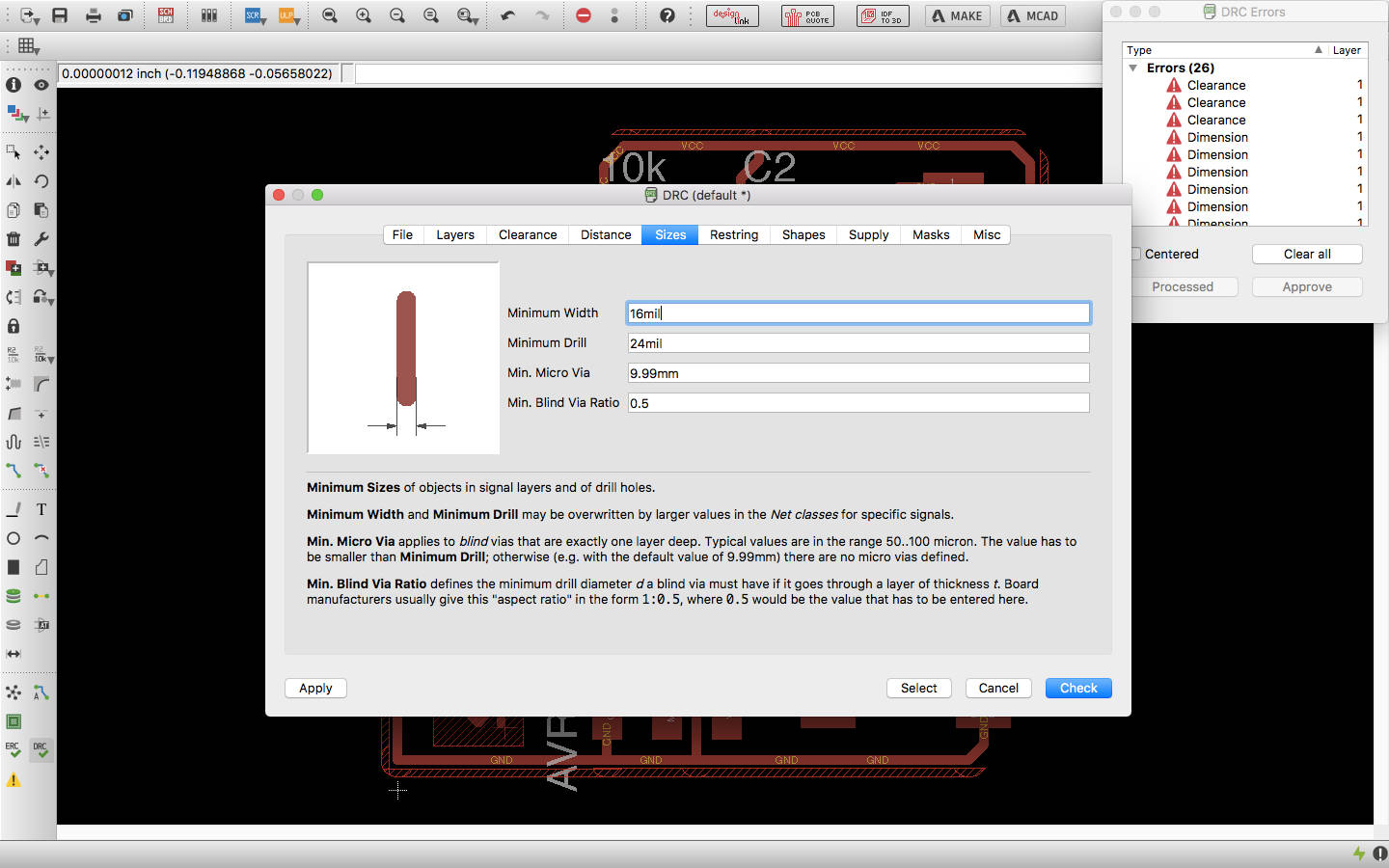
size settings
- Now i tried auto routing with the default settings by clicking on the autoroute button.
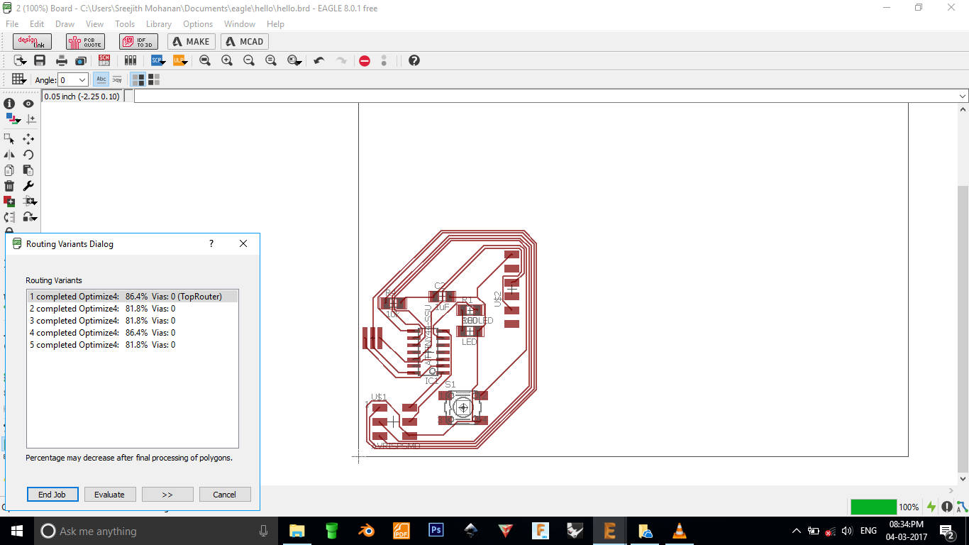
Autorouted pcb - As a learning initiative i droped the autorouted file and started
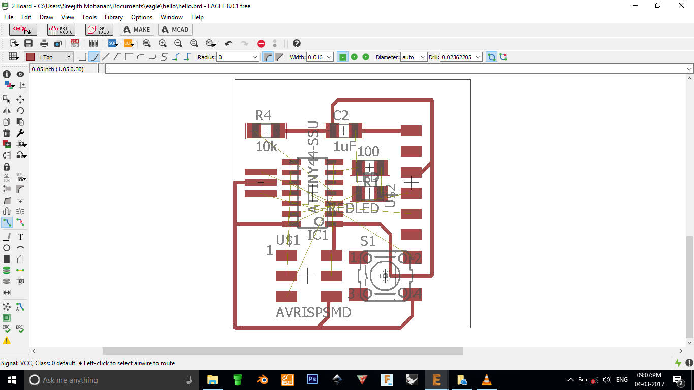
to do routing manually.
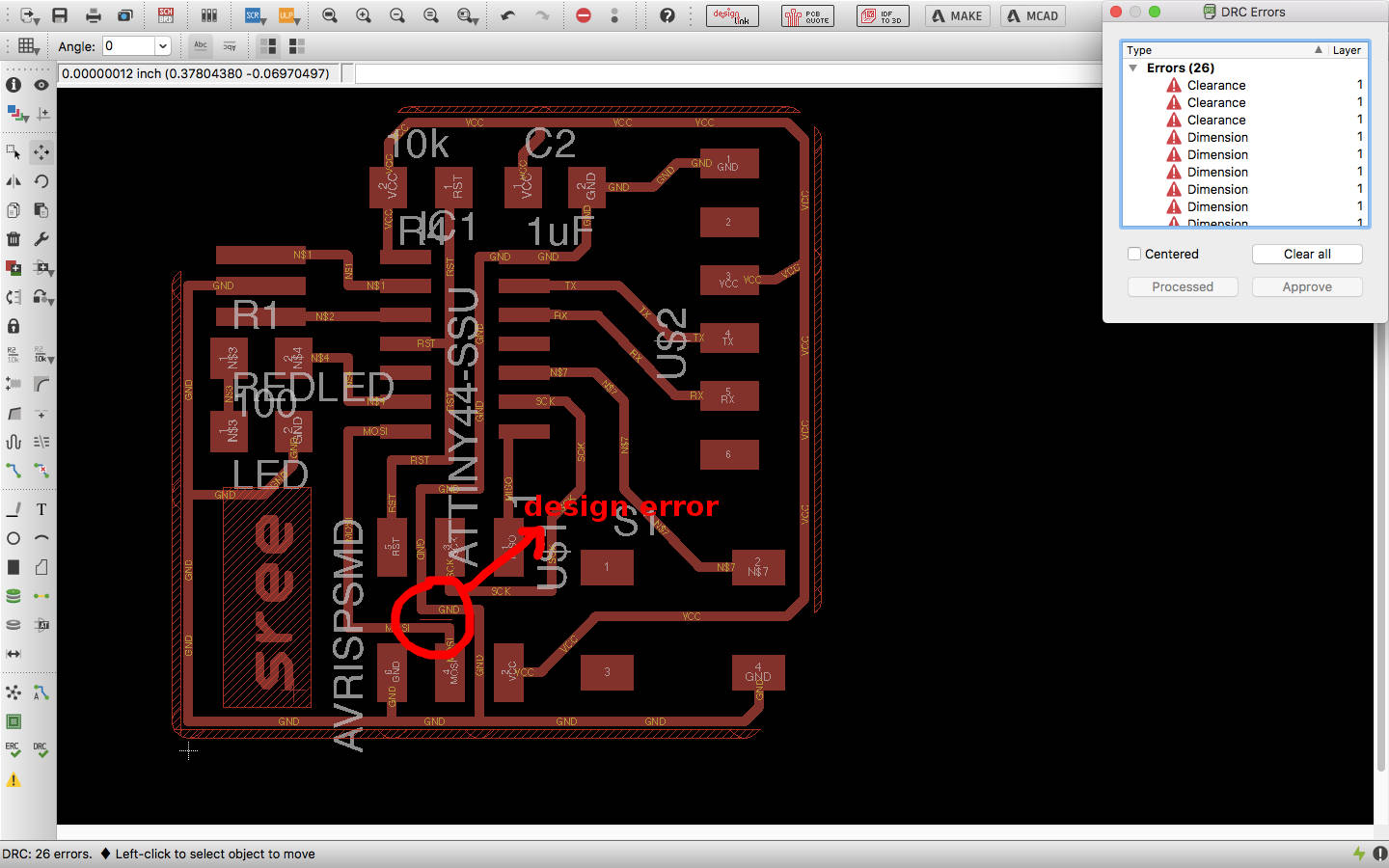
Manually routing the pcb - Once you are done with your routing, click on the DRC button on the tools panel and
click check. This checks if
your design is in correspondence with the rules you have set earlier. When i did this i had a few
errors. The border errors could be neglected but
the one labeled in the images cannot be, as it will cause a connection between wires in my board.
You need to move the wired a little bit and check for the
error. It will take a few iterations.
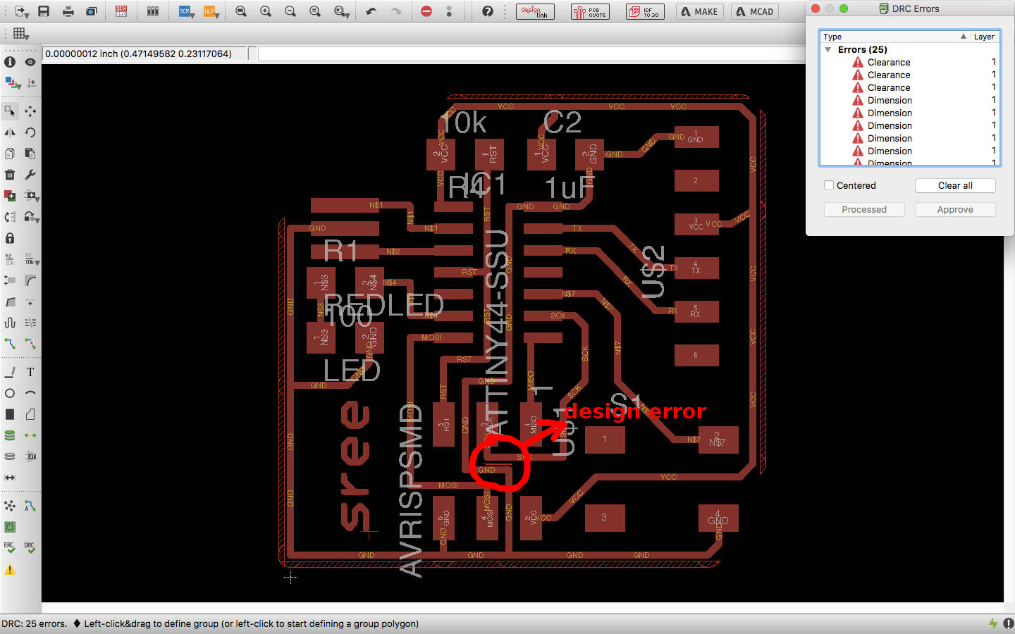
Design errors
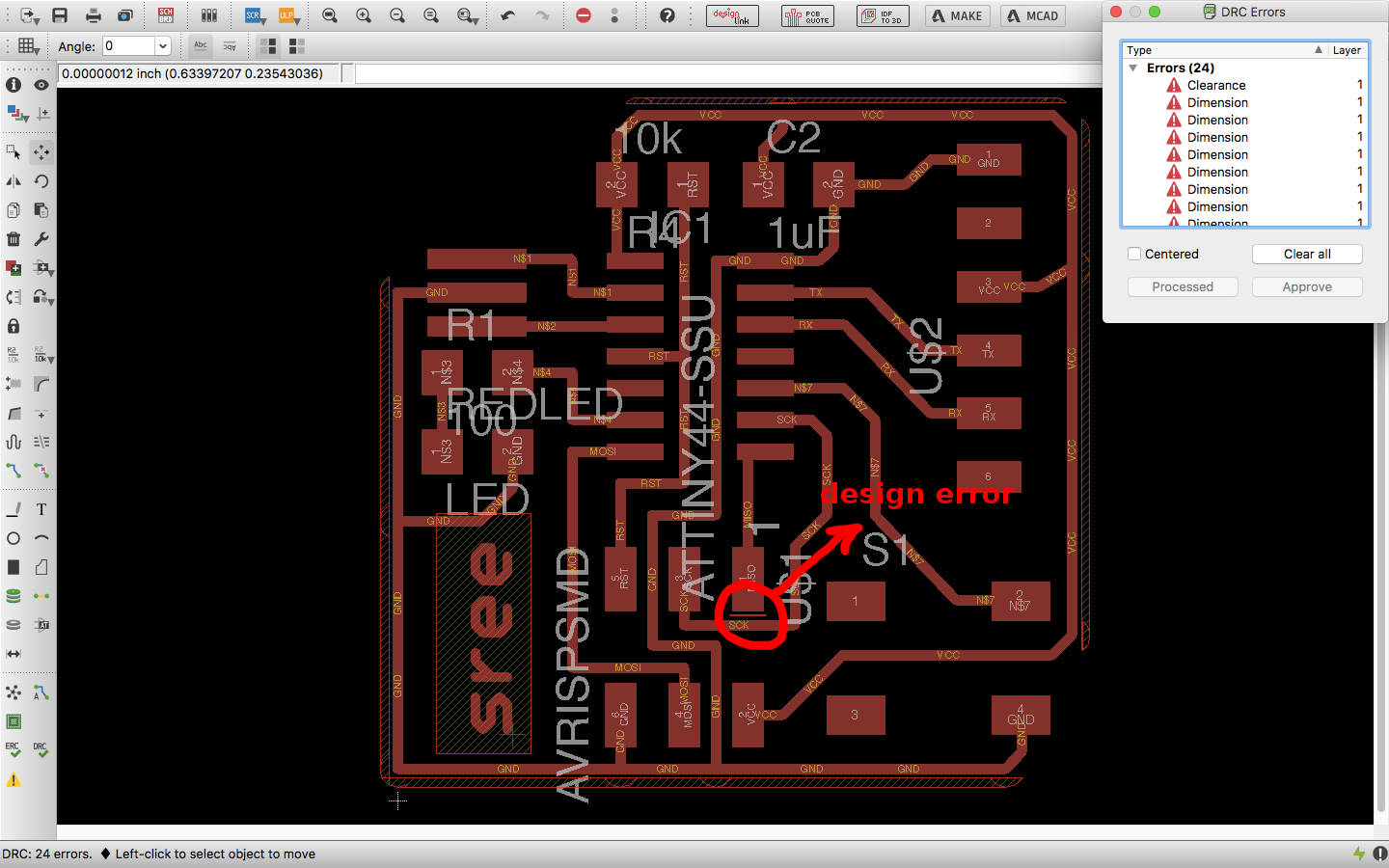
Error moved to a different location after moving wires
Error moved to a different location after moving wires
This was the major issue i faced during the design process. Dont proceed without fixing this error - After a couple of iterations i could get rid of that error. This
is
the final route. I have also changed the width of the border line which is used for cutting
reference to match our drill bit(0.032").
This can be done by selecting each line and right-clicking and choosing properties.
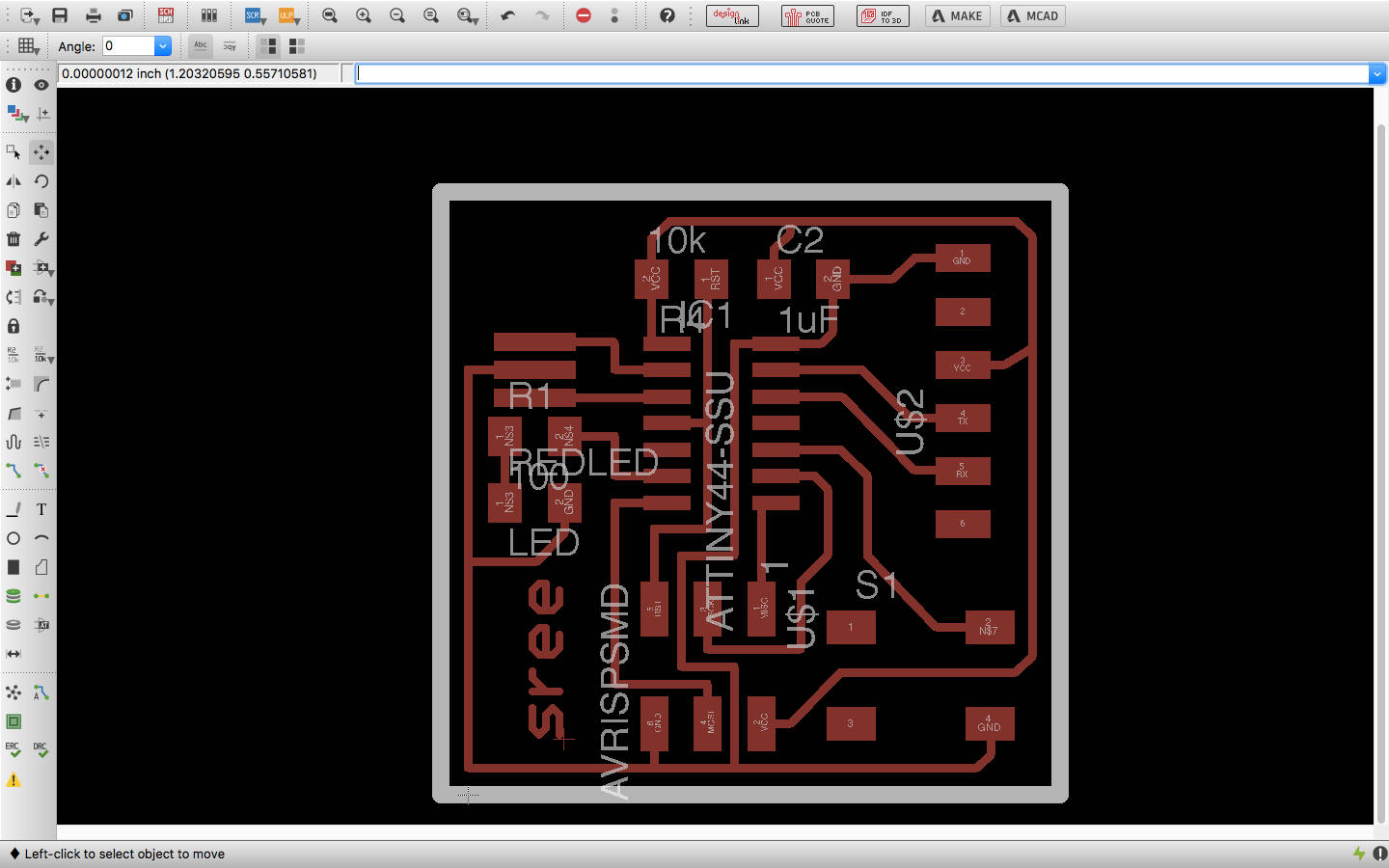
Image of the final pcb design
Schematic design file Board design file
e. Milling the PCB
- Now i exported the board into png each for the cutting and the
traces. While exporting
we need to first enable only the top layer in the layers panel and export the png. Then enable
diamesion layer alone and do
the same. Make sure that you choose 1000 dpi and grayscale image in the export panel. The exported
images are shown below.
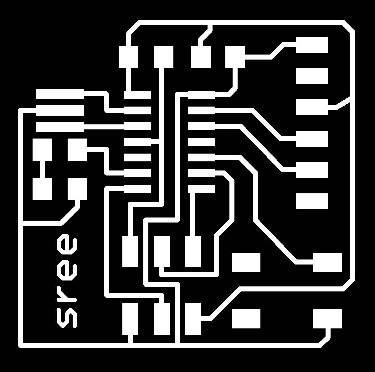
The traces file

The cut file - The cut file need to be inverted, i did that in photoshop

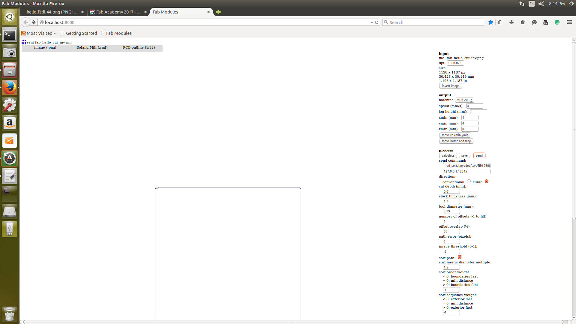
Inverted image - Now openup the mods in the computer connected to the milling
machine. Load the png, change a few settings( xmin, ymin to 4mm and error pixels to 1.0)
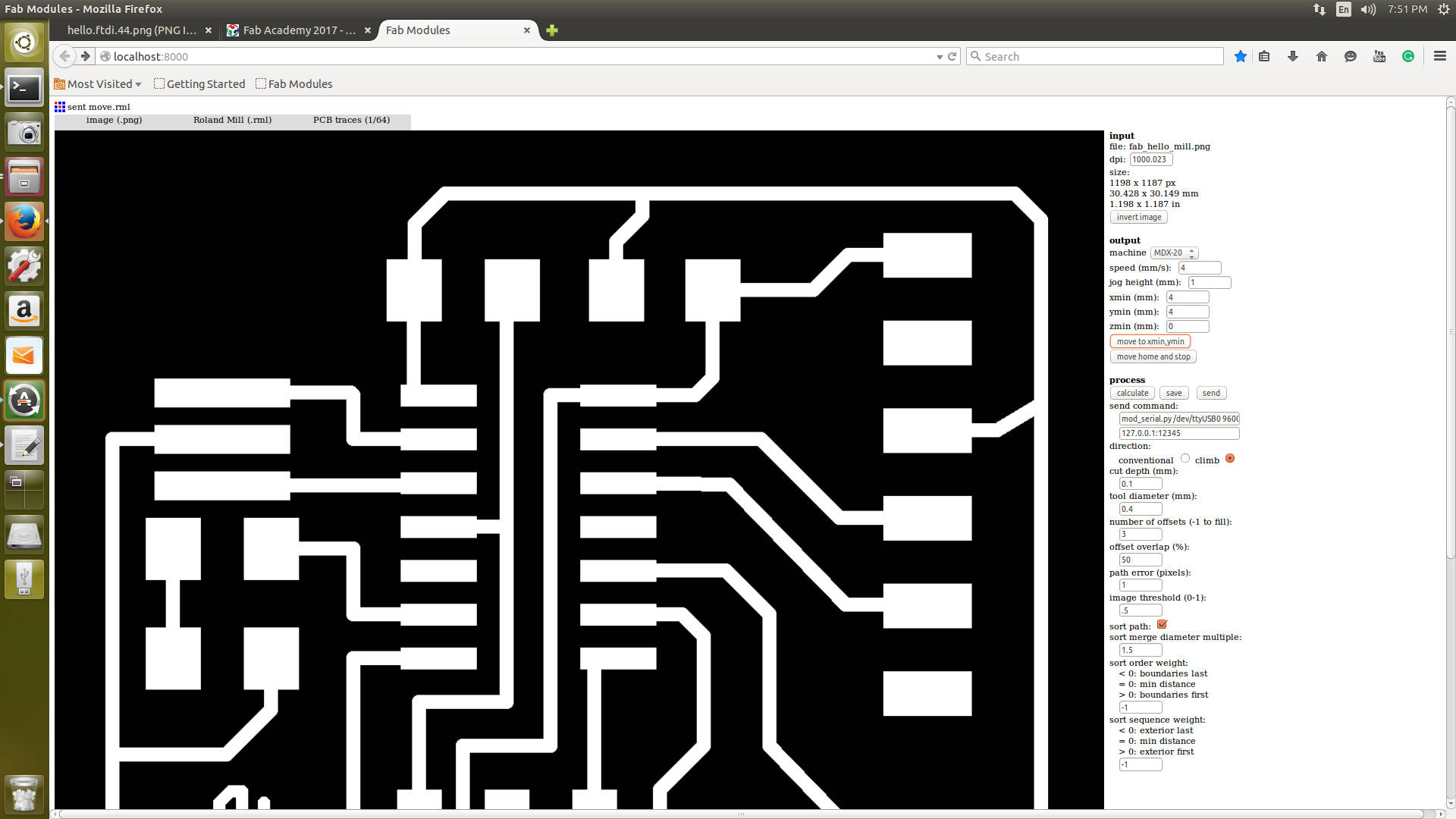
Milling settings -
Print the traces followed by cutting the pcb and later remove the unwanted copper
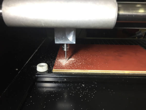
Milling the board
Cutting settings
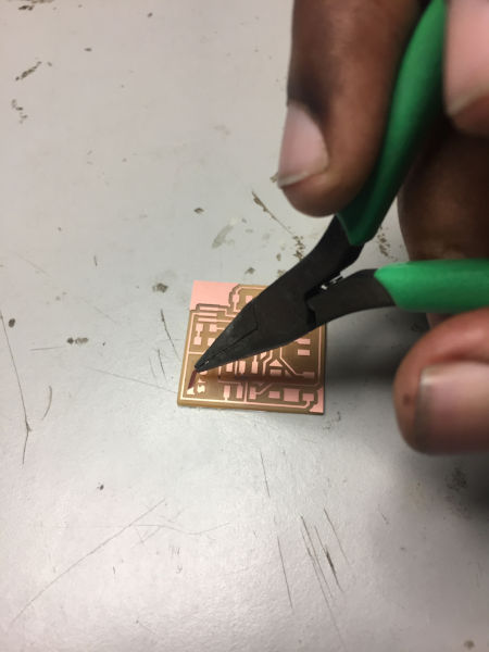
Pulling out the extra copper
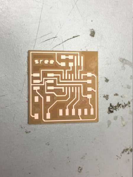
Final pcb
f. Soldering
Once you have your board ready it is time to solder the components into it. I collected the components as shown in the table below. Note that though i used green LED and 100 ohm resistor in my design i changed it to red in my board and therefor i hade to change the resistance to 499 ohms.
Here is how i calculated the resistance needed
The resistor in series with LED, so Voltage -Forward (Vf) is 2V and DC Forward Current of 10mA
(obtained from datasheet)
Calculating the required resistance:
R = (Vs - Vf) / Ifc = (5V - 2V) / 0.01A = 300 Ohms
I used 499 ohm which is the nearest availble in our lab close to this value.
| Sl no | component | quantity |
|---|---|---|
| 1 | ATtiny44-SSU | 1 |
| 2 | 20mhz resonator | 1 |
| 3 | AVR ISP SMD header | 94 |
| 4 | FTDI SMD header | 1 |
| 5 | 10K resistor | 1 |
| 6 | 1µF capacitor | 1 |
| 7 | RED LED | 1 |
| 8 | 499 ohm resistor | 1 |
Start soldering the components into the board.
Final PCB with components soldered
G. Programing the board
Once you have your board ready with all the components soldered in properly its time to test if the board is working properly by programming it.
- Download Neil's echo hello world program. Also download the makefile. Rename the make file from hello.ftdi.44.echo.c.make to "Makefile" without any extension.
- In the terminal move to the location the files are located and run
make
A .hex file will be generated. - Connect the ISP to the usb port and connect your board to the ISP.
Now run the following commands in the terminal.
make program-usbtiny-fuses
make program-usbtiny
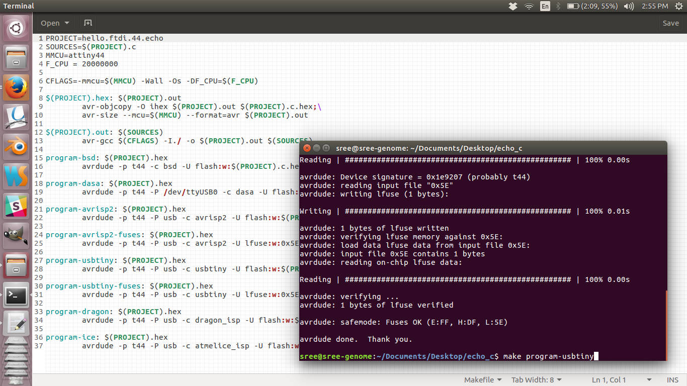
Output of running "make program-usbtiny-fuses"
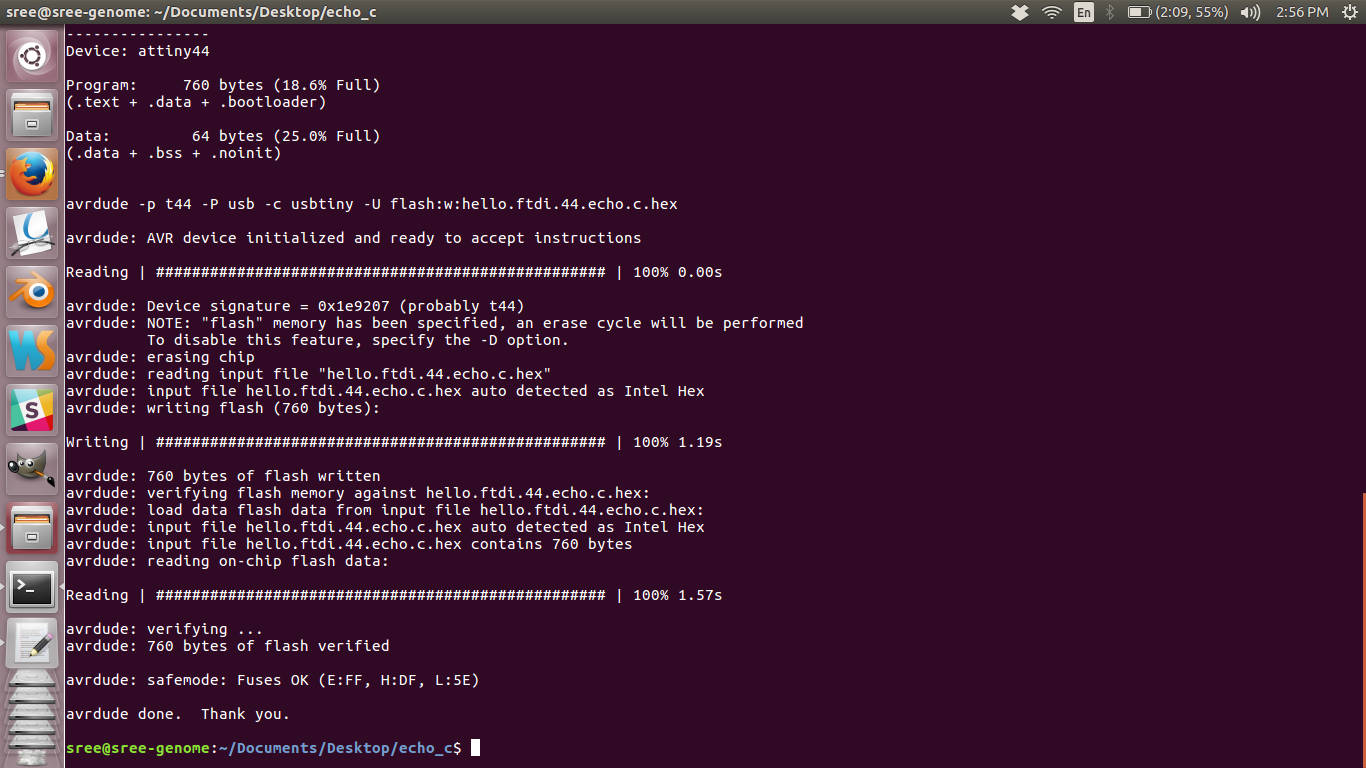
Output of running "make program-usbtiny"
The program should be burned into our board as the terminal shows a success message.
h. Testing the board
-
To test the board with the echo hello world program burned into it, we need a program called
cutecom. Install it by typing the following
command in the terminal.
sudo apt-get install cutecom - After installation run the program by running.
sudo cutecom
to open it with admin permissions. - Now connect your board to a usb cable and connect it to the usb port of your computer.
- On the cutecom UI click connect button, after changing "device" to
"/dev/ttyUSB0".Now the board will be connected.
In the textbox labeled "input" type some character and you can see the same being echoed back to
you.
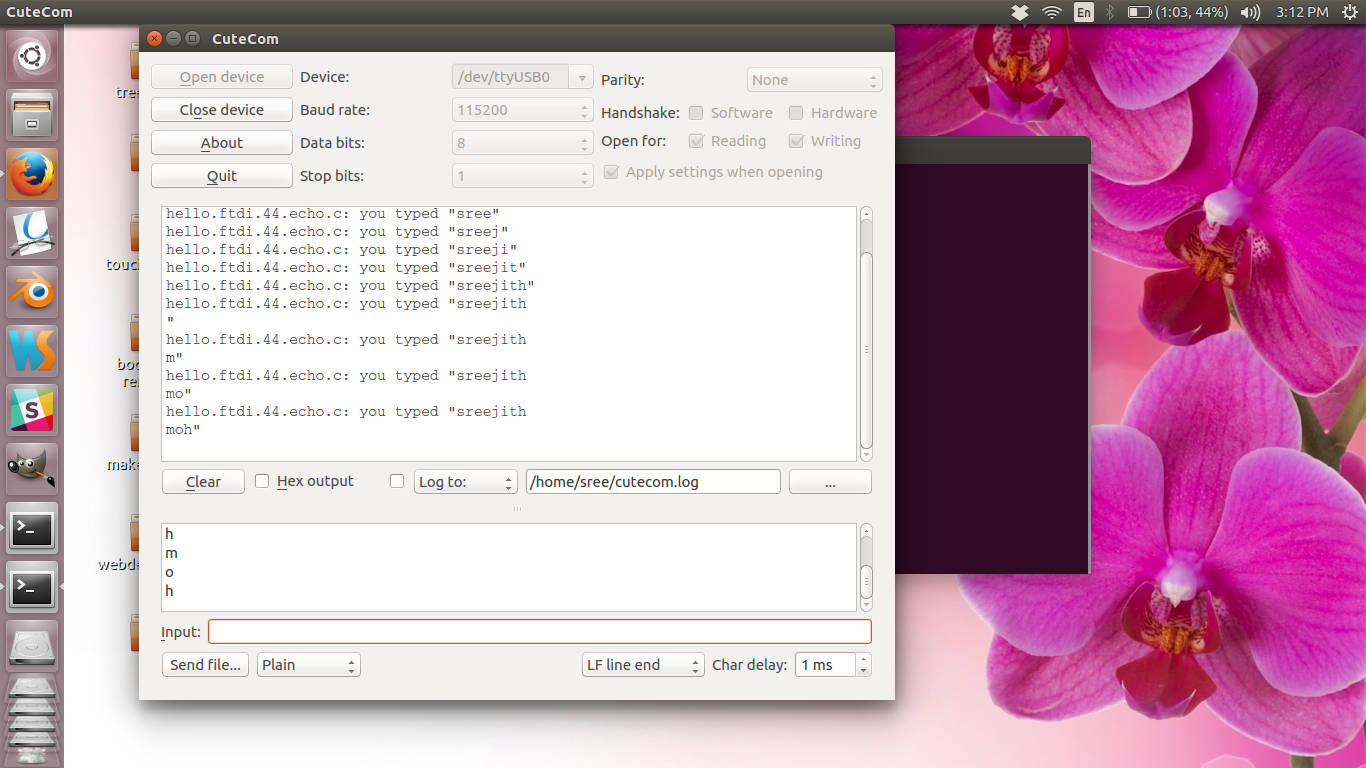
Cutecom output screen
That confirms that the board is working fine.
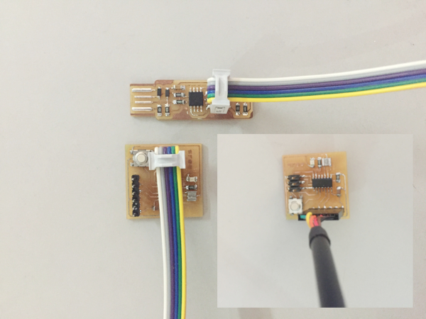
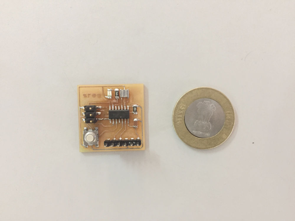
photographs of my board connected. This is the smallest board (3cm x 3cm) here ☺
i. Problems faces
While routing, some of the routes where not coming perpendicular, this was because of the grid settings being set to some big value. I found it useful to change this to a smaller value at times when you have this problem.
j. Summary
- Tried Kicad and eagle for pcb design.
- Re-made Neils board with an LEd and a push button
- Learned to used design rules in eagle
- Tried auto routing as well as manual routing
- Finally soldered and tested the first pcb i designed and made myself

This work is licensed under a Creative Commons Attribution-NonCommercial-ShareAlike 4.0 International License.