13. INPUT DEVICES
Index
- Assignment
- Introduction
- Understanding How sensors work in general
- Sensors i am using
- Designing the Board
- How datasheet helped me
- Making the PCB
- Time to Code
- Results
- Problems and Solutions
- Summary
A. Assignment
- Measure something: add a sensor to a microcontroller board that you have designed and read it.
B. Introduction
In this week we are working with input devices. We have a couple of thermistors, a hall sensor and a light sensor in the fab inventory. I plan to use all of that. Instead of making a micro-controller board for the purpose, i plan to reuse the board i have designed and made in the output week as a general purpose board. I will only make the sensor board as a seperate module and pin it on top of the existing board. This approach will help me learning modular designing as arduino does.
c. Understanding how sensors work in general
Sensors usually takes a sensory input and gives a corresponding voltage to that input. For
example the thermistors,
give different resistance depending on the temperature. This variation is linear(appx) and by reading
this voltage we can
extimate the temperature. The principle is same with almost all sensors but the only difference is that
some sensors give
higher voltage with higher input signal and other give lower voltage as the input signal increases.
Example for this is the
NTC and RTD type thermistors.
c1. Sensors i am using
I am using an NTC temperature sensor, the photoresistor and the hall sensor.
Hall senser
It is a transducer which varies its voltage in response to a magnetic field.
These sensors work on the principle of .
They are commonly used for proximity switching, positioning, speed detection, and current sensing applications.

A wheel containing two magnets passing by a Hall effect sensor; from wikipedia
More details
Similarly, the thermistor will help me measure the temperature, the photo resistor will help me
measure the intensity of light. You just get a voltage value from these sensors. We then need to find the corresponding value
of the temperature(for example) by trial and error. But today most of the sensers come preconfigured. ie, they are standerd meaning
a particular value of voltage refers to a particular value of temperature or the variable we are sensing.
d. Designing the Board
After going through the datasheet of ATMEGA328 i identified the ADC pins and i am
making the design taking care that the sensor pins go to these pins. Also proper potential division
resistors are provided.

Schematic diagram

Board layout
Schematic design file
Board design file
I am reusing the board from the output week. The design files are as follows.

Trace file of the MC board

Cut file of the MC board
Schematic design
file
Board design file
d1. how datasheet helped me
The pin diagram in the datasheet came handy while designing the pcb. It showed me where the adc pins where. The datasheet also helped me identify how the multiplexer in the microcontroller work and also helped me with the registers used to enable the and configure ADC
e. Making the PCB
Then i created the monochrome png images for milling and cutting. Those images in full resolution
are given
below.

traces image
cutout image
Later i used modella and fab modules to mill and cut the board. Then i collected necessary
components for the board and sticked them side by side to the printout of the
pcb which i designed. This is something i suggest while soldering. Make sure that you have a
printout of the pcb with components and also have the components sticked corresponding to their name
and value. This will save a lot of time. Finally i started soldering and successfully soldered all the
components. This is the finished board pinned through header to the microcontroller board.
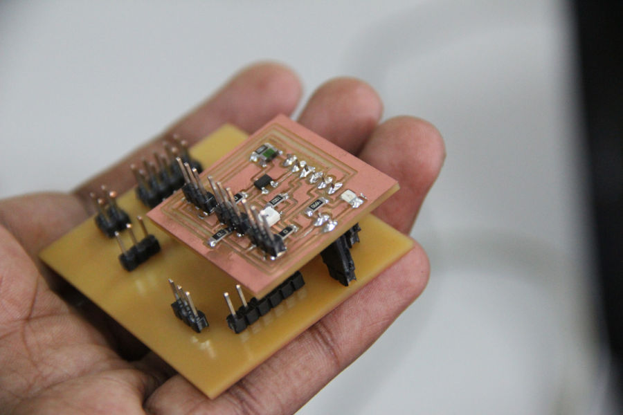

Final Board
So basically this pair of boards consists of a atmega328 microcontroller and 3 sensors. The sensors are on the top board.
I am unsing a 10k resistor together with the thermistor and the phostoresistors as potential dividers.
This sernsors give anolog data which will be read by the ADC hardware and get converted into corresponding value between 0 an 1023.
This value will be displayed on the ldc.
f. Time to Code
Now i have everything setup. Its time to write the program which reads the sensors.
I am using the LCD library i made in previous week to display the sensor readings in it.
The following is the code. Each important code is documented with comments. This code displays given
the values of the sensor in the LCD display.
The code uses the ADC (Analog to Digital conversion) feature of the micro controller.
As i am using mltiple sensors at once employing multiplexing. For more details about ADC and
multiplexing refer these links.
Introduction
to the Analog to Digital Converter (ADC)
Reading the
Potentiometer
Getting the Full 10-bits from the
ADC
f1. Register description
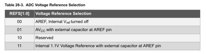
- ADMUX - ADC Multiplexer Selection Register

- Bits 7:6 – REFSn: Reference Selection [n = 1:0]
These are the register which help setting the voltage reference for the ADC.The following table shows the value and the voltage used as reference.
- Bit 5 – ADLAR: ADC Left Adjust Result
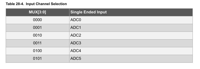
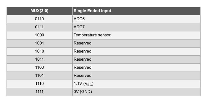
This bit affects the way in which the adc value will be presented in the ADC data register. When written 1 the result get left adjusted, else the data is right adjusted - Bits 3:0 – MUXn: Analog Channel Selection [n = 3:0]
The value of these bits select which analog inputs are connected. Refer table below
- Bits 7:6 – REFSn: Reference Selection [n = 1:0]
- ADCSRA - ADC Control and Status Register A
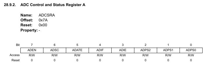
This is one of the most importent control registers.
- Bit 7 – ADEN: ADC Enable
This bit enables ADC. Remember that turing this bit OFF during a conversion will terminate the conversion - Bit 6 – ADSC: ADC Start Conversion
In single conversion mode(the one which we use here) writing 1 will start ADC conversion - Bit 4 – ADIF: ADC Interrupt Flag
This bit is set when a conversion completes - Bit 3 – ADIE: ADC Interrupt Enable
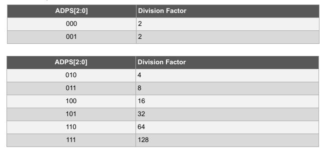
This bit will enable interrupt. Remeber that to enable global interrupt when using interrupt. - Bits 2:0 – ADPS2:0: ADC Prescaler Select Bits
This bit determine the division factor between the clock freequency and input clock for ADC.
- Bit 7 – ADEN: ADC Enable
- The ADC Data Register – ADCL and ADCH
These registers store the actual conversion data. As discussed earlier the ADLAR bit will determine if the data is left or right adjusted.
adc.c
- #include <avr/io.h>
- #include <avr/interrupt.h>
- #include "LCD_lib.h"
- int main(void){
- InitializeLCD();
- PutStringAtLocation(1,1,"X:");
- PutStringAtLocation(1,2,"Y:");
- // selecting prescalar
- ADCSRA |= 1<<ADPS2;
- // set reference voltage to AVCC
- ADMUX |= (1<<REFS0) | (1<<REFS1);
- //interrupt enable
- ADCSRA |= 1<<ADIE;
- // enable adc
- ADCSRA |= 1<<ADEN;
- sei();
- // start conversion on ADC 0
- ADCSRA |= 1<<ADSC;
- while (1)
- {
- }
- }
- ISR(ADC_vect)
- {
- uint8_t theLowADC = ADCL;
- uint16_t theTenBitResult = ADCH<<8 | theLowADC;
- //the last 4 bits in ADMUX determine the current adc channel. But we cant
- // just take the last 4 bits alone so its better to take the full hex
- // and compare. ie, 0b1100 0000 = 0xC0 and 0b1100 0001 = 0xC1
- switch (ADMUX)
- {
- case 0xC0:
- PutIntegerAtLocation(4, 1, theTenBitResult, 4);
- //change the channel to the next one
- ADMUX = 0xC1;
- break;
- case 0xC1:
- PutIntegerAtLocation(4, 2, theTenBitResult, 4);
- //change the channel to the next one
- ADMUX = 0xC0;
- break;
- default:
- //Default code
- break;
- }
- ADCSRA |= 1<<ADSC;
- }
ADC explanation and code review
The micro controller has an in build analog to digital converter. It can either be used in 8
bit or 16 bit modes.
This part of the micro controller simply takes in the input voltage and compares with the reference
voltage at the Vref pin. In 8 bit mode, if
the given voltage is 0 volts the ADC gives 0 as output. If we give 5 volt then the output will be 255.
If 2.5 volt is given then we get 125.
Thus we can get a value corresponding to each input voltage between 0 and Vref(usually 5 volts). Now
when we gives the micro controller an analog
signal, which is in-fact a varying voltage, The adc compares and finds the value as fast as possible.
The ADc is quite fast to do thousands of
conversion in a second and thus we can use this feature to measure analog signals. Now remember that
there is a little bit of approximation
as the ADC has limited bit resolution.
ADC is quite a huge part in a micro controller. Its hard and costly to make ADC hardware, so the makers
did'nt put many ADC in a micro controller.
But just hard wiring this big piece of silicon to just a pin is not good. So what they have done is that
the made 'Multiplexing'. Ie the ADC hardware
can be shared among many pins but the conversion happens one at a time.
That means i can use ADC in 4 different(number of pins depends on the MC) pins but at a time one pins
signal will only get converted. Ie first pins signal get processed first
then the second and so on. This happens thousands of times a second that we dont recognize that there is
only one ADC hardware doing all the job.
Here i am using the multiplexing functionality in the Atmega328 to read voltage at 2 different pins at
at time. I reuse the hardware and the LCD
library to display the value sent from the ADC on the LCD. Now you can read the code and the comments to
get a clear idea of what the code is doing.
For more details on the registors and how to configure them, refer the datasheet.
ATmega32 has ADC with 10 bit resolution, that means we get a value between
0 and 1023 for voltage between 0 and 5 volt. This is quite a good resolution
for this chip.
Here you can see that i am using ADC in free running mode and is utilizing multiplexing to read sensor data from two different pins.
Source code
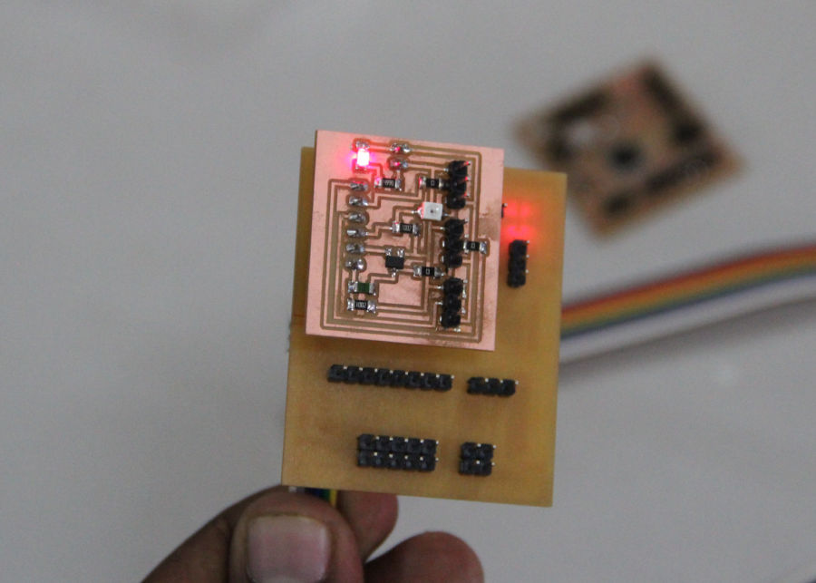
g. Results
I can sense the readings from the sensors and display them in the lcd display.
Final result showing the reading from temperature sensor
Final result showing the reading from hall sensor
h. Problems and solutions
- ADC( Analog to Digital Conversion) can be quite noisy. The ideal thing to do is to give a seperate voltage reference and power the adc with a seperate power source. The common power rail will have much noice due to the clocks and timers running inside.
- ADC is a slow process, thus when you are using the same processor for other operations the whole operaion can be slowed by adc. Take special care while using ADC
- IF you need extra precision, then there is an option in atmega328 to make the MC into a sleep mode where other operations will be at sleep and ADC can run smoothly
i. Summary
- Learned to use Analog to Digital conversion and multiplexing in the micro controller.
- measured the readings of three sensors simultaneously and displayed in the LCD.

This work is licensed under a Creative Commons Attribution-NonCommercial-ShareAlike 4.0 International License.