~ In-circuit serial programmer production page.
~ post date: 2017.2.20, recent update: 2017.2.25
A printed circuit board (PCB) supports and connects electronic components via conductive tracks, pads, etc etched into copper which is laminated onto non-conductive substrate. PCBs can be single-sided, double-sided or even multi-layered. The electronic omponents (capacitors, resisters, processors, connectors, LEDs, etc) are soldered onto the copper zones of the PCB, a process known as stuffing. Once everything is properly connected, the microcontroller needs to be taught (programmed), which typically requires a programmer. This project involves three phases: milling the printed circuit board (PCB), stuffing the electronic components, and teaching the microcontroller to be a programmer.
Milling a circuit board
The PCB is composed of a thin layer of copper, measuring in just microns of thickness, laminated onto FR1, phenolic paper. The pattern of copper connects a series of electronic components with electricity. If any unintentional connections are made, the whole system may be fried. While in subsequent posts, I will explore designing the etching patterns, this time around, I am using an open-source project developed in the FabLab ecosystem: the FabTinyISP version of an AVR ISP programmer/board. You can download the same PNG files I used for the traces and the board outline and read detailed build instruction on the FabTinyISP page or directly:
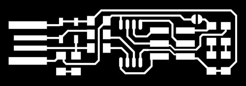
♻ FabTinyStar - Traces (1000 dpi) ♻
♻ FabTinyStar - Outline cutout (1000 dpi) ♻
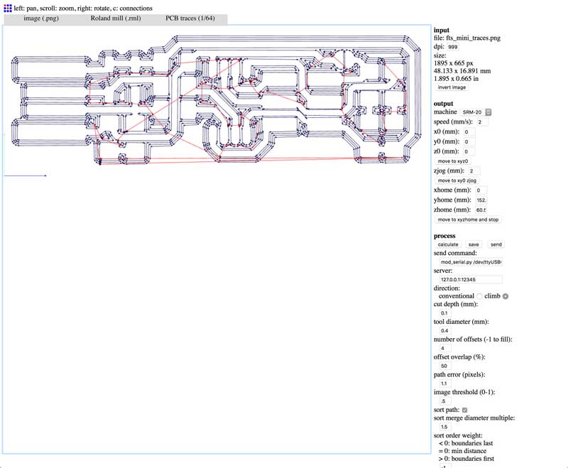
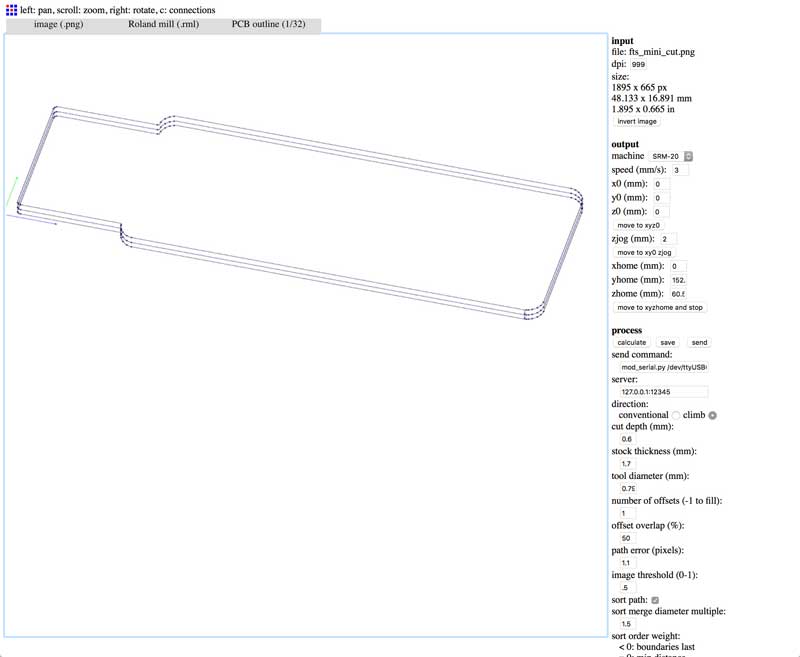
The first image is the traces. The white area will be copper conductive tracks, pads and an USB connector on the left. I will direct the mill to cut away copper around these zones, starting on the edge of the white and working outward. The second, the outline, will be a rough cut through the copper lamination and FR1 substrate. For the outline, the mill will cut a series of overlapping, successively deeper cuts until it clears the substrate.

The image files need to be converted into instructions for the CNC table top mill. This is delivered in the language of paths. Using Fab Modules, you can upload an PNG file (and many other file types), dictate Roland mill, choose the machine type (in FabLabO's case, SRM-20) and the module will output a file for the mill. Fab Modules produce files for different processes using machines typically found in Fab Labs. Setting for milling the traces, use a slower speed: 2mm/s. The outline can be faster: 3-4mm/s. Also set the zjog, the distance the mill head moves above the milling surface between paths (represented by red lines in the image below). A lower zjog will result in a quicker job. Too low, and the endmill may scratch the surface between paths, especially if the surface happens to be warped. More on that later. I set the zjog to 2mm. For the traces, the cut depth only needs to slice through the copper, which is measured in microns of thickness. The tool diameter is based on the end mill that will be used. If there are problems with paths not flowing through certain zones of the PNG, it may be due to that zone measuring inside the diameter of the end mill. The number of offsets, or number of paths the mill cuts emanating from the white zones, is a variable dependent on what is required of the PCB design. For instance, in this design, after cutting, a small bit of copper will remain to the left of the center two USB connectors if only cutting three offsets. That copper will need to be simply removed by a knife and saves time milling. Overlap is the percentage of the end mill that will cut over an existing cut path. Other settings are automatic or set locally on the machine.
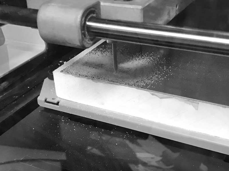
Some slight differences need to be accounted when cutting the outline. First, the cut depth defines the step down of each cut. Second, stock thickness is the thickness of the material plus a little extra to ensure the cut goes all the way through. In the image, the paths are stacked vertically representing successively deeper cuts. The mill is unable to cut through the entire depth of material in one sweep.
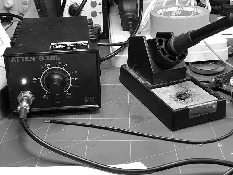
To preserve the end mills, it is critical to ensure the material is not warped whatsoever. Apply double sided tape across the entire back surface and adhere the FR1 (copper side up) onto the milling substrate, a chunk of high density foam.
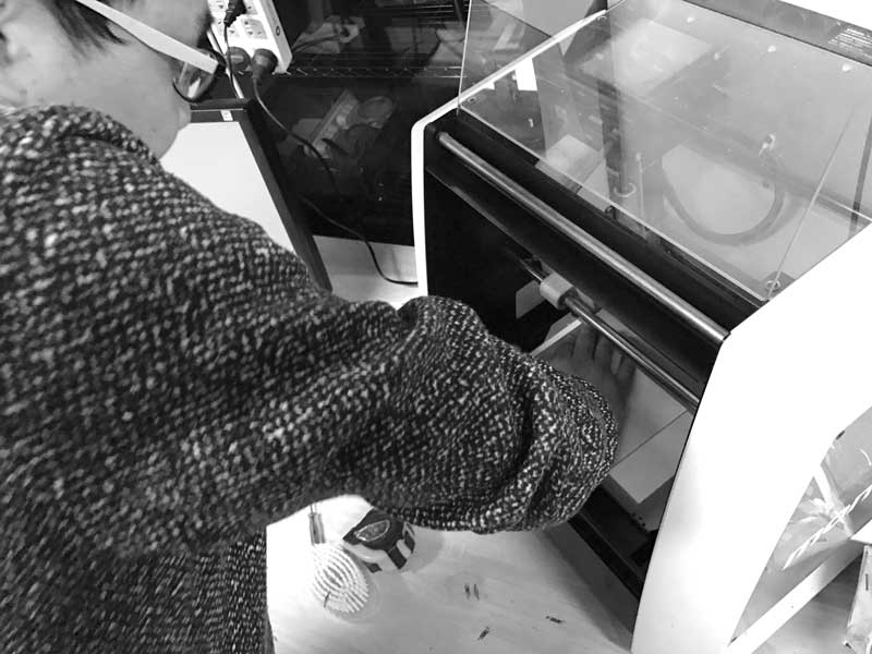
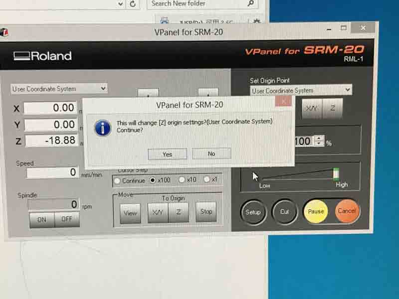
The output files need to be uploaded to the mill via a simple application, here: VPanel of SRM-20. The traces are milled first. This uses a 1/64" endmill which is carefully loaded into the mill head. Before starting the job, set the XY and Z origins by manually maneuvering the end mill to the desired lower-left corner of the job. Then slowly lower the endmill near the surface, check that the XY coordinates are as tight to the area of unused material as possible then set XY origin. Finally, manually reset the height of the bit (loosen, gently drop down, tighten while holding the endmill to ensure it does not move upwards). Set the Z origin before moving the bit up a few millimeters. Now the mill is prepared for cutting.
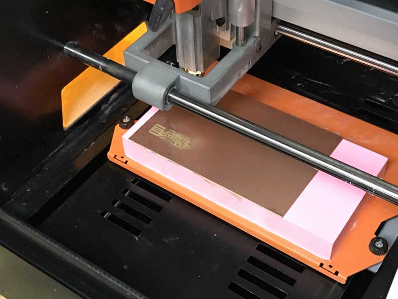
Mill the traces. Thoroughly clean the excess debris in and around the mill with a shopvac or similar. A well-maintained mill is an operational mill. Then change the end mill for the outline, in this case 1/32". Reset the Z origin in the same manner as before. Cut.
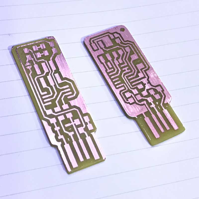
Sometimes many files are forgotten on an OS's desktop with nearly identical names for similar jobs. I milled a similar ICSP. Not the one I wanted. I planned to move forward with it regardless but I was talked out of it by fellows in the lab for fear the soldering would be too difficult for a first timer and the microcontroller this board was designed for was not as capable.
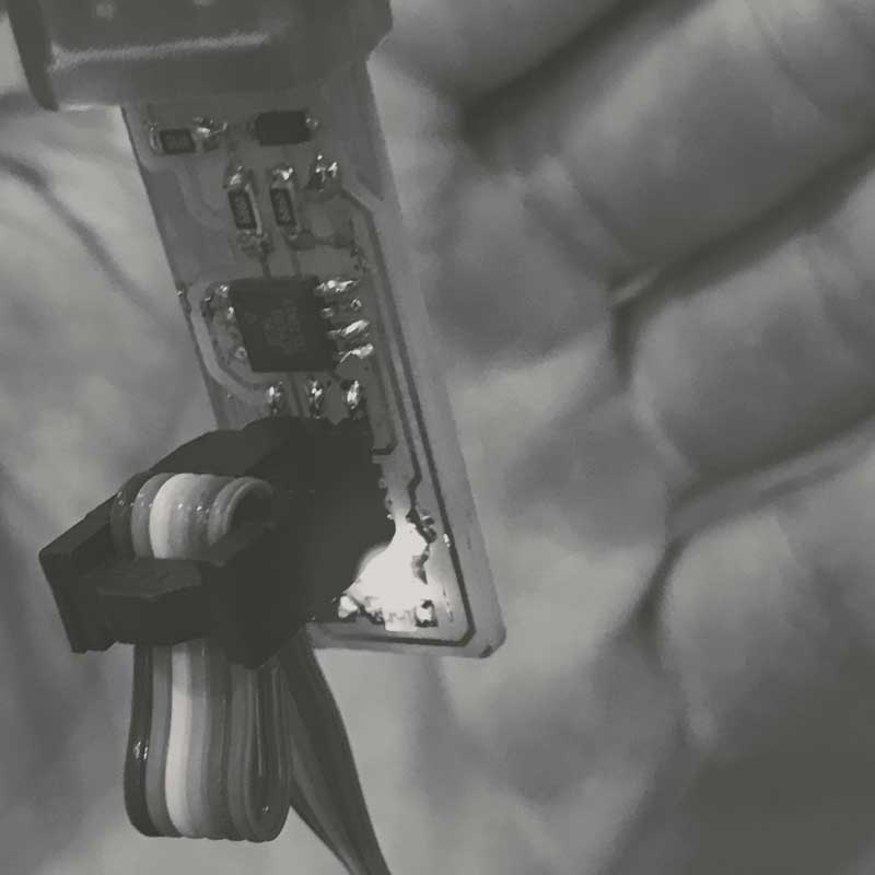
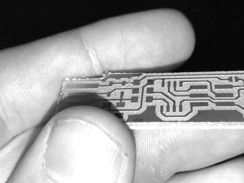
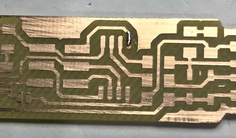
The PCB is cut. Deburr the board: Scrape the copper until it is shiny with a straight edge, like a utility blade, and clean of debris from milling. Then wash it with soap and water. Oils from our hands may slowly etch the copper over months. A working ICSP might become faulty.
I will post links to resources I have found helpful here.
Stuffing the board
Freshly produced PCB in hand, it is now time to solder the electronic components. Soldering is tricky. Repetition is key. I am beginning to find an effective method varying my practice, trial and error. This is a road map of component placement from the FabTinyISP page.
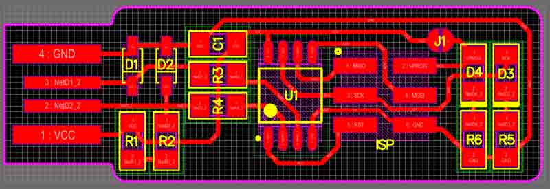
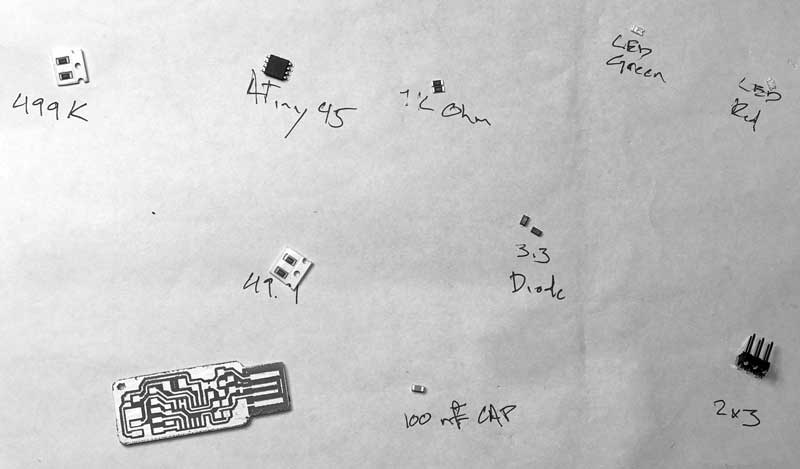
First, gather the components, or do not. I soldered two boards. The first, I gathered everything beforehand, the second time I grab componenets from their storage as I went along. Whatever, both worked. Just be careful not to lose any or return to the wrongly marked storage. The microcontroller and diode components are directional; all others are nonspecific.
- U1 : 1x ATtiny45 or ATtiny85 (directional)
- R1, R6 : 2x 1kΩ resistors
- R2, R5 : 2x 499Ω resistors
- R3, R4 : 2x 49Ω resistors
- D1, D2 : 2x 3.3v zener diodes (directional)
- D4 : 1x red LED (directional)
- D3 : 1x green LED (directional)
- C1 : 1x 100nF capacitor
- IDC : 1x 2x3 pin header
Preheat your soldering iron to around 400 Cal and make sure the tip is clean. When soldering heat the the tip of the connection, not the solder, then apply the solder. Start by flowing a small glob of solder onto one of the pads connected to a compoonent. Gently press the soldering iron onto the pad and after a couple seconds, apply some solder to the iron. If the copper is adequately heated, the solder will magically move from the iron onto the copper. If the solder bubbles, the copper is not hot enough.
Grab the electronic component, this time the ATtiny45, microcontroller, with some tweasers, reheat the applied solder glob with the hot iron and slide the microncontroller into position in the solder. The microcontroller is directional, align the small dot on the microcontroller to the roadmap. With this action, the component is tacked in position.
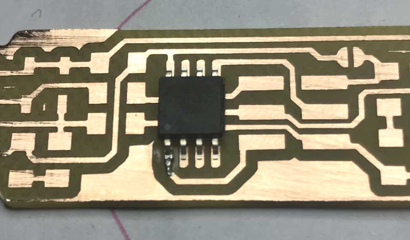
Next, press the soldering iron tip onto the pad and electronic component connection, simultaneously heating both. After a couple seconds, add solder. The solder will flow into and around well-heated connections. After adequate solder is flowed, remove the solder, then the iron. Good joins have a flat electronic component and shiny solder completely wrapping the connection. Bad connections can be reheated and fixed. Components can also be removed by reheating the connections and pulling the components from the board. When all the connections are soldered, remember to flow the first tack spot.
I started with the microcontroller because it is the most difficult to solder. Next I did the ISP which is also difficult.
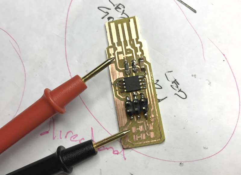
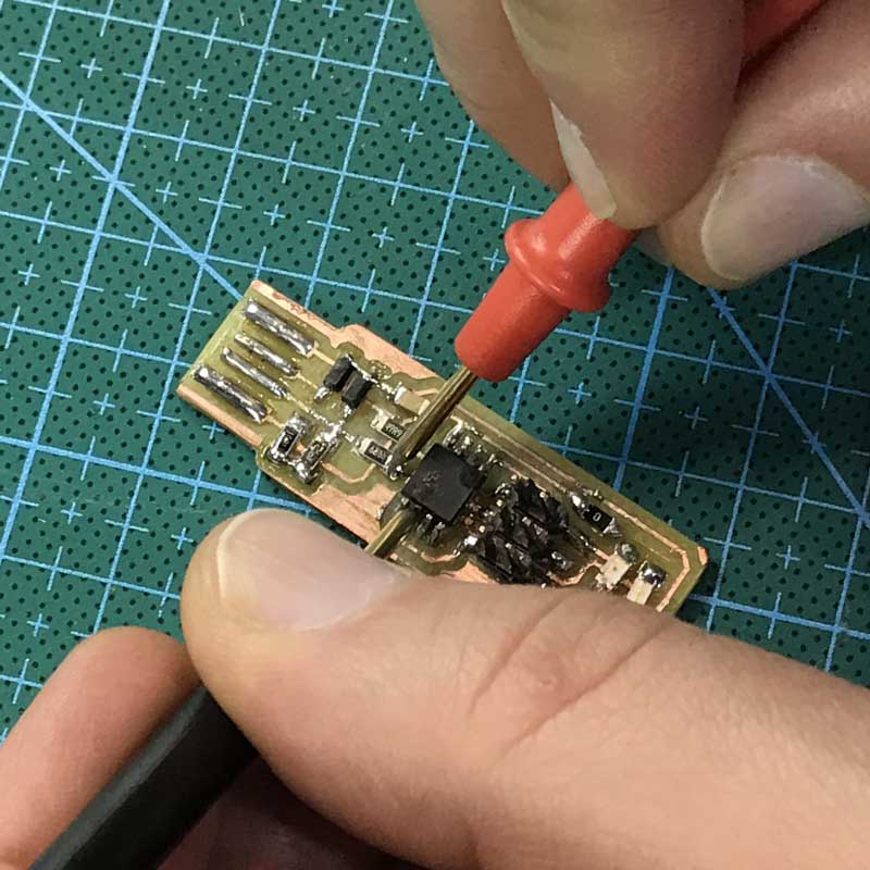
As I soldered components, I checked their connections with a multimeter. I put the multimeter to the check mode with sound. Follow the traces to check connectivity by pressing one wand to the connection point and the other further along the trace. Sound means connection. If that connection is undesired, check for extra solder. If no connection, re-flow solder at the intended connection.
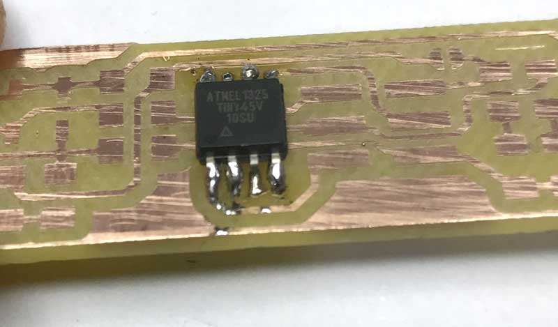
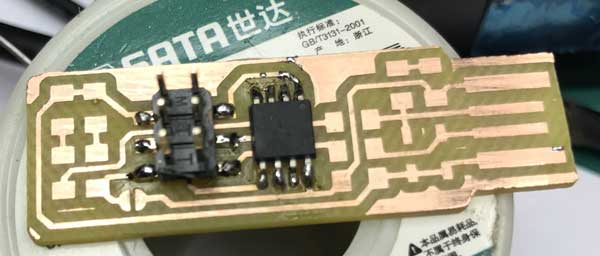
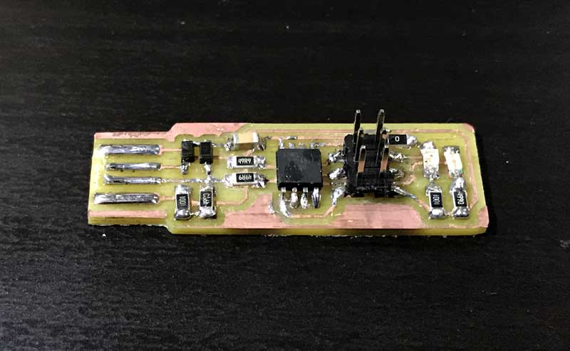
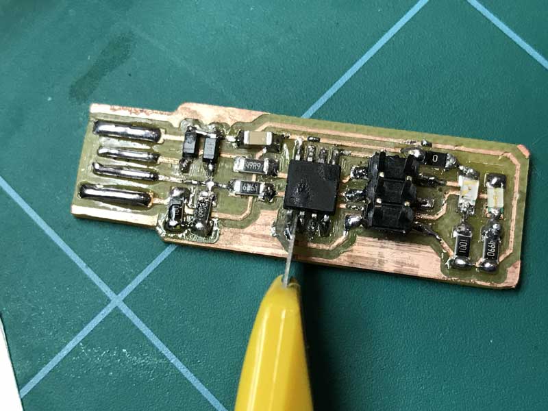
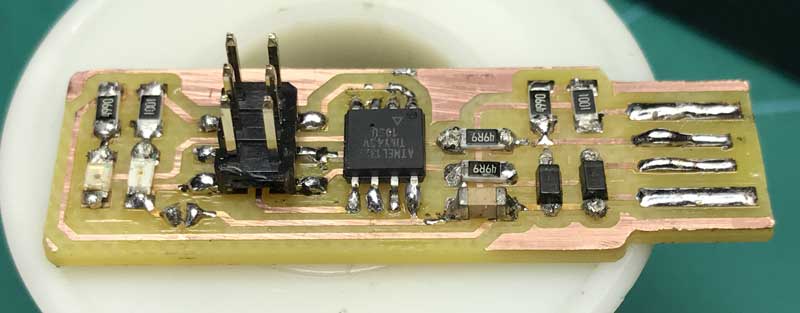
After about an hour of soldering and testing, I have what I hope will be an operational programmer. My second go around. I added solder along the USB leads to improve connectivity.
This is a photo of my first attempt, which I have yet to get operational. I do not hold out hope for this one...
I will post links to resources I have found helpful here.
Programming a programmer
An in-circuit serial programmer (ICSP) is capable of programming microcontrollers on various boards with only a universal serial bus (USB) cable and 6-pin insulation-displacement contact (IDC) to 6-pin IDC cable. The ICSP vastly simplifies what would otherwise be an expensive and laborious process across different chip types.
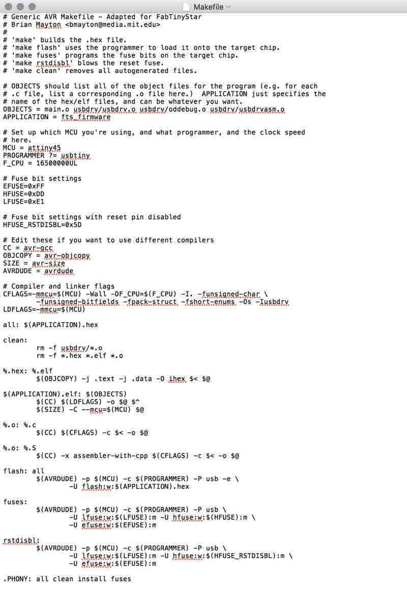
First I installed Crosspack on my mac. Crosspack is a development environment for AVR microcontrollers and necessary to give the terminal app capability for the upcoming task. Next, from the FabTinyStar page, I downloaded the firmware source code. I added a link here as well. You can open the Makefile with a neutral text editor, such as TextEdit or Brackets, applications common to this blog. It is important not to change Makefile's formatting or extension. Makefile displays setup information, commands, and some variables such as the MCU, PROGRAMMER, F_CPU (Clock cycles), which need to be set specific to your programmer. I am using a previously built FabISP to program my new programmer.
♻ FabTinyISP firmware source code ♻
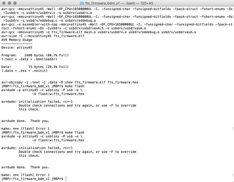
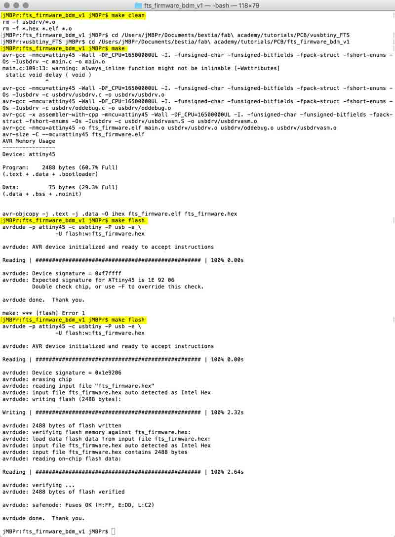
In terminal, cd (firmware location), then give the command "make". This will create some new files listed on the second to last line including fts_firmware.hex.
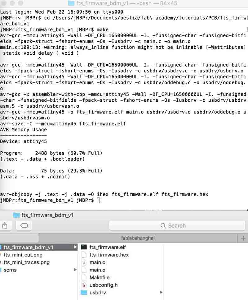
Now with the programmer connected to the newly made ICSP give the command "make flash".... and, fail. "make: *** [flash] Error 1". I could not work around this error in the terminal environment.
After the receiving Error 1, we checked the connections with a multimeter. Follow the traces to the connections and check that adjacent connections are not giving feedback. In this case, The first and second connection of the ATtiny45 were mistakingly bridged.
I severed the connection with a blade. Having these two spots connected would definitely cause problems. I will return to my mac with new hope.
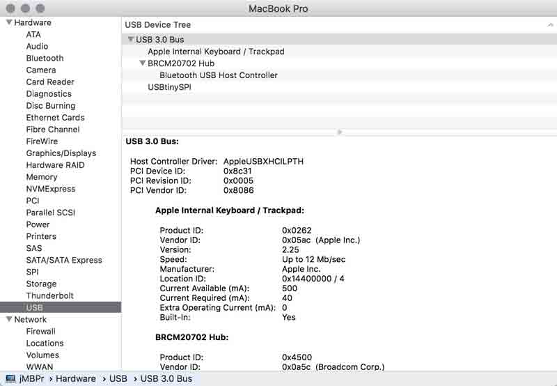
Unfortunately, I still am receiving the same error from my terminal. Unable to solve the problem, I have opted to start again from scratch. The following screenshot of my About this Mac > System Report shows a successfully connected FabISP. Not mine. Yet.
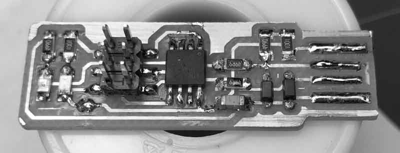
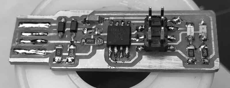
Update: I have a new board. This one is prettier. This one is pre-tested. I think this one will become a working programmer. First I cleaned out the firmware directory.
make clean
Then rebuild the computer language files...
make
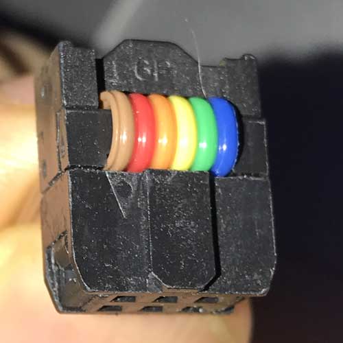
And send the instruction to the microcontroller. This will require a programmer connected to the 6 pin IDC with a programmer cable. Check the orientation of the programmer cable by aligning the marked connection spot iwth the dotted pin on the roadmap.
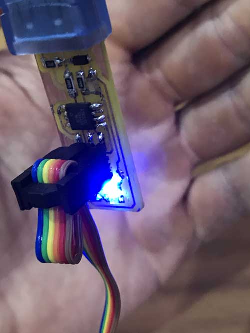
After the programmer is connected to your newly fabbed board, connect each to USB ports on your computer. At the very least, connect the programmer to your computer, the target board just needs some power. It can be connected to any USB port. When it is connected, the red diode should illuminate. If your fablab is like mine, blue diodes may have found their way into the red diode storage. In which case, someone was not careful with restocking!
When everything is linked, this command will tell the programmer to erase the microcontroller and program its flash memory with the contents of the hex file.
make flash
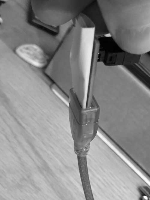
Error 1. This time however, the initialization succeeeded. "Expected signature for Attiny45 is IE 92 06". I searched Google for this specific error and found some tips written beyond my current scope of comprehension. Former FabAcademy student Yue Siew Chin had the same error and was able to resolve it: "The solution was very odd because it was after I heated up the chip area on the board a little with a hot gun or a hairdryer, it was able to load the program!" Okay, first I tried a low-tech fix: double-check the USB connection by adding a little paper underneath. Success!
Now make fuses, which will setup all the fuses except the one that disables the reset pin.
make fuses
Check the USB functionality by plugging the board into your computer and checking the device page for the new programmer. Here it is: USBtinySPI.
One last step: blow the reset fuse. First reset the the disable pin.
make rstdisbl
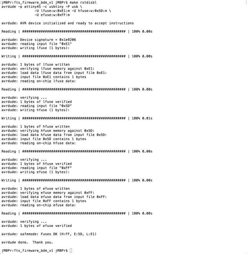
The reset disable command did not work when the programmer was plugged into an USB port on my computer. When I connected it to a port on an adjacent computer, the command worked.
Second, remove the bridge on the solder jumper. I did this by reheating the solder with a clean iron, which visually removed enough solder to disconnect the two sides. Then I double checked with a multimeter.
I will post links to resources I have found helpful here.
Jump : Index
J.travis Russett © 2017
 All the work contained within is licensed under a Creative Commons Attribution-NonCommercial-ShareAlike 4.0 International (CC BY-NC-SA 4.0) License
You may remix, tweak, and build upon my work non-commercially, as long as you credit me and license your new creations under the identical terms.