This weeks assignment falls involves three distinct stages;
1. Create boards
2. Stuff boards
3. Program the boards
In order to complete this initial phase, it is necessary to chose a board design from the list provided, download the design, and then mill out the traces using whatever machine option you have available.
I chose the “Brian” option.
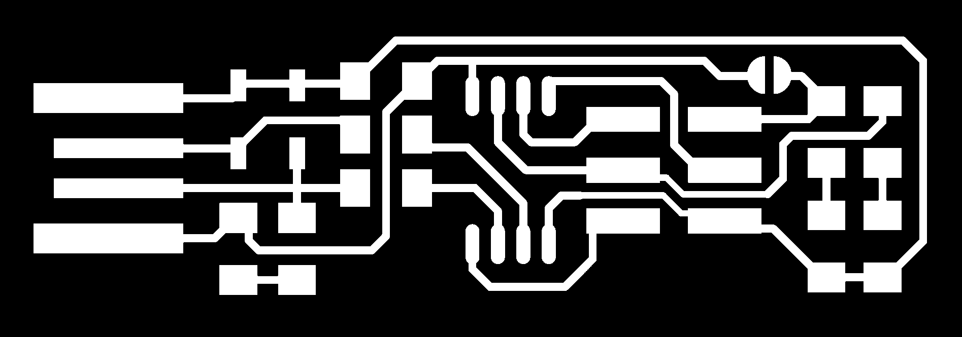
The 2 necessary files were downloaded in .png format.

Setting up the Modela
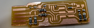
In our Lab, we will be using the Roland Modela MDX-20 desktop milling machine, via the older desktop Fab Modules. The traces file was processed first, and cut with the 1/64th” bit. This was a relatively quick process, taking around 20 minutes.
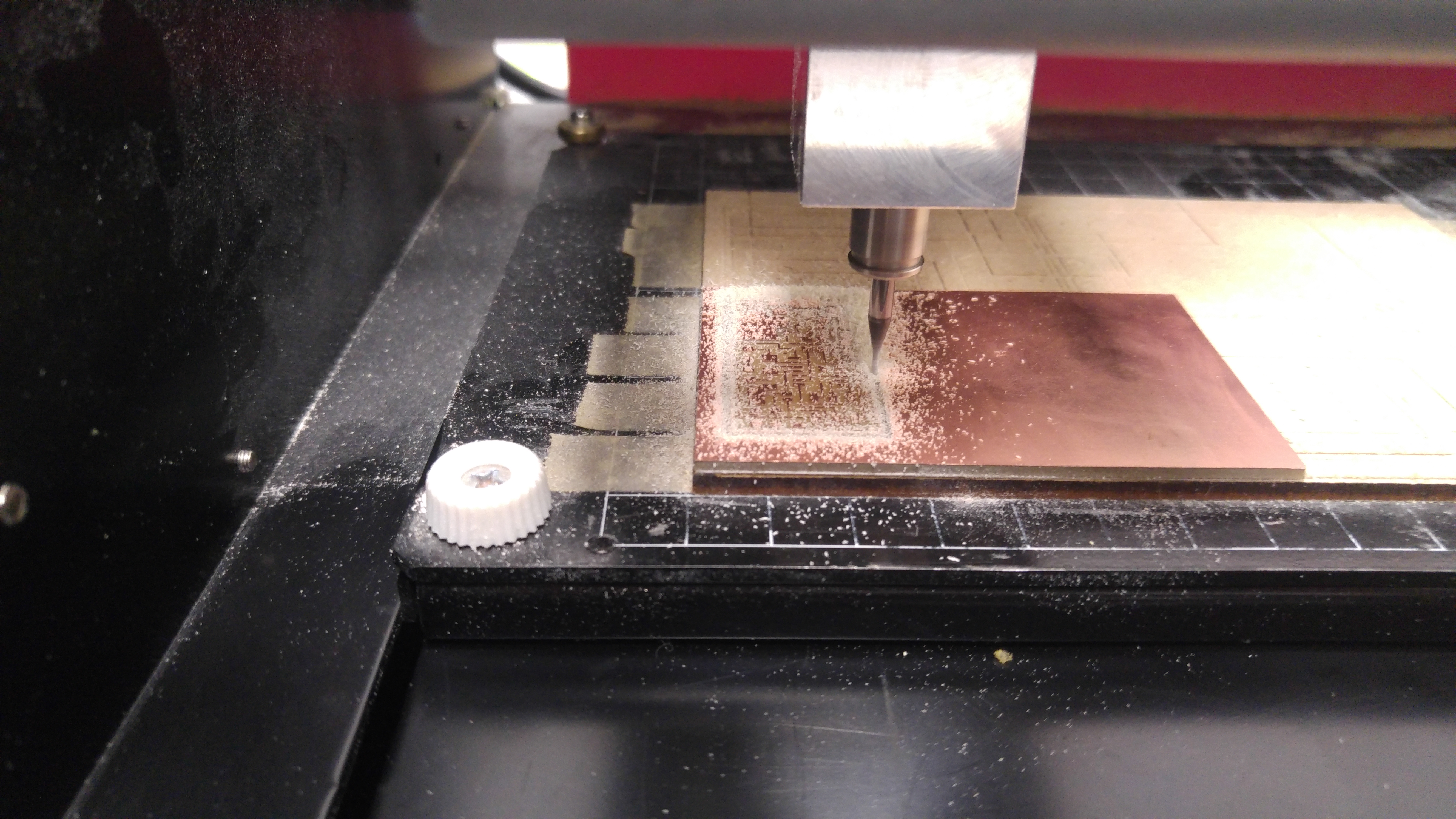
First thing needed was to select FR1 stock, and stick this on to the sacrificial board using double sided tape.
Now we need to ensure we have a 1/64th inch bit installed in the spindle. The bit can be inserted by losening the 2 allen bolts, then sliding the bit in. At this point the height of the bit is not critical, but it is best to only leave a small amount of the shank protruding.
Now you cn lowere the spindle closer to the bed. Normal practice is to only leave enough clearance in order to cut the traces. This will ensure less modulation at the tip of the bit, and therefore attaining better edges. Now, release the allen bolts, and gently lower the bit until it touches the top of the stock. We have now established Z zero.
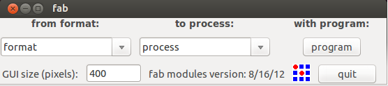
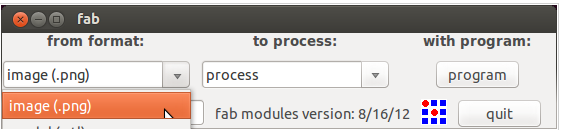
Next we need to convert the .png file into the correct format for interfacing with the Modela. This is the proprietary .rml file format. Conversion is very easily achieved if using Fab Modules. Simply load the .png file, having chosen .rml as the process.
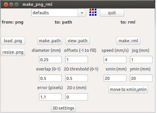
Next select mill traces from the drop down menu, and click on make.path. Now you can define the origin using the x min and y min controls. It is a good idea to double check the position by clicking on move to x min, y min. If this is correct, you can click on make .rml. Then you can send the file to the modela, and cutting will begin.
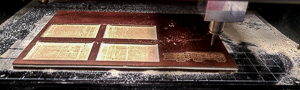
After cutting the traces, we need to change to the 1/32” bit so as to enable the cutting out of the board. Simply repeat the process using the cut boards option from the drop down menu.
Once the board has been cut, we can deburr by rubbing a solid edge over the surface. It is also a good idea to wash the board so as to leave a clean surface to accept solder.
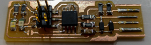
Soldering
The next step is to gather up the components, and solder them to the board. From the instructions the components needed were listed as
1x ATtiny45 or ATtiny85
2x 1kΩ resistors
2x 499Ω resistors
2x 49Ω resistors
2x 3.3v zener diodes
1x red LED
1x green LED
1x 100nF capacitor
1x 2x3 pin header.
 I decided to work from the centre outwards in order to maintain good access with the iron. I have soldered cables before, but not boards like this, so we cut a few extra boards for practice before moving onto the proper board. This was a good strategy, and within a reasonable amount of time, i was able to increase the accuracy, and predict the action of the iron a lot more.
First off, i gathered the components and laid them out on the desk in order to aid speed when locating.
Next, i tinned one of the pads for each component. This was done by placing the tip of the soldering iron on the pad, allowing it to heat for a second or two, then applying just a small amount of solder on the pad until it flowed nicely. The iron can now be removed, leaving a nice shiny dome of solder.
Now, using tweezers the component is laid across the pads and the solder heated until it flows. Now you can pull back the tweezers and the component will be fixed to the board. The opposite end of the component can now be soldered by holding the soldering iron onto the leg and introducing solder until you can see it flow on and under the pad. Hold the iron for another second or 2 until you can see the solder flow, then remove. This should leave a tidy solder joint.
Some of the components, in particular the diodes are polarised and therefore need to be set on the board in the right orientation. It is marked on the schematics and also on the component, but care is needed due to the size of the smd components. If unsure, you can use a meter in diode mode in order to identify the positive leg.
This is repeated for each component until you are finished.
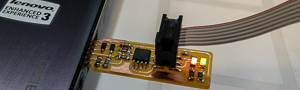
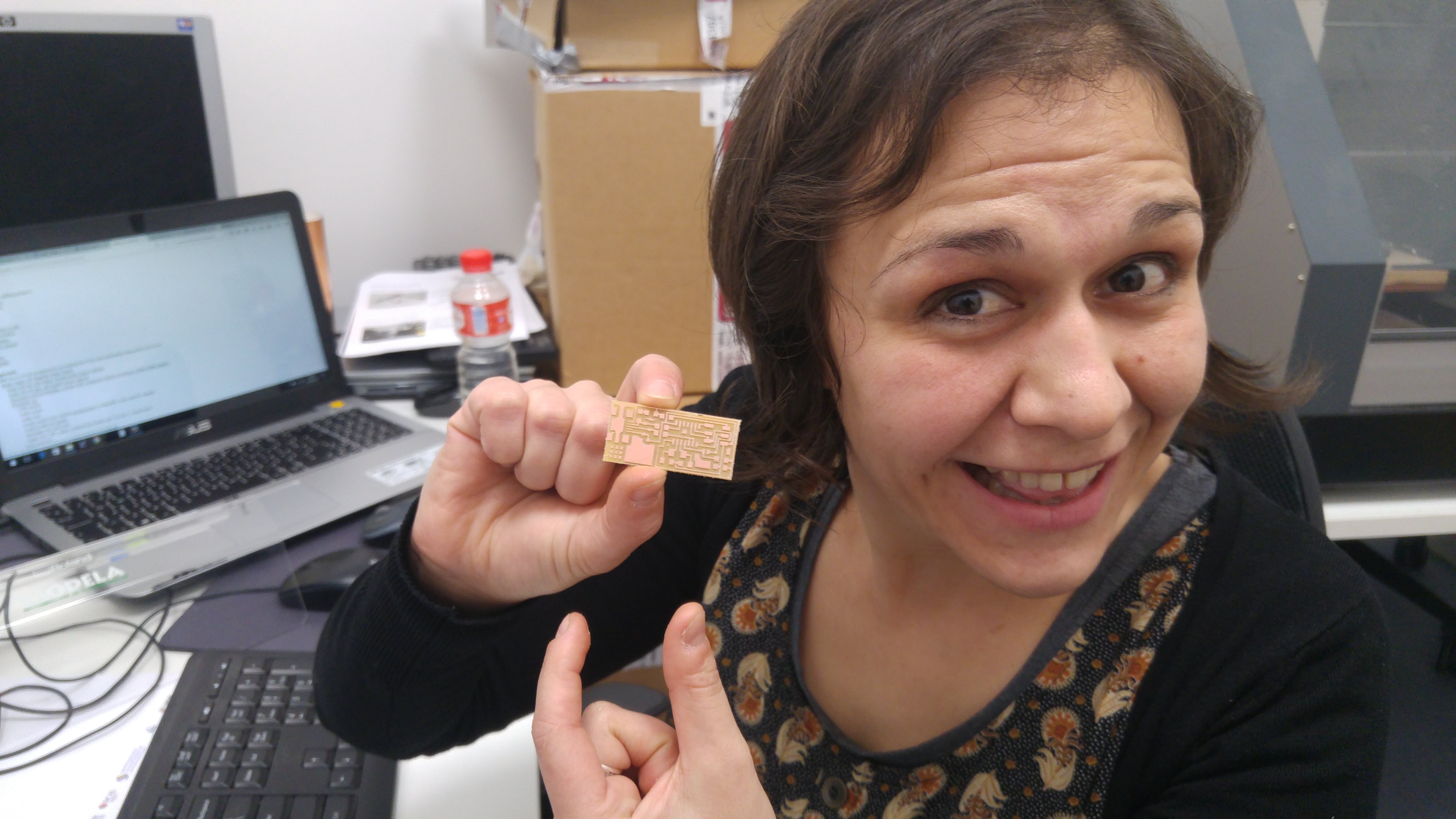
The finished board looks like this.
Observations
On first attempt, i was using lead free solder. Whilst it was ok in operation, when I switched to lead solder it noticed that it heated better, flowed better, and created more shiny, tidy joints. Using in small amounts like this is probably ok, so i think i will use leaded solder in future.
Also on first attempt, i was tinning 1 pad then applying component, then moving to next. On the second attempt, I tinned 1 pad of each pair in one pass. This sped up the creation of the board quite considerably.
Once the board had been stuffed, the next process was to progam the chip sa that it could function as an isp. There were a few steps to this.
Windows Issues
We started the programming phase using windows 10. We followed all of the sreps in the tutorial, but still could not get the system yo work. We could not even get the computer to recognise the avrisp mk11. This took up a few hours in total, with all sorts of attempts to overcome the issues, but as soon as you solved one issue, another one presented itself.
So a decision was taken to abandon windows.
With the ongoing disaster with windows, i decided to drive home and return with a laptop that runs on ubuntu 16.0.4. The instructions in the tutorial for this seemed a lot more straightforward.
First the command sudo apt install avrdude gcc-avr avr-libc make was run from terminal.
Next, the firmware fts_firmware_bdm_v1 was downloaded and unzipped .
The next step was to change directory to that of the folder that contained the firmware.
Running 'make' in the terminal successfully created the fts_firmware.hex. file.
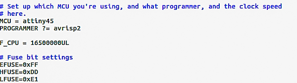
Next step was to edit the Makefile so as to suit our current commercial isp programmer - and AVRISP Mk11.
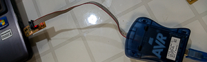 It was also necessary to have the usb side of the new board inserted into a usb port (preferably usb2) so as to provide power. To be honest, the design of the board is a little unstable when plugged into a usb port. Getting a strong relaible mesh between the board and the port was not as easy as it should be. I will need to investigate the best material to stick onto the back of the board to provide a much more snug fit in future.
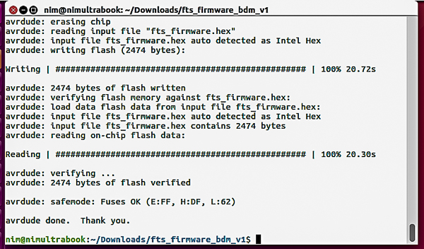
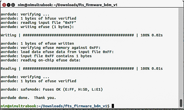
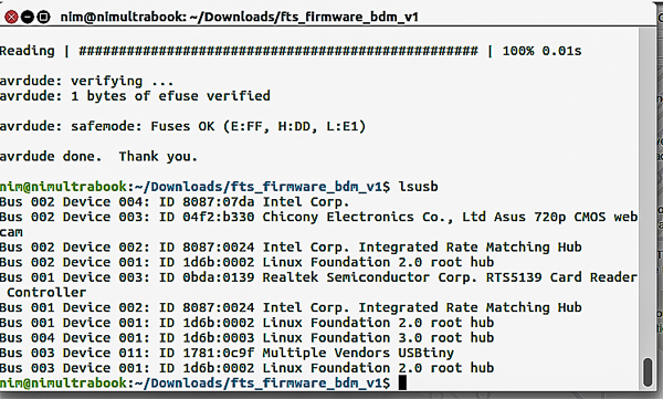 Finally rstdisbl command was executed, and the solder was removed from the jumper. The board is now complete.