Electronics Design
Redraw the echo hello-world board, add (at least) a button and LED (with current-limiting resistor), check the design rules, make it.
Learning outcomes:
Further Evidence:
- Shown your process using words/images/screenshots
- Explained problems and how you fixed them, including how you worked with design rules for milling
- Included original design files (Eagle, jpg, rml)
Getting Started
This week’s assignment started well. I am not a pro at electronics, but I have been teaching High School Physics for years now, so basic circuit diagrams are a happy place for me to get started. While the traces shown on the ‘Hello World’ board are not exactly schematics, tracking them is essentially the same skillset. I have never used Kokapelli, but it looked interesting. Even just reading the schematic for the original hello world board solidified that I need to find a computer that I can sacrifice to the Linux gods. Access to that platform will be a great way to expand my horizons. I have had Linux machines in the past (college days), but not presently.

Software
I have designed my version of the hello world board in Eagle CAD, now an AutoDesk product. I had played with Eagle CAD many years ago for a college class, when its logo was still the red eagle. Since I am working on a Windows computer, it seemed to make the most sense. Also, I have some small level of acquaintance with the software. It took a bit of work, but I got reoriented with the Eagle interface to get designing. I greatly appreciated the fab.lbr library, as I vaguely remembered that selecting the correct parts from Eagle’s many libraries was often the most difficult part of its use. I also made some use of the supply1 library in Eagle, just to reference things like ground and Vcc voltages for the circuit schematic.
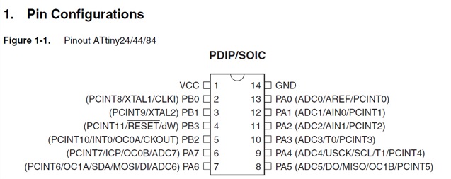
The first step is to get ready to design the schematic for my hello world board. It seemed that I could use the example Hello World board to guide my re-development of the schematic. I also looked up the datasheets for the ATtiny44 so that I could properly connect the Integrated Circuit pins to the needed inputs and outputs, even though this was redundant (since the example schematic is so detailed). It was part of the assignment and I figured it would be good to give the Atmel datasheet a once over, just for reference, anyway.
Design Process
So design begins… I started my own version of the schematic, making use of the supply and ground components (from supply1) to try and keep the lines and wires as simple as possible. I see a lot of schematics made by high school students, and I appreciate how much easier they are to read when simple and clean. First I placed all of the components in positions that seemed to make sense around the schematic area. Once those are present, it is easy to trace out all of the linkages shown in the example board. You simply need to place the parts from the libraries in Eagle, and connect them with the friendly green lines. Analog circuitry basics.
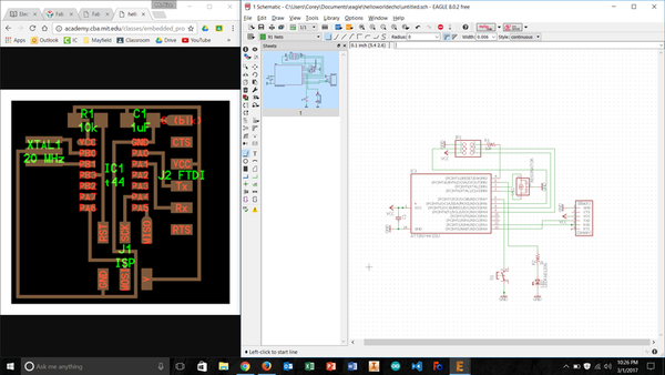
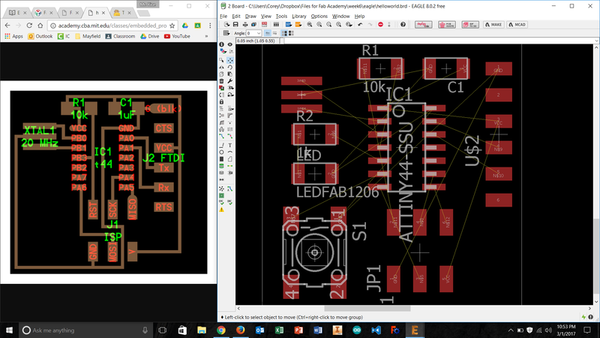
The schematic went fairly well, but that was the easy part. Then I used Eagle to export the schematic to a board. The actual exporting went well, but this is where my skills started to hiccup. Eagle dumps all of the parts onto the board in an unorganized pile, connected with (appropriately named) ‘ratsnest’ lines. The GUI interface is frustrating - the click points don't immediately make sense. I had to constantly zoom in and out to grab the right parts and move them around without having the ratsnest lines switch over to traces. Frustrating, but not impossible. Once the parts were reasonably in place around the board, I was excited to try the autoroute feature. It is just satisfying to watch a computer solve your problems for you.
Working Through the Details
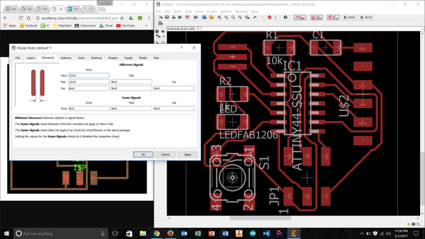
Alas, it was not as easy as the click of a button. The autoroute feature was configured for a two-layer board by default. The results included top and bottom traces, along with vias. So I elected to do some research to configure Eagle for autorouting in only the top layer of copper. Once established, I used the ripup command (which my previous research had found) to remove the top and bottom traces I had gotten. Then I restarted the autoroute process. It seemed to generally work, but some components weren’t connected, so I tried to evaluate why.
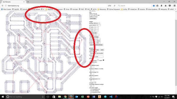
After a bit of looking and research, I realized I had not properly configured the build parameters for my traces, and so they were all too large of traces and clearances to be useful. I found this menu within Eagle, guessed at what reasonable settings might be, used 'ripup;' and then tried again. These traces were better, but I still needed to change a few configurations. A few more trips through this revision process, and I had something. Once this process was complete within Eagle, I exported the results to a png file at 1000dpi and uploaded it to fabmodules.org to generate toolpaths. The first iteration did not have enough clearance between the traces to fully separate them everywhere it was needed. This meant I was back to the iterative design cycle to space the traces out a little more.
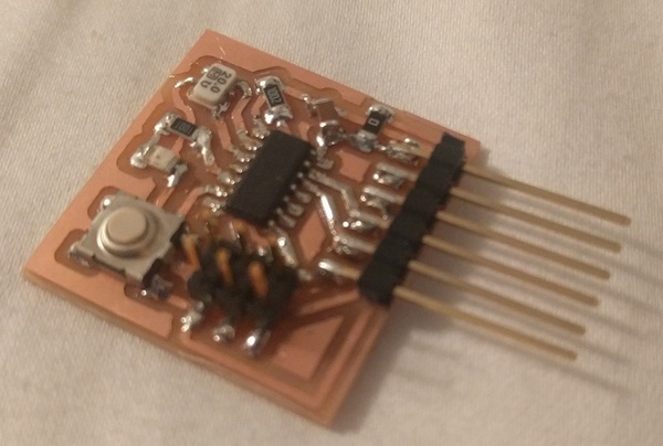
By Friday afternoon I had a milled board that I could quickly clean up and solder components onto. Before I finished for the day, I plugged the part into the FTDI cable I had been sent by my instructor, excited to see how it would go. It didn’t. I was confident that it was simply a consequence of having not uploaded code to the ATtiny44, until I took a second look at the board. In all of my iterative design, I must have lost track of the trace connections and didn’t notice that Vcc from my FTDI plug was not connected by a trace to the Vcc pin of the IC. Stupid mistake. It could wait until I was next in the lab.
Saturday I received an ominous phone call. My grandmother, who had been growing unwell from dementia/ alzheimer’s disease, was projected to only have hours to live. I dropped everything and drove home. She passed that evening and all of my remaining work for the week was delayed until after the funeral services. Family comes first, in how I choose to navigate the world.
A new week, and we are back to Electronics Design. I went back through the iterative design process and made some changes to the board so that all of the needed connections are present. This included tilting the voltage regulator cap and pull-up resistor for the reset pin. I also added a zero ohm resistor to bridge over a trace. It may have been possible to change the parameters for my traces so that they would all fit together better, but I liked having the clearances set for 16mil and the traces at 12mil. Most importantly, it worked.


======================= UPDATE ===============================
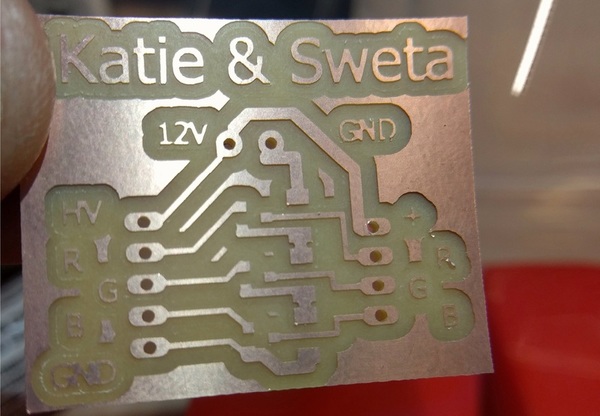
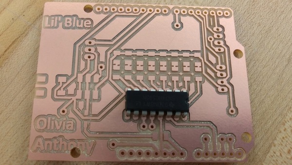
I later programmed the board described above, and it worked nicely. I also converted an old, near lifeless, computer to an Ubuntu desktop. I also used these skills to help a few students build better circuits for projects, or help them design their own circuits as shown below by these two examples:
Below I will summarize the total workflow that can take you from thinking about a circuit, to having one milled by a Roland MDX-40A and soldered together.
- Open Eagle CAD and make sure you have a ‘Project’ to work in, and a schematic file to start your design.
- Make sure that you have all of the parts you need in the libraries loaded on your computer. If you think the fab.lbr is missing any parts you need: 1) search your libraries, 2) download more libraries, or 3) make your own parts. By the end of the course, I had done all three of these alternative methods.
- Place your components into the schematic and try to arrange them in a sensible order.
- Connect all parts, as appropriate with the green trace lines.
- Once all schematic connections are made, press the magical ‘convert to board’ button and watch your components’s footprints show up in a new file with a bunch of yellow ratsnest lines.
- Move the footprints around until you think all connections can be made nicely. [I always designed for a single sided board, since this is what is easiest to mill and the only stock I had.]
- Build your traces, either by hand, autoroute or both! Keep in mind the limits of your mill at this stage – this means you need to change the Edit >> Design Rules… I had to change the ‘Clearances’ all to 16mil and the ‘Size’ to 12mil. Larger traces should be drawn for higher current, but are harder to autoroute around. Also, you will likely want to turn all board layers to ‘N/A’ in the autoroute wizard, unless they are the top layer (to avoid multilayer autorouting).
- So, the first pass at traces didn’t give you 100% completion? It almost never does. You can either hit ‘CTRL + Z’ or enter ‘ripup;’ in the command line to start again. At this point, you will need to try and move or rotate your parts to get closer to the 100% routed state.
- Success! Your traces are all perfect, and everyone is happy. :) Double check everything, just to make sure you didn’t do it wrong…
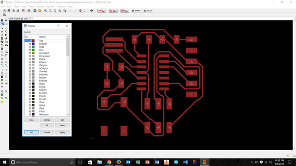
- Export the project as an image. It is good to export the project three ways:
- The ‘full view’ with all of the layers visible, at 1000dpi
- Just the ‘traces’ and pads’ layers, at 1000dpi and monochrome
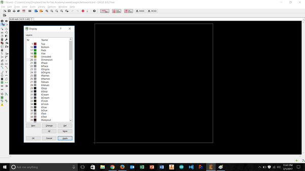
- Just the ‘dimension’ and (if needed) ‘holes’ layers, at 1000dpi and monochrome
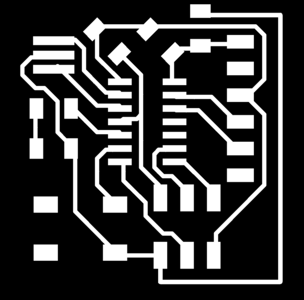
- Edit the images in MS paint to remove any junk (text, annotations, etc.) that you don’t want to cut on the mill. This is important to do in a simple pixel-for-pixel editor such as paint, since the pixels are what actually map out your cuts. A few things to note:
- Clean your ‘traces’ image completely, so that it looks like what you want your finished product to be.
- Change the ‘dimensions’ image, so that the board area is filled with white. You may also need to add thin black lines around the edges, if Fab Modules (in a few steps) isn’t able to fit tooling all the way around your edges.
- Save the ‘traces’ image as a duplicate, and use the holes depicted there for any through-hole components to design an image that divulges those holes position on your board.
- Use Fab Modules to generate the toolpaths for your mill. This will involve uploading the images you just made, and selecting the correct processes and parameters. I usually cut my traces at the default setting, with the 1/64 mill bit and the through holes and outline as two processes with the 1/32 mill bit and the settings for a little less depth than needed, so I don’t cut my waste board in the mill. I cut these holes all the way through later. Occasionally, would adjust the mill bit width settings to make the toolpaths better suited to what I ultimately wanted.
- Place the copper-clad board in the mill with double-sided tape, set up all three axes for operation, and run the toolpaths in the most sensible order.
- Remove the newly milled board, free it from the stock, clean out any holes that need it, and sand it down to take off any spurious copper.
- Solder on the components, paying special attention to the orientation of the parts on the board.
- You’re done! Celebrate by doing a dance and give some high-fives! Then program your board…
You can see all images (used and unused) from this week's work HERE.