Invoked - it reported missing component library.
Installed components library.
sudo pacman -S kicad-library.
Pondered the net about various linux based e-cad software.
Decided on kicad.
Also, gone through the 286-page ATtiny24A/44A/84A data sheet.
Spent time designing with the help of the KiCaD official help dcoument "Getting Started in KiCad"
Learned to: Create schematic-Add component - create component library if not existing - annotate components -
perform rule check - add foot prints and associate - run CvPCB - Generate Netlist - Generate BOM
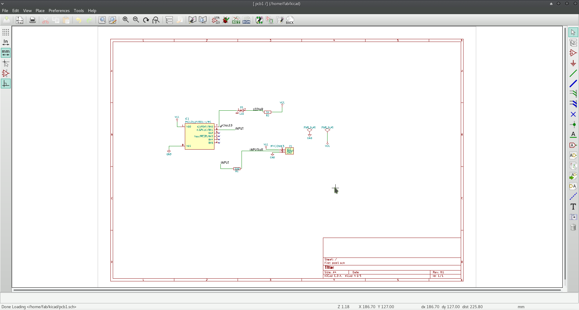
Using Eeschema drawn the schematic of the tutorial circuit provided by KiCad.
http://archive.fabacademy.org/2016/fablabhrw/students/165/fablab-inventory_kicad/fablab-inventory.zip
http://archive.fabacademy.org/2016/fablabhrw/students/165/fablab-inventory_kicad/fablab-noninventory.zip
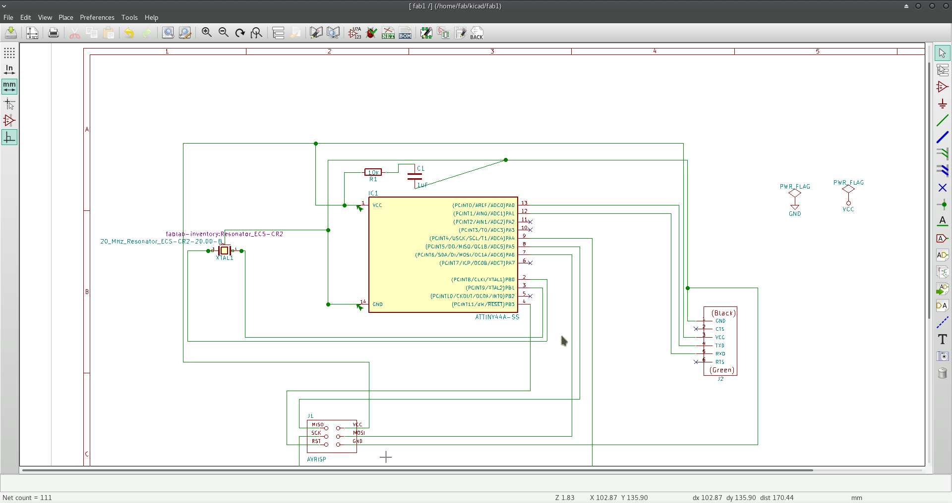
As of now the power sources are not shown and hence related warning are there. To investigate.
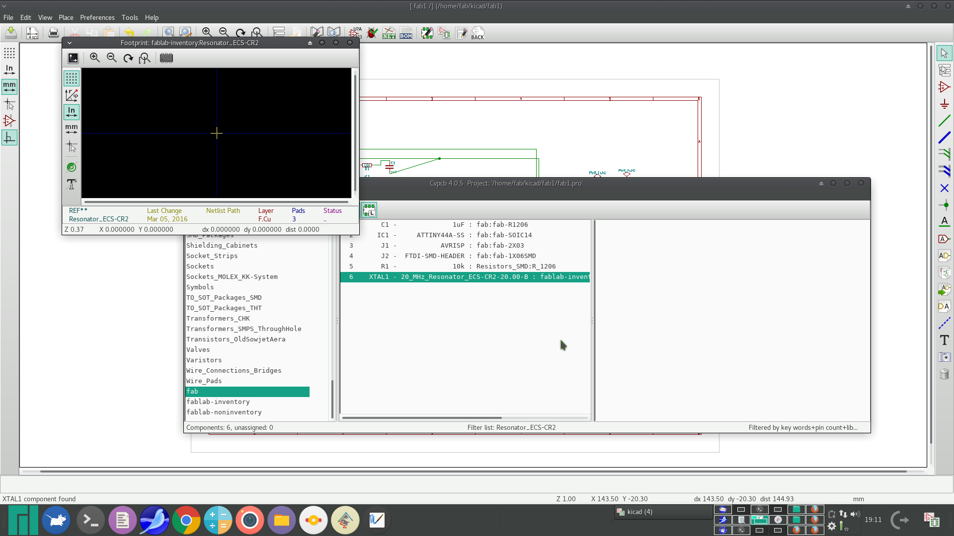
Run Cvpcb.
Components are then selected from the middle column of the Cvpcb window.
To decide on the footprints the following documents are referred
(1) The inventory list of the lab
(2) The specs of the component as obtained from the links of the fabacademy electronics design assignment page
Bill of material is generated from eeschema. This plugin is added for that - /usr/lib/kicad/plugins/bom2csv.xsl
set the design rules
read the net list
errors of undefined footprints
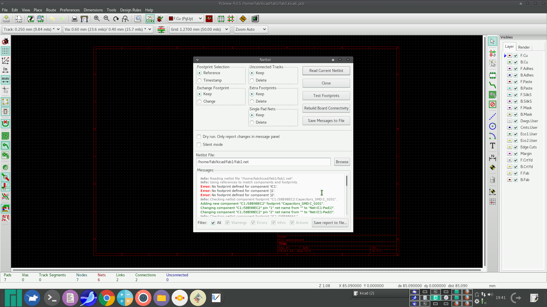
fab library path was not properly set.
done it.
net list reading succeeded.
layout is rearranging
"J2","FTDI-SMD-HEADER","fab:fab-1X06SMD",""
to
"J2","FTDI-SMD-HEADER","Connectors_Molex:Molex_NanoFit_1x06x2.50mm_Straight",""
to match the connector in the lab. Also as per instruction from tyhe instructor some other slight changes are made with foorprints selctions.
The old and new values are shoen side by side here
| Old footprint |
New footprint |
| Reference, Value, Footprint,
Datasheet "IC1","ATTINY44A-SS","fab:fab-SOIC14","" "R1","10k","Resistors_SMD:R_1206","" "C1","1uF","fab:fab-R1206","" "J1","AVRISP","fab:fab-2X03","" "XTAL1","20_MHz_Resonator_ECS-CR2-20.00-B","fablab-inventory:Resonator_ECS-CR2","" "J2","FTDI-SMD-HEADER","fab:fab-1X06SMD","" |
Reference, Value, Footprint,
Datasheet "IC1","ATTINY44A-SS","fab:fab-SOIC14","" "R1","10k","Resistors_SMD:R_1206_HandSoldering","" "C1","1uF","fab:fab-R1206W","" "J1","AVRISP","fab:fab-2X03SMD","" "XTAL1","20_MHz_Resonator_ECS-CR2-20.00-B","fablab-inventory:Resonator_ECS-CR2","" "J2","FTDI-SMD-HEADER","Connectors_Molex:Molex_NanoFit_1x06x2.50mm_Straight","" |
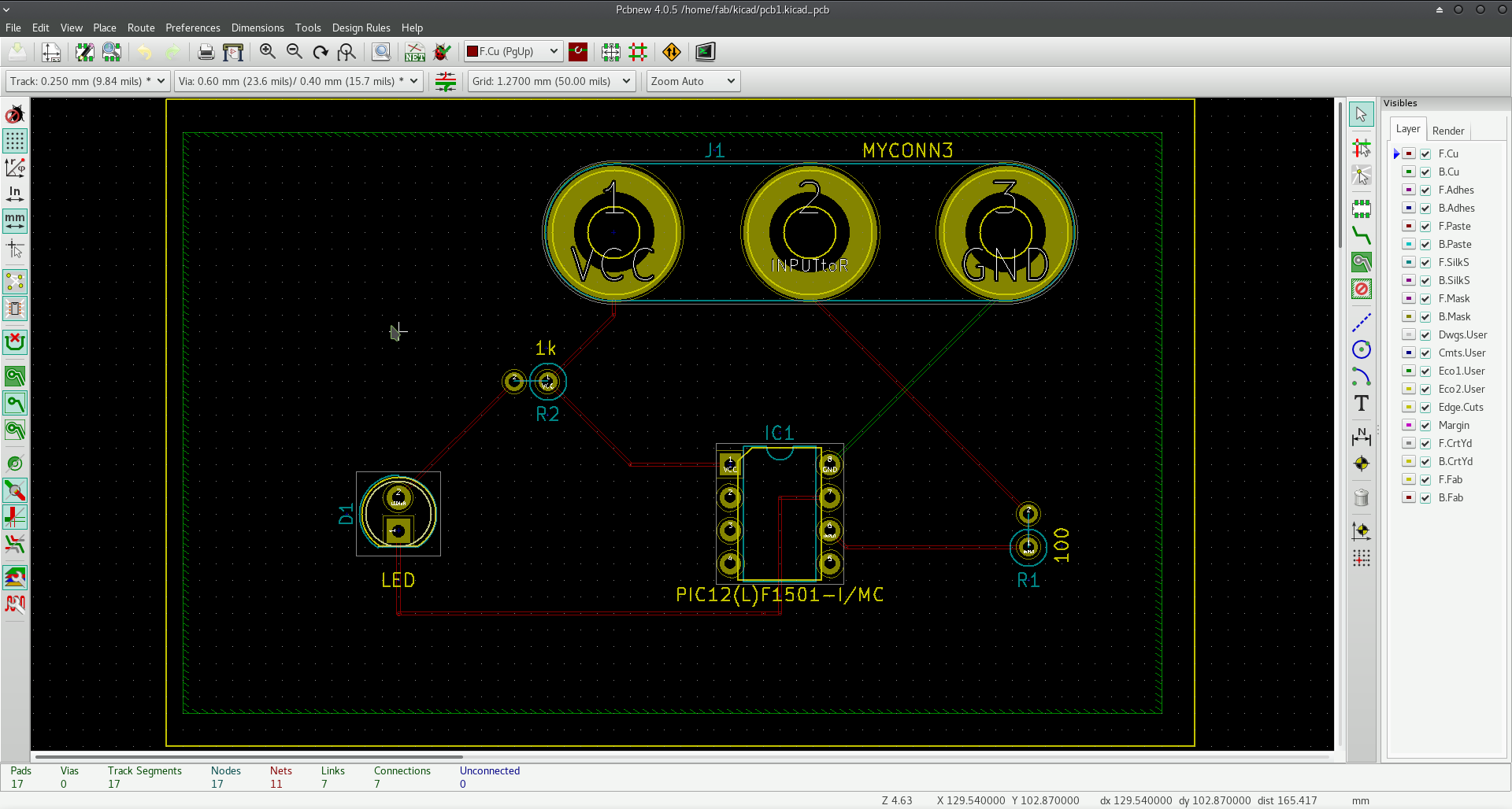
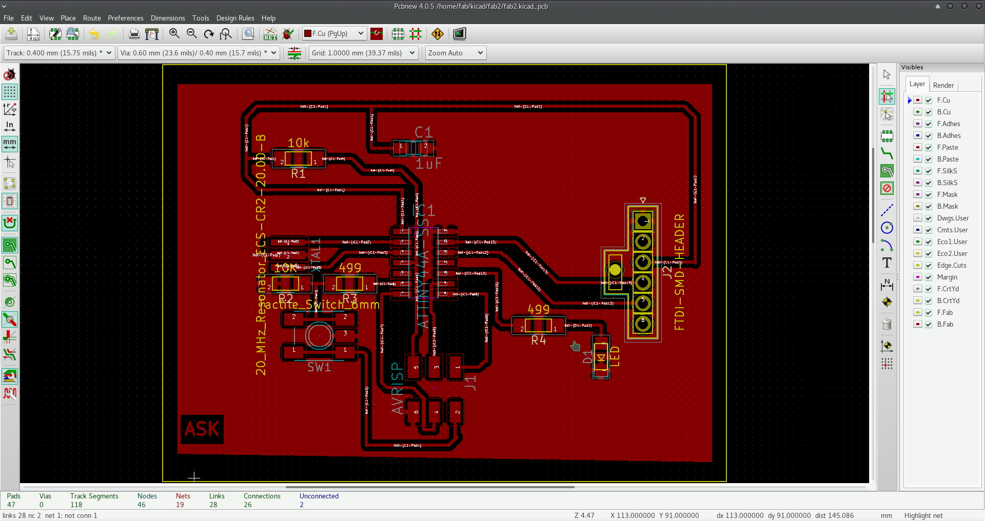
Varying the grid resolution was helpful while drawing the tracks underneath the IC and J1 connector.
Here is the layout.
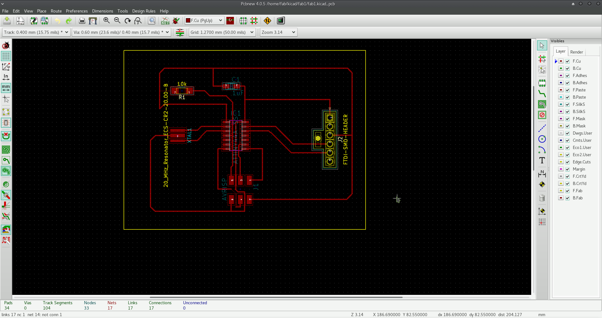
This is not drawn to mill. Now the LED and push button will be added as per the assignment.
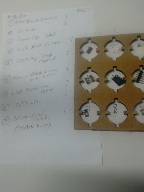
Identified components to be added:
1. Push Button switch: SWITCH TACTILE SPST-NO 0.05A 24V
2. Green LED: LED GREEN CLEAR 1206 SMD
Both are checked to be available with the lab inventory.
And, read about the port A and port B pins of ATtiny44A IC. We have PB2, PA2, PA3, and PA7 as unused in the given hello world ckt.
And looking at the ckt layout decided to connect the button on the left side of the IC and the LED on the right side.
So, let us connect the button to PA7 and LED to PA3.
Gone through the data sheet of the switch & LED
Switch: Observed that its current range is 1 to 50 mA and voltage range is 3 to 24 VDC.
LED: Around 2V to glow the LED at 20 mA.

The Button may be connected with a pull-down resistor and a safety serial resistor.
PA7 may be given 10mA current. So, 5V/10mA=500ohm resistor in series, and a 10K pull down resistor may be tried.
To light it around 20 mA current may be good.
Typical pin out voltage is taken as 4V.
Hence 4V/20mA = 220 ohm resistor in series
Searched the google for fab archive whether my decision is in the right direction.
But, it landed on a 2017 student itself!
Checked the page of Emanuele Goldoni.
He has documented things very well and I could see that his design and decision almost matched with mine.
I just pointed him about a broken link, and we had a few mails exchanged.
With these Button and LED inputs the circuit is modified.
While completing the schematic struck with the situation that there is one VCC wire which cannot be connected on a 2D plane (one side PCB design).
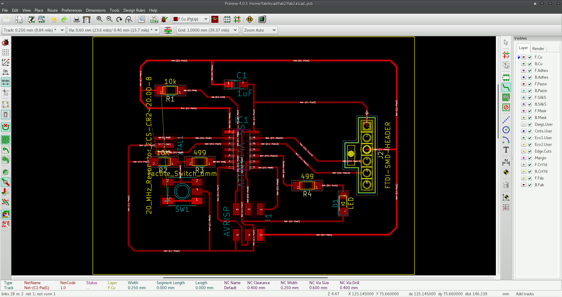
Then my colleague Suhail Pakkada suggested me to make the background fill with VCC. Instead I chose to fill it with GND and reduce the net of wires.
When 3D viewed, only PCB was viewable - no components, may be because the 3D views of the components are not there in the library.
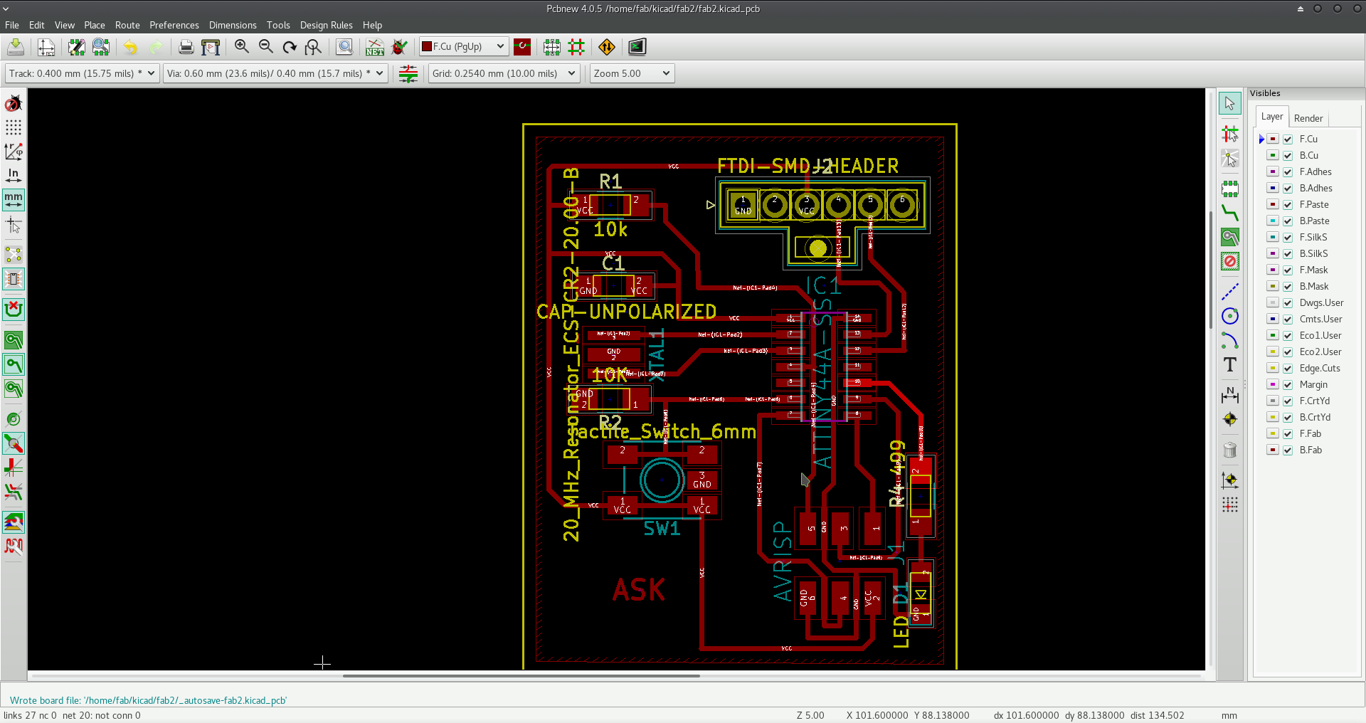
During this process two disconnected GND copper lanes were created. Hence GND tracks were connected again after some rearrangement of tracks. Now, no DRC error. No disconnected components/ areas. The board now looks like this.
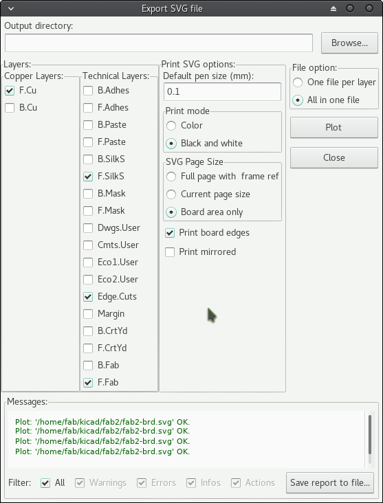
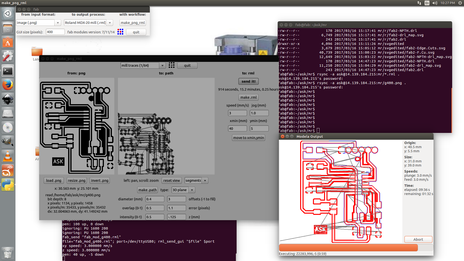
(1) Since I have connected the ground to the copper I need to have copper background on the plate. So inversion of the colours are needed in SVG. Took time to solve the issue. Finally come across the option provided by fabmodules.org.
I decided to install the modules in my system - proceeded as per the documentation.
cd
git clone https://github.com/FabModules/fabmodules-html5.git fabmodules
cd fabmodules
npm installnpm start
[1] 3259
[fab@ask fabmodules]$
> fabmodules-html5@1.0.0 start /home/fab/fabmodules
> PATH=./mod_server/:$PATH node ./mod_server/mod_server.js
listening for connections from 127.0.0.1 on 12345.
(2) The plot generation from KiCaD gives a lot of options. I have spent time trying to understand its implications on the milling process - yet to completely grasp it. For example there are options of multiple or single file generations. How shall the milling machine handle them?
(1) Substrate: The support layer - non conductive.
(2) Copper layer: Obviously the conducting layer
(3) Soldermask: Green or purple insulating thin layer, to prevent the expose of the copper layer.
(4) Silkscreen: Above soldermask. White normally. To write PCB indications.
So, concluded that since we may now omit the silkscreen layer and the bottom layer B.Cu as it is a single side PCB.
Also unchecked Plot foot print values and references. Retained the exclude pcb layer checked.
Default line width is changed from .1 to .4
for drill file default unit changed to mm from inches
drill file and drill map file are created. (in mill.all directory)
Then negative plot is selected and the results are stored in another directory - mill.all.rev. Now I see that the mask inverted (and required) plot is ready.
No, somehow something messed up!
Not convinced with the conclusion. So tried again. But, the problem is svg files when resized using inkscape are met with with svg path not found errors. Tried many options and unsuccessful. Installed web based fab modules and it seems not communicating with the plotter.
Frustrating? Not entirely yes, not entirely no!!
Then a png image is created and printed.
But due to the lower resolution of the image the tracks were coarse and at placed got merged.
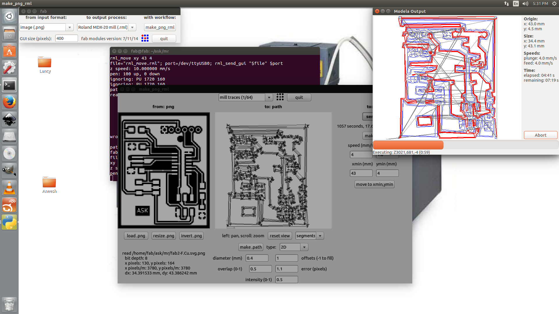
Now, high resolution (900dpi) png images are created.
But, some areas where not drilled enough.
Tried again many options and again printed a PNG image this time with the bits adjusted a few times with the help of the instructor.
Now the PCB is printed, but the holes are to be drilled and edge cut to be performed. Again some tedious task, as alignment was an issue as the the operations are based on two different PNG images. After doing a few rounds of drilling on the air the positions was readjusted with x, and y coordinates 1mm each behind the settings for the copper layout milling.
Still, the holes have not reached the other side and at two sides the edge cuts are not deep enough.
Checked the connectivity of various points and it is okay. Holes were deepened enough with hand drill. and edge cuttings are completed using scroll saw.
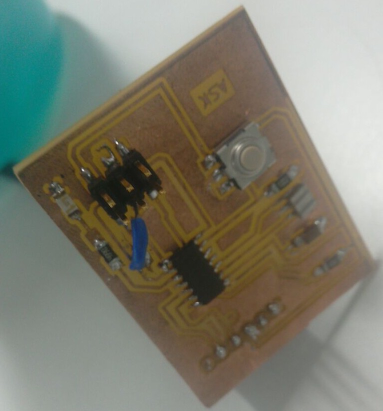
Then the circuit is connected to the PC via FTDI cable and checked whether it is sensed.
It seems okay.
Then without much care connected the fab - isp to the board - may not be with the right connector polarity. After some time it was detected that the fab-isp IC is heated up. Connection detached and on testing it seems that the fab-isp is damaged!! Connected the fab-isp to the USB port and checked.
So seems damaged. To inspect further later.
Any way, the ckt is connected to the 'damaged' fab-isp and issued the programming instruction.
So no use.
Hence by using another ISP the circuit is checked and programmed.
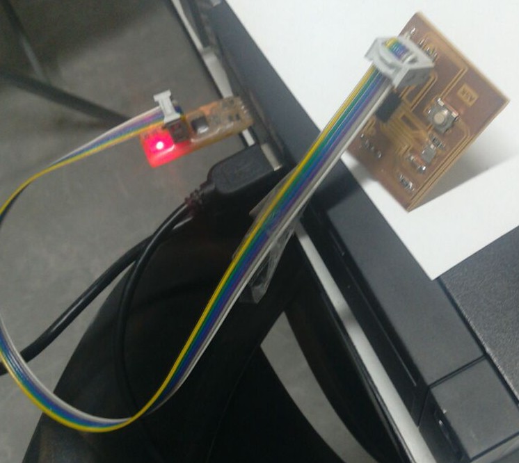
The ckt then detached from the fab-isp and connected to the USB port of the PC via FTDI cable.
At that time to ensure polarity a marking is made on the rear side of the PCB.
For polarity - FTDI cable pin one is coloured black.
But the circuit seems behaving intermittently, with LED on it staying ON at times.
And also the response to the send and receive communication with the IC was intermittent.
Rechecked the connectivity and re soldered some suspected points. Now seems okay.
To know about the ftdi modules
[[fab@ask ed]$ lsmod |grep ftdi
ftdi_sio 53248 0
usbserial 40960 1 ftdi_sio
usbcore 208896 9 usbhid,usb_storage,ehci_hcd,ftdi_sio,usbserial,xhci_pci,uas,xhci_hcd,ehci_pci
The suggestions in this link helped to ensure that the FTDI is properly interfaced with the PC. http://www.sealevel.com/support/article/AA-00524/0/How-to-configure-USB-serial-adapters-in-Linux.html
To know the current USB serial devices connected:
[fab@ask ed]$ ls -al /dev/ttyUSB*
crw-rw---- 1 root uucp 188, 0 Mar 20 18:51 /dev/ttyUSB0
To ensure that there is a process running to communicate with ttyUSB
[fab@ask ed]$ cat /proc/devices | grep -i "ttyUSB"
188 ttyUSB
For further details:
[fab@ask ed]$ sudo cat /proc/tty/driver/usbserial
[sudo] password for fab:
usbserinfo:1.0 driver:2.0
0: module:ftdi_sio name:"FTDI USB Serial Device" vendor:0403 product:6001 num_ports:1 port:0 path:usb-0000:00:1a.0-1.3
(Result: None)
Now arduino is installed.
To use the arduino which options are to be invoked are helped by my colleague, Tanvir.
inovoke
$arduino
select the the port: Tools->port
Open the serial communication monitor: Tools ->Monitor
Error message flashed due to permission issue.
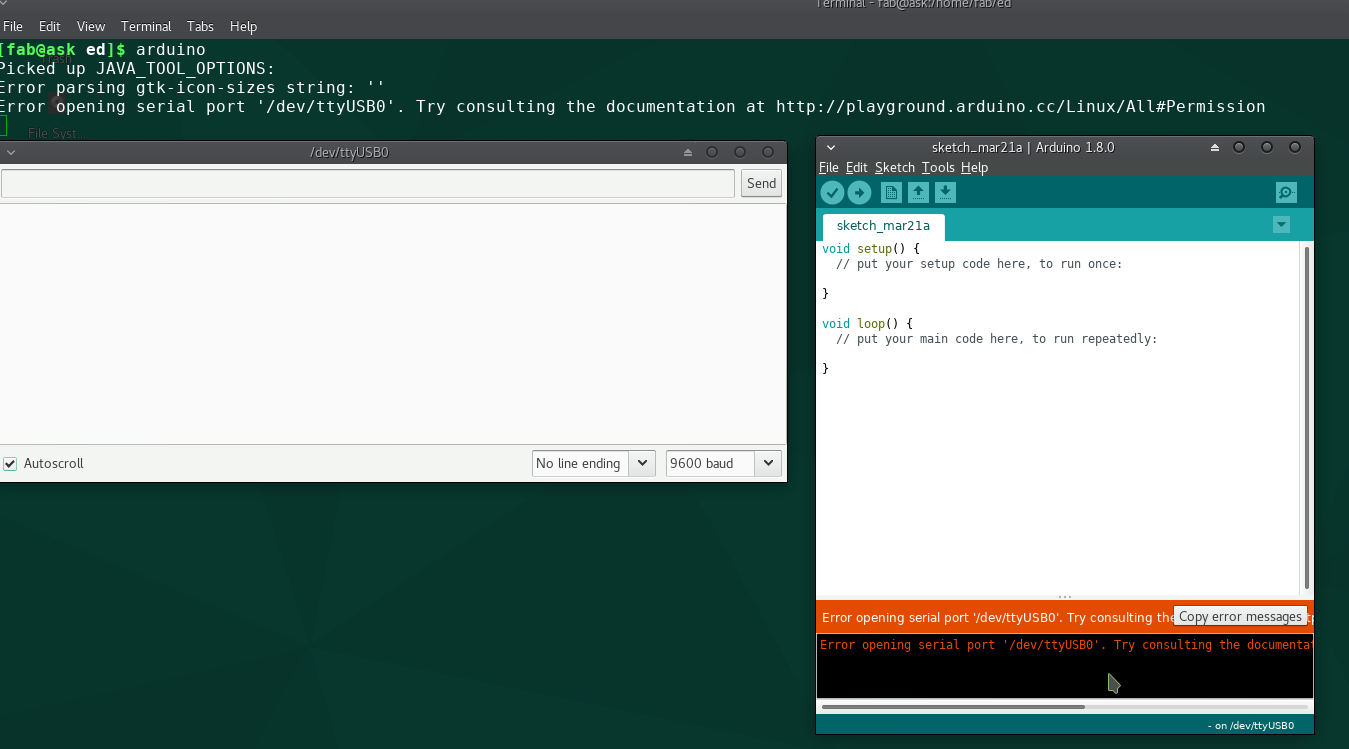
Done again with su permissions
Baud rate is set at 115200 as other values are not giving the expected results.
On checking the code, it is programmed so.
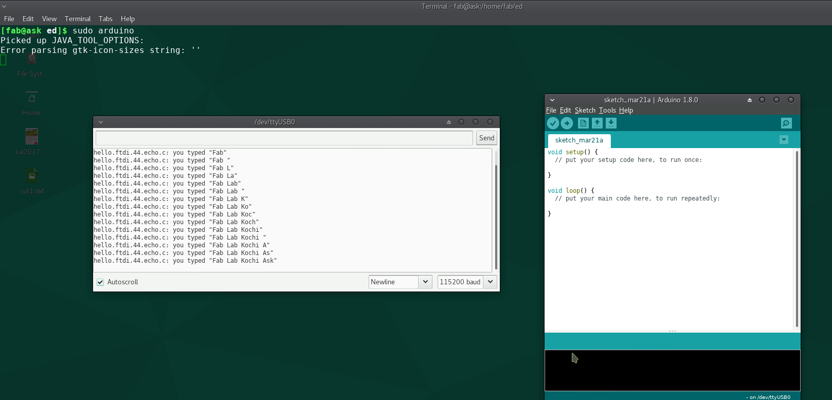
So the circuit board is finally ready!!
The buffer is not cleared. How to do that? We will learn!!
General
(1) We need to ensure that the SVG format is properly handled by the fab module
(2) fab module web version have some apprehensions among fab community - to be addressed
My work
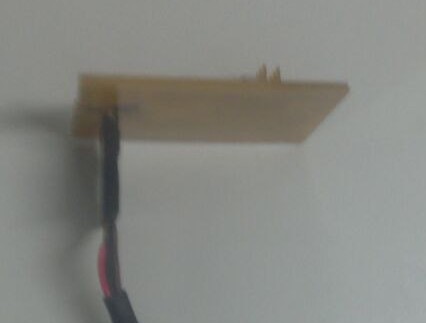
(1) I should have connected the 6 pin connector to the front side of the board instead on the rear side.