week4

Week-6 :-Electronics design (Mar 1)

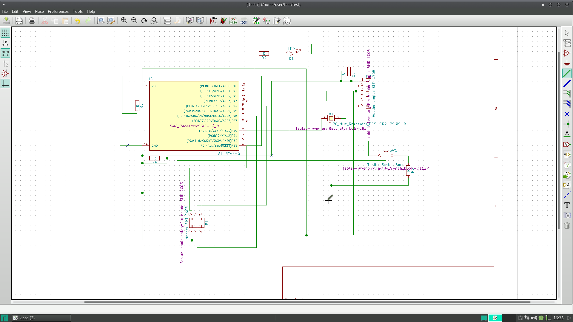
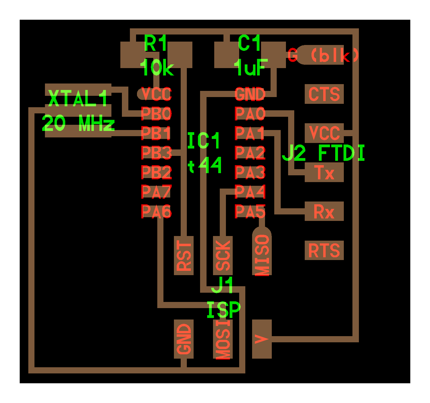
This week assigment is to make a hello-world board. The hello world default board is shown here. The default hello world board contains a microcontroller, an oscillator, a capacitor and a pull-up resistor. The default clock value of microcontroller (Attiny44) is 8 Mhz. We have added an external resonator 20 Mhz to speed up the controller. It's a best practice to add a resonator for precise clock applications.

Pull-up resistors:-
Pull-up resistors are resistors which are used to ensure that a wire is pulled to a high logical level in the absence of an input signal. Pull-up resistors are not a special kind of resistors; they are simple fixed-value resistors connected between the voltage supply (usually +5V) and the appropriate pin, which results in defining the input or output voltage in the absence of a driving signal.
Pull-down resistors:-
Pull-down resistors work in the same manner as pull-up resistors, except that they pull the pin to a logical low value. They are connected between ground and the appropriate pin on a device.
Resistor value

The appropriate value for the pull-up resistor is limited by two factors. The first factor is power dissipation. If the resistance value is too low, a high current will flow through the pull-up resistor, heating the device and using up an unnecessary amount of power when the switch is closed. This condition is called a strong pull-up and is avoided when low power consumption is a requirement. The second factor is the pin voltage when the switch is open. If the pull-up resistance value is too high, combined with a large leakage current of the input pin, the input voltage can become insufficient when the switch is open. This condition is called having a weak pull-up. The actual value of the pull-up’s resistance depends on the impedance of the input pin, which is closely related to the pin’s leakage current. However the resistance value for Attiny 44 is specified in its data sheet as 10KOhm to 20kOhm, We have opted 10kohm resistor for the pull-up.

PCB Design software installation
There are various PCB design softwares available. However I have used Kicad software for the design purpose. Kicad software can run on linux and its free. For the Fablab usage a few additional library need to be added. The additional library can be downloaded here. This library need to be copied on the following location.
step 1:- Usr/share/kicad/library
Also the footprint file need to be copied on the folowing location and can be downloaded here.
step 2:- /usr/share/kicad/footprints/
  • After coping the above two files, open kicad (a new project), click >electronic schematic editor icon.
  • Click Preferences>component librarys> , then add the copied fab library files (above step 1), click ok.
  • Drawing schematic in kicad

    Draw the schematic diagram from the hello world board. Use the following tools 'Place component' , 'place wire' etc. It would be a slightly difficult for the first time, you can use shotcut keys like 'm' for move 'r' for rotate components etc. You could use 0 ohm resistor to complete the PCB at a later stage. I have faced similar problem while designing PCB, and added 0 Ohm resistors in the corresponding schamatic circuits at two locations. In addition to the default hellow-world schematic, we need to add a LED and a switch to the circuit. We can use any free pins on the IC. Since voltage is 5v, the LED need to be protected by a resistor (560Ohm to 1kOhm) will be sufficient depend upon the LED. The switch can be connected to ground through a resistor, say 10kohm. My schematic is shown below.


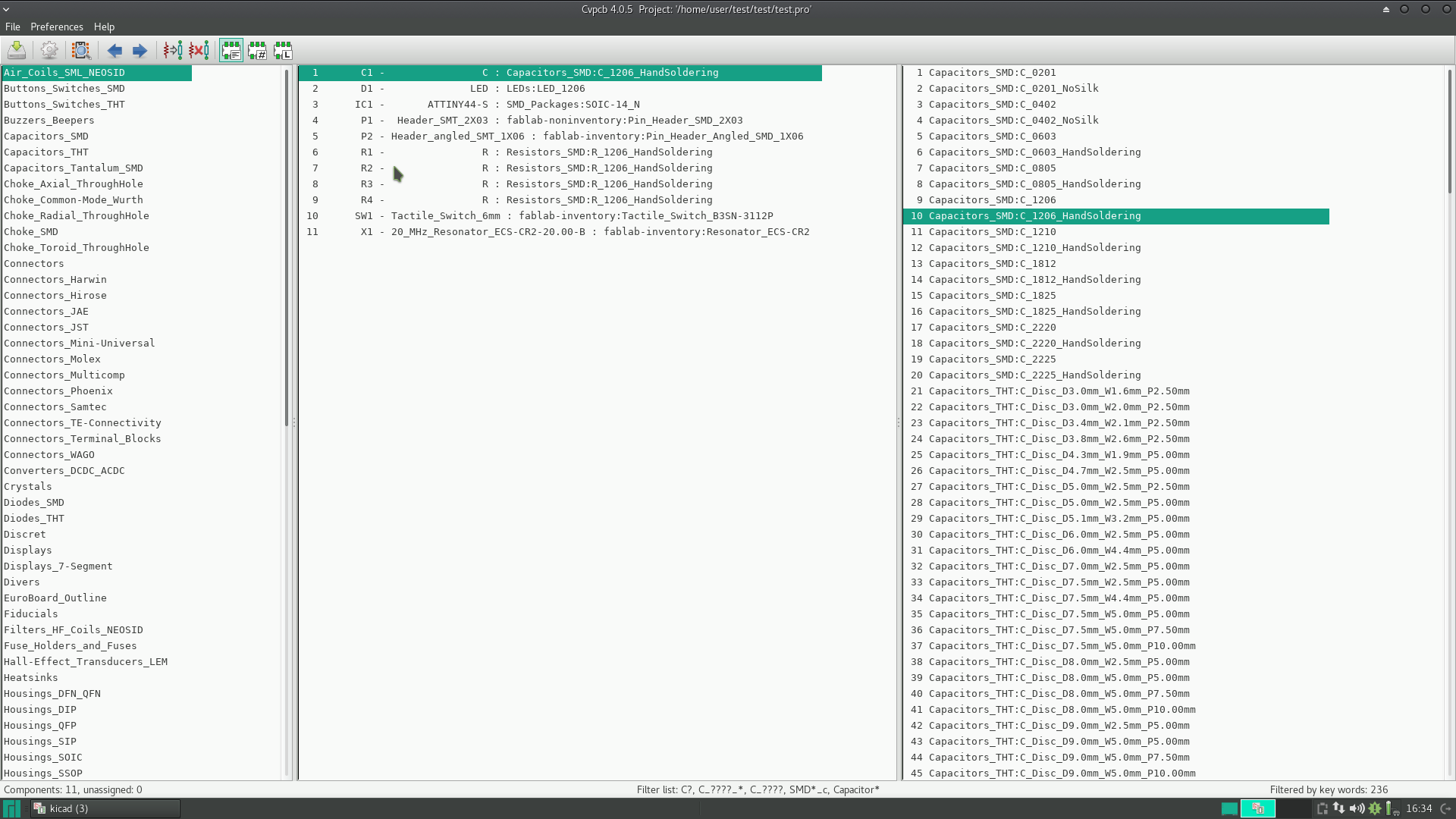
    Once after finishing the schematics click 'generate net list' icon and save. Now we need to assign components to the schematic. Run CvPCB icon, and add the SMD components. Generally 1206 code is used for SMD components like resistors and capacitors. After selecting all components click 'generate net list' and save. Every time you need to repeat this, if you alter your schematic.


    Electrical rule check (ERC):- You can perform an electrical rule check by clicking the ERC icon. This program will check for missing connections, junctions, power supply errors etc. The error location can be easily tracked by clicking the error. You can rectify the main errors.
    Designing PCB in kicad

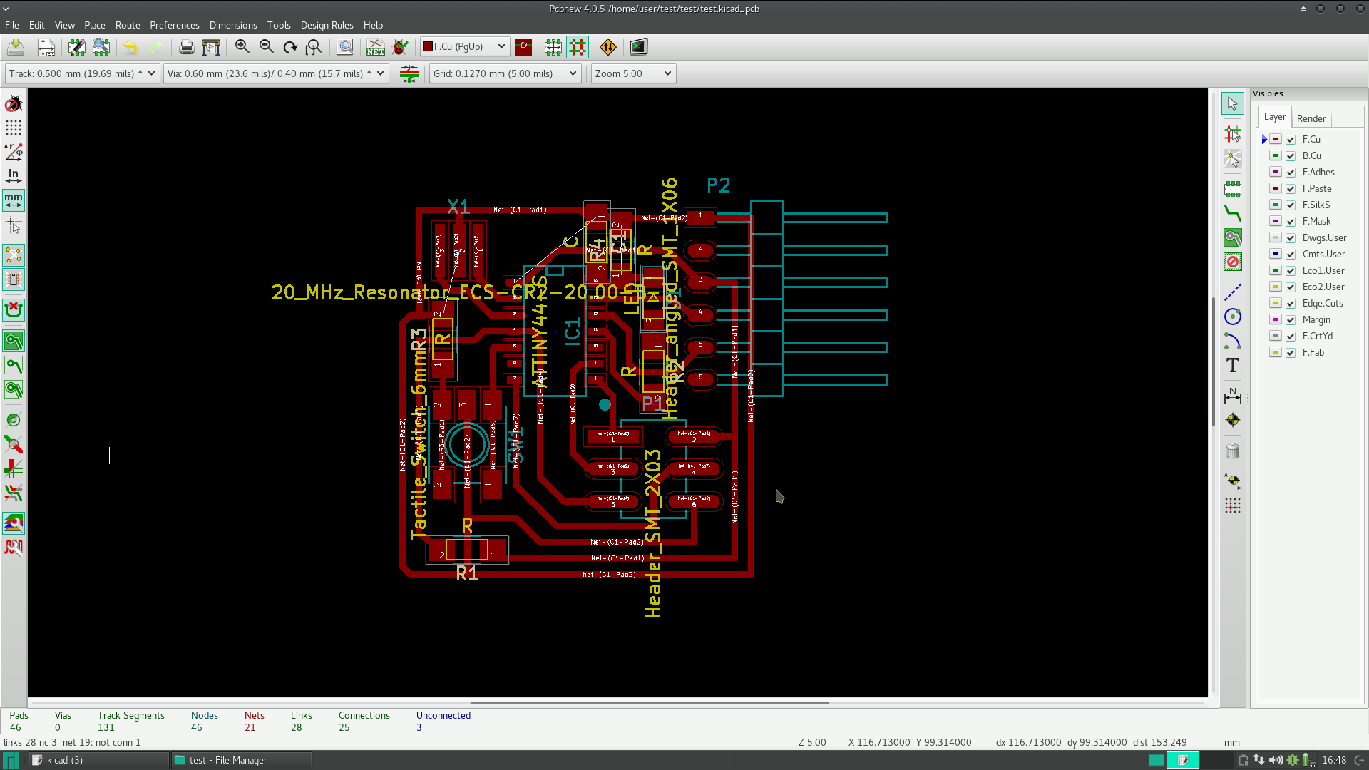
    We are going to design the PCB for a single sided copper clad board. Run Pcbnew icon, this will launch another window. Click the active layer icon and select single track. If You want, you can change the grid to 25mils for better tracks. Click Designrules>design rules>, I have opted 0.5 mm track width, click ok.

  • Click preferences>foot print library manager, add the pretty files in the library tables.
  • Click read netlist icon, click read current net list, now your components are loaded.
  • Now you can place each componets to corresponding locations, and draw the tracks.
  • If required you can turn on autorouting optin by clicking modetrack:autorouting icon, then right click and select autorouting. (I dont recommend autorouting all the time because human brain is much more powerful than that, I learned a simple example, from the issues faced while designing the double track during my project work itself).

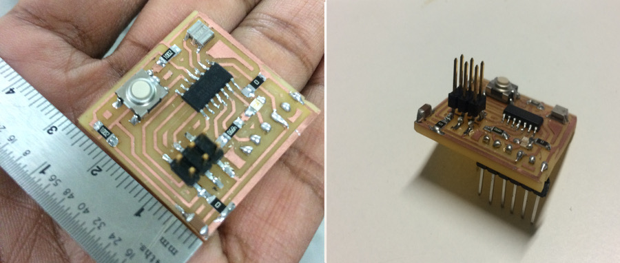
  • There are two 0 Ohm resistors connected to ground terminal at later design, However those two wires need not be routed, since it's connected to ground already. My PCB drawing is shown below. All the components are placed in such a way to reduce the size of PCB within 3cmx3cm. However, I wish I could make it even smaller. All the schematics and PCB design files are available for download here.


    Design rule check (DRC):- After designing the tracks, you can do a design rule check by clicking the DRC icon. The values I opted for the design is given below.
  • Track Clearance:- 0.4 mm
  • Track width:- 0.5 mm
  • Via Dia:- 0.6 mm
  • Via drill:- 0.4 mm
  • Global design rules
  • Minimum track width:- 0.2 mm
  • Minimum via dia:- 0.4 mm
  • If your design is perfect, you wont get any errors. I got a few errors while running DRC, that is because of the 0 Ohm resistors I added on latter stage are assigend to ground and share same terminal through 0 Ohm resistors, so I decided to go ahead with my PCB design.
    PCB milling
    For milling operation in modella machine, you could save/print the file the PCB as SVG, and do the milling. If you need png file, kicad doesnt have a direct step to export into png format, instead you can follow the below two steps to get very high resolution png format file.
  • step 1:- Click file > print (select the required layer, click black and white) > then click print.
  • step 2:- Select the file to print, click SVG format and save.
  • step 3:- Open your svg format in inkscape and save as png. (By default the image is croped automatically, select the required resolution and dpi). The corresponding SVG and PNG format file can be downloaded here.


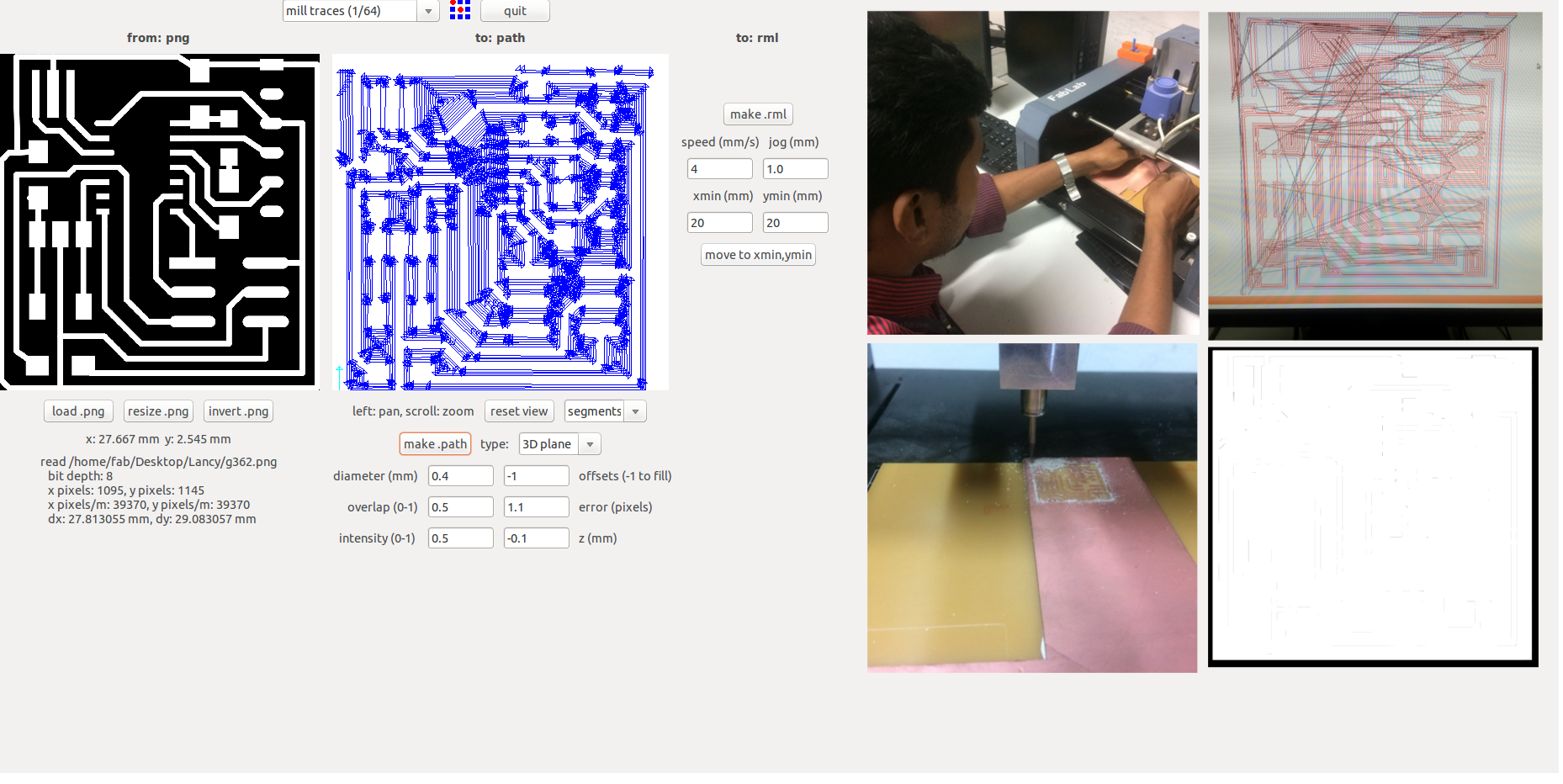
    The PCB milling is done using Modella MDX 20 machine. Open the terminal window using fab command, and open the svg/png file. Parameters for milling operation is shown in the below picture. You can do complete milling by setting offset parameter = -1. The milling operation is done using 1/64" drill bit and PCB cutting by 1/32" tool bit.


    List of components.
  • Microcontroller:- Attiny 44
  • 2/4 pin tactile switch
  • Resistors :- 10K-2nos, 0 Ohm -2nos, 490 Ohm
  • 20Mhz crystal oscillator
  • SIL horizontal male header pins
  • 2x3 header pin
  • The SIL horizontal male pins are costly and not easily available. This can be replaced by straight male header pins. You need to dill the holes accordingly for the 6 pins. All the components were soldered along with the male header pins. For better soldering, you can add soldering flux.


    Checking communication
    The Attiny44 microcontroller communication can be checked using FabISP. The following command is used to check the communication.
    sudo avrdude -c usbtiny -b 9600 -p t44
  • Avrdude is the driver program for Atmel microcontroller.
  • -c option is for specifing the programmer followed by its name, here its FabISP. ie, usbtiny. This device can be checked by entering the command "lsusb" in terminal window.
  • -b option is the baudrate followed by the speed.
  • -p option identify the device to which the programmer is attached.
  • t44 is for Attiny44, You can check the list of supported device by entering the command "avrdude -c avrisp" in terminal window.
  • The output from the above command is shown below.

  • It depicts that the device is initialized.
  • The device name t44 is shown in bracket along with its signature (each microcontroller have its own signature).
  • It also depicts the factory default fuse informations E:FF, H:DF, L:62.


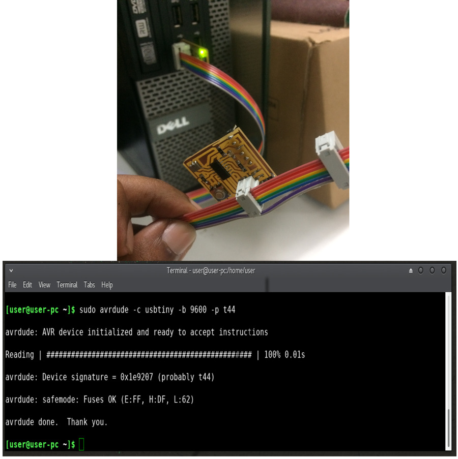
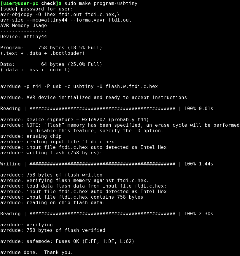
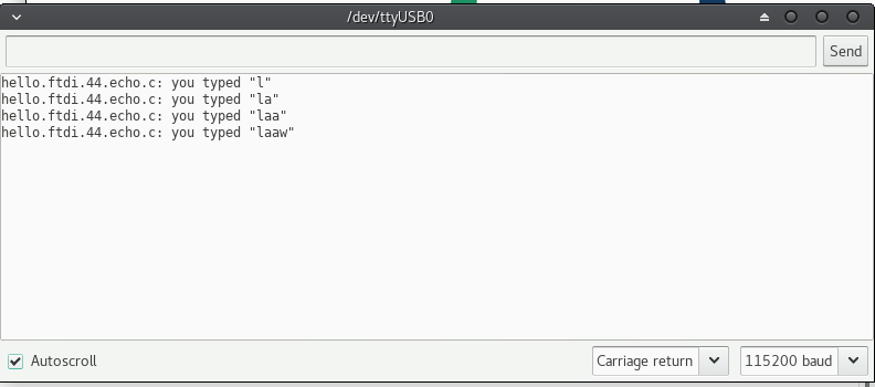
  • Finally the Attiny44 need to be programmed and connected to FTDI cable. The program tells to read character typed through keyboard and and display in the table. Installed the Arduino software and opened tools>port>devttyUSB0.Then click tools>serial monitor, they type the characters. The files for compiling can be downloaded from here. The folowing comands are used for compiling the files.

    sudo make program-usbtiny
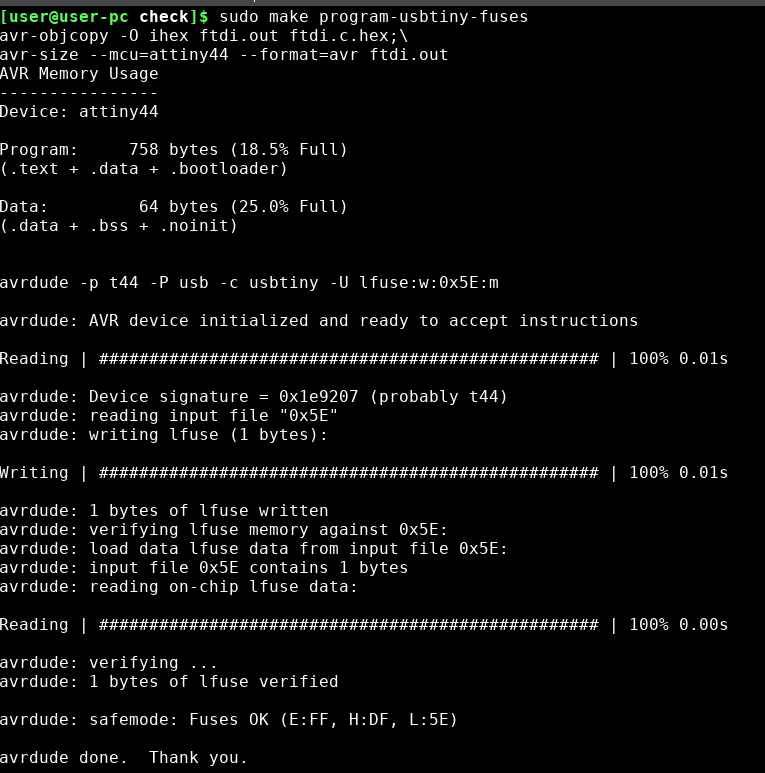
    sudo make program-usbtiny-fuses