
- Add an output device to a microcontroller board you've designed and program it to do something
Class material: Output Devices
Insper FabLab's operational manual here.
Roland MDX-40A - Machine's tutorial, please click here.
One may also check this tutorial explaining how to mill a coin (and how to operate and setup the working material in a machine like Roland MDX-40A). The manufacture link to its own documentation and information will be found here.
CNC is a technology that allows one to produce code and with it 'tells' a machine what to do in any given point inside its working area. The CAD tool works with desing, or the initial creative step of any project. After that, when there is the need to manufacture it - and therefore CNC technology is demmanded - another kind of software is needed: CAM is the software that creates the machine program from a digital design. During FabAcademy, most of my projects will be developed in Fusion360 CAD tool or Eagle 8.0 schematic/board tool and, from there, Fabmodules will be the next step as CAM tool.
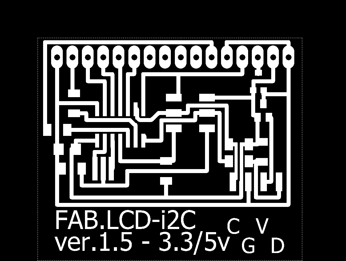
This week assignment is a PCB that has an LCD that works as output device. I will work based on Kenzo's project. His project is made for a display with 16 columns and 4 rows. I will adapt it to a display with 16 columns and 2 rows.
It follows the standard setup for the machine and tools we have here at Insper for FabModules and Roland MDX-40A.
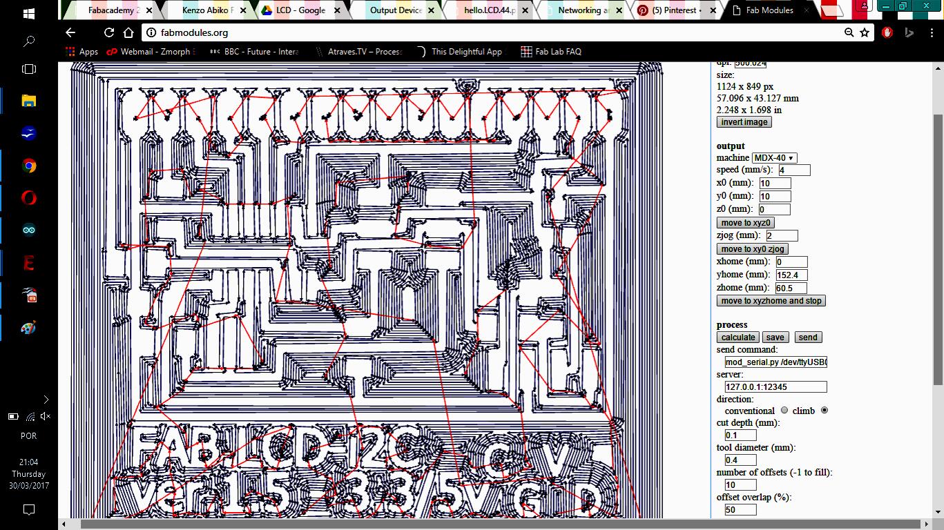
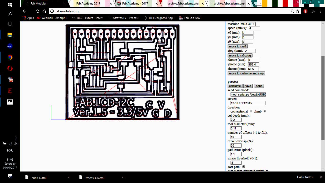
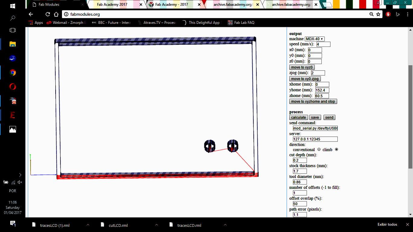
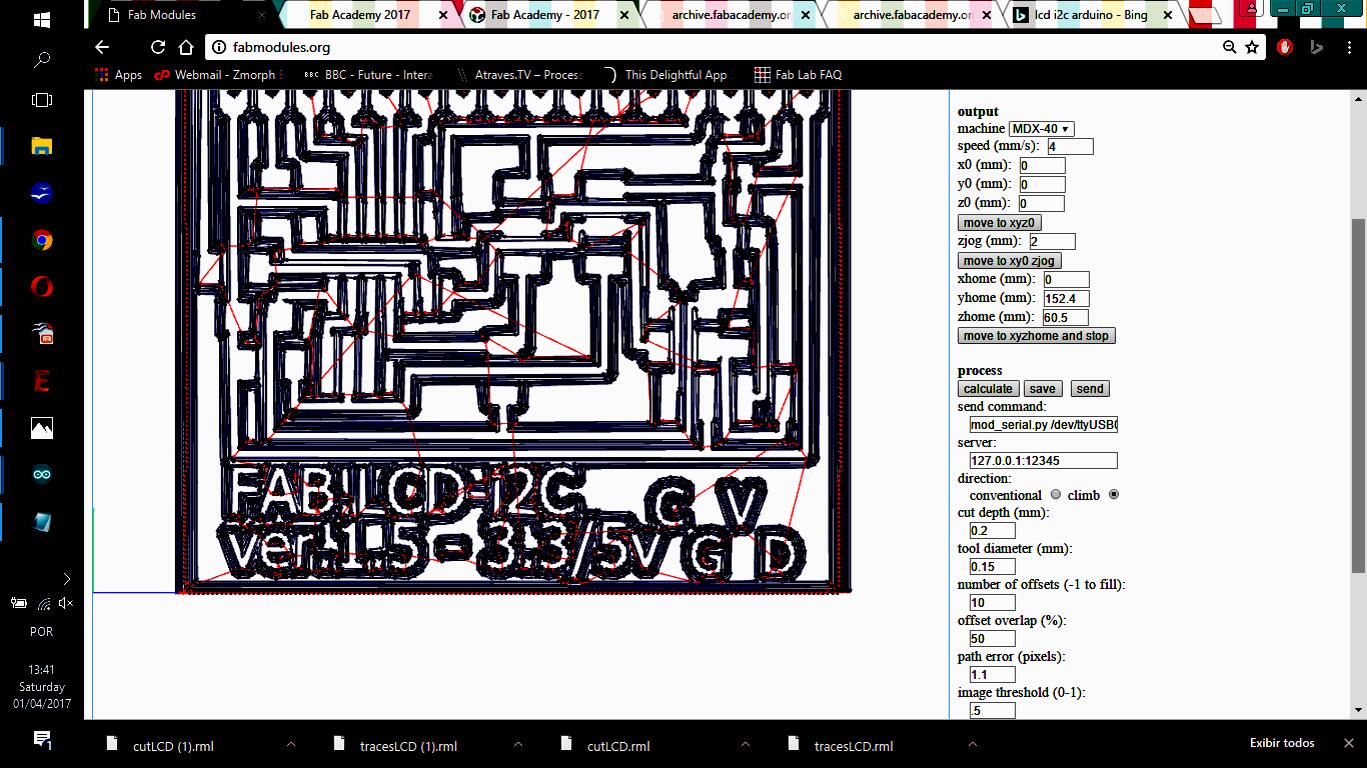
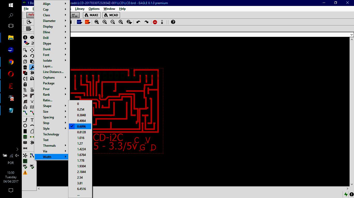
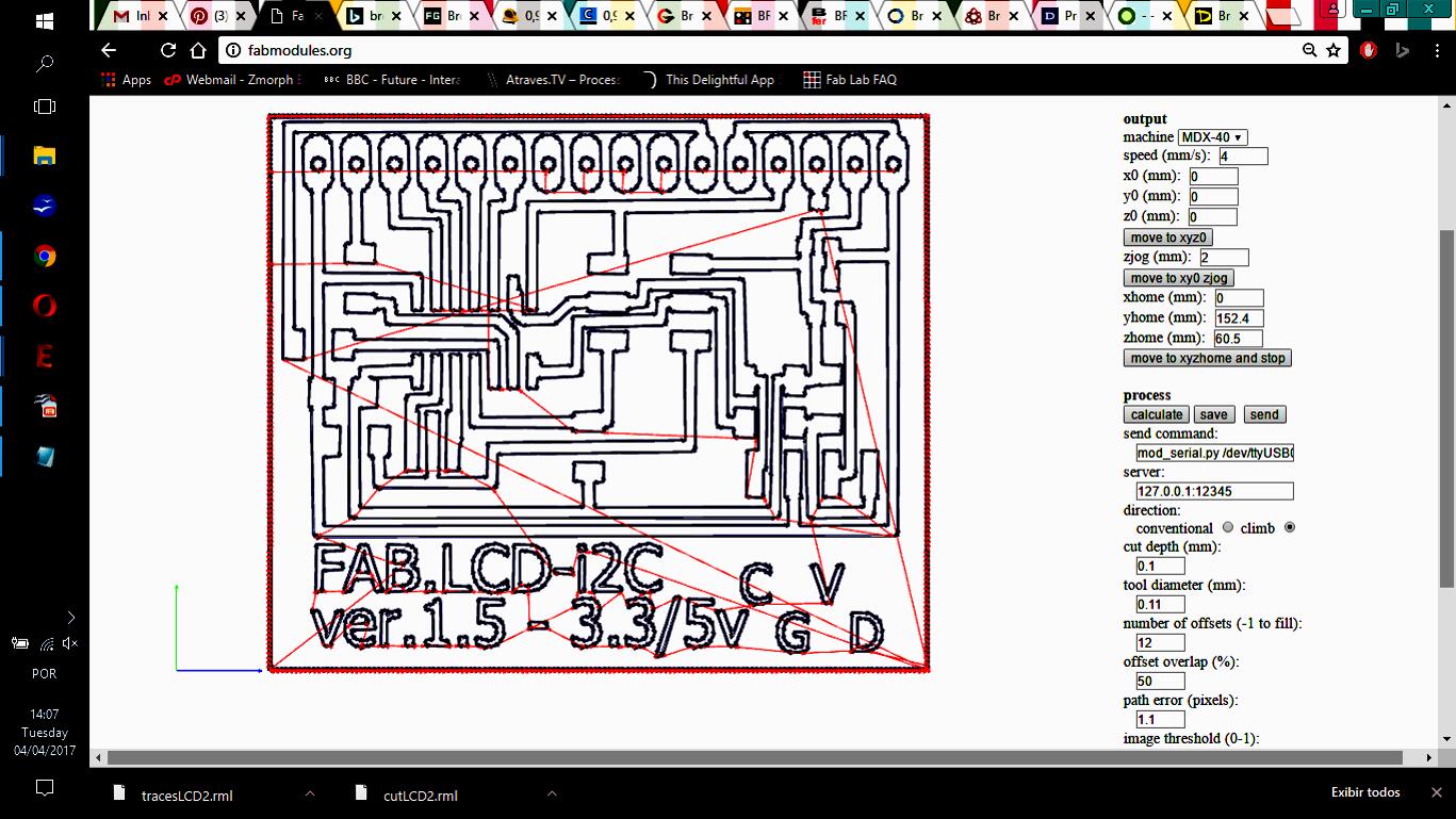
Input: this is an image file png that will describe the traces or cut need on the board. Select the image you need for each PCB. This exercise has this final board design for traces and this final board design for outline. The traces thickness was the most important change in all boards (select a wider trace makes easier to sold and the board more resistent) - target value: 0.80 mm.
My Global evaluator made some comments about the PNG files that are improtant to share.
Pradnya's comment
"
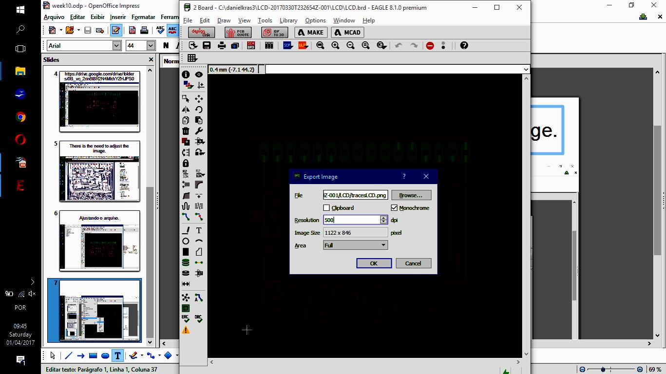
In case of milling out the exterior you can not directly use the png files generated from eagle software. That is the reason your outside traces have also been milled. There are different way you can handle this. One way is to generate the trace file with sufficient margin and use 2d raster editing software such as gimp or photoshop to draw a thick outline. The ther reason for failure is that you not inverted the image. By default white parts of an image are preserved by fab modules and the tool offset if provided on the black side of the png image. In case of cutout line the border should be black and interior should be white. It this opposite the toolpath generated will lead to interior of the border being cut rather than the exterior which is required.
"
I made a second version for the cut file. For that one, please, click here.
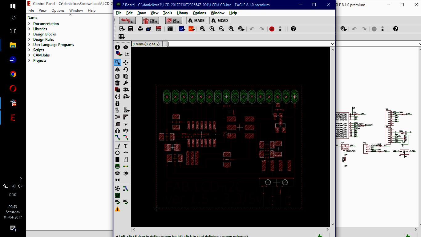
Desing files:
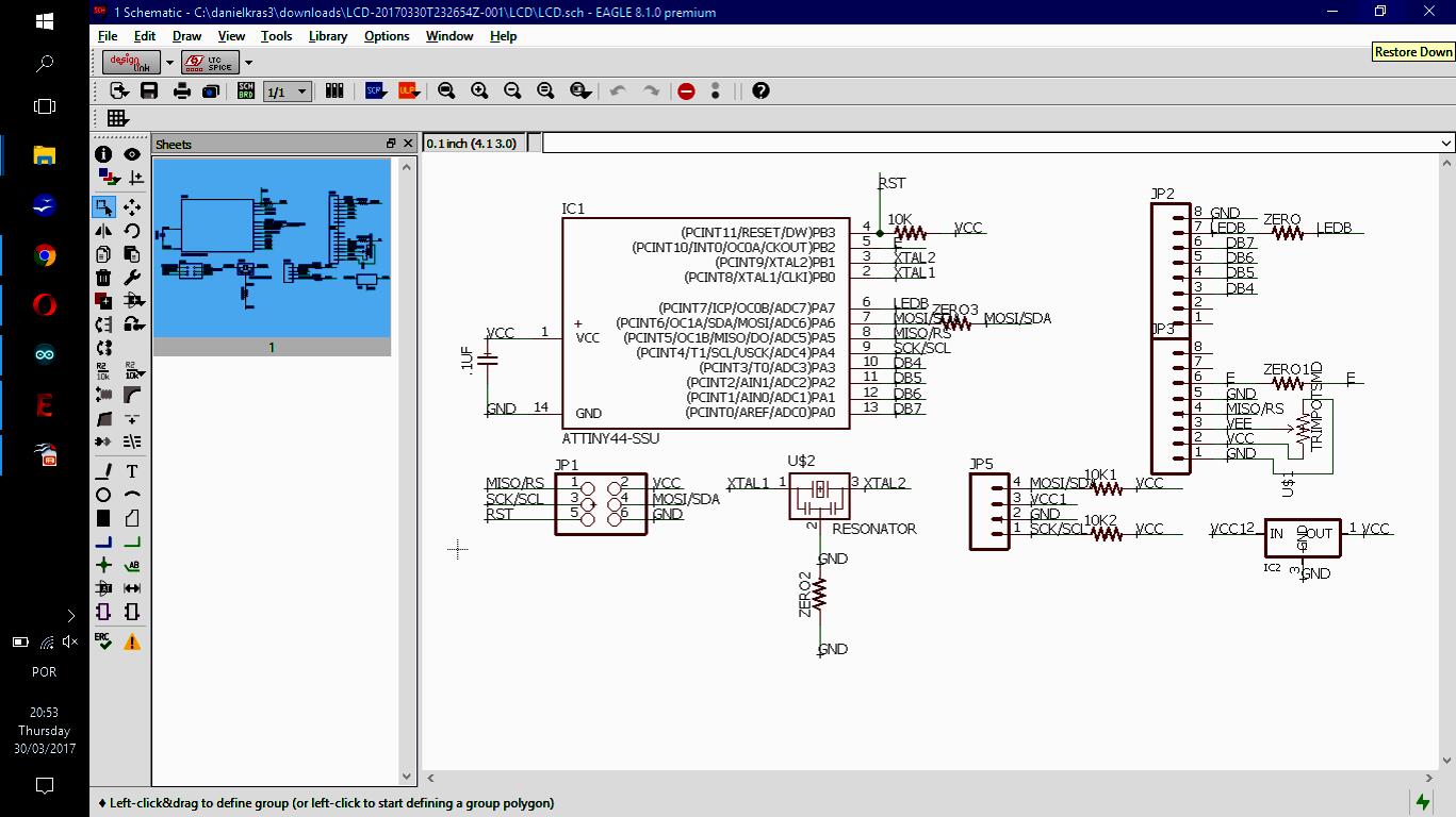
- Schematic: LCD sch.
- Board: LCD brd.
- Relay final edition - schematic.
- Relay final edition - board.
- Relay PNG image - traces.
- Relay PNG image - cut.
- SparkFun Ealge libraries.
- Adafruit Eagle libraries.
Output format: Roland Mill (.rml) - this selection will set the FabMoludes to work with a milling machine.
Process: if the selected option is 'PCB traces' than
--- Machine = Roland MDX-40A
--- x0 (mm) = 0
--- y0 (mm) = 0
--- cut depth (mm) = 0.2
--- tool diameter (mm) = 0.11
--- number of offsets = 8
--- offset overlap (%): 50
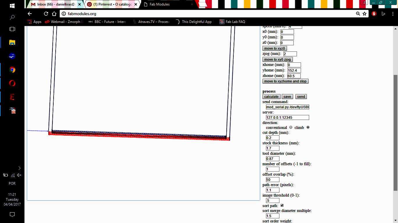
Process: if the selected option is 'PCB outline' than
--- Machine = Roland MDX-40A
--- x0 (mm) = 0
--- y0 (mm) = 0
--- cut depth (mm) = 0.2
--- stock thickness (mm) = 1.7
--- tool diameter (mm) = 2.00
--- number of offsets = 1
You may adjust the setup once you have different milling tools. As the phenolite paper changes from batch to batch, there is the need to compensate ondulations and assimetry eventualy.
PRESS: "Calculate" button to check how the simulation goes on your computer. Observe if the mill process remove material where it is supposed to and leave material untouched the same way.
PRESS: "save" button in order to have the rml file in your computer.
FabModules allows its user to make other specifications and different setups. I only made reference to the ones needed for PCB milling. Anyother setup may be left the way it comes preseted.
LCD board - Traces;
LCD board - Outline.
- Relay traces - rml.
- Relay cut - rml.
Once the rml program is done, there is the need to move from computer setups to machine operation. Roland's Vpanel program is part of machine's manual (click here); some extra information is displayed below.
The machine needs to be power on in order to comunicate with Vpanel software.It follows some images of Vpanel Operation to config a new job.


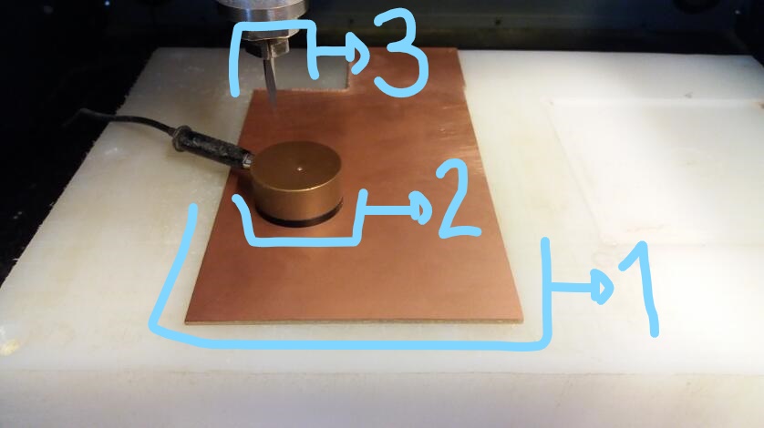
Phenolic paper - copper layer for circuit boards - standard 1,7 mm thickness - example here.
Mill - engraver - 20°edge - example here.
Mill - endmill - 2,00 mm cut diameter - 02 flutes - example here.
This assignment has two objects:
- A LCD board - this was a Kenzo documentation implementation.
- A Relay board - this is part of my final project. It complements the assignment task.
----- The microcontroler board information will be found in Exercise13 webpage.
----- Relay board has the task to controlswitch the heat actuator.
LCD BOM list will be displayed below.
Partlist exported from week10-LCD-KenzoBoard-01.sch
| Part | Value | Device | Package | Description | |
| .1UF | UNPOLARIZED_CAPACITOR1206 | 1206 | unpolarized_capacitor | ||
| 10K | RES-US1206FAB | R1206FAB | Resistor (US Symbol) | ||
| 10K1 | RES-US1206FAB | R1206FAB | Resistor (US Symbol) | ||
| 10K2 | RES-US1206FAB | R1206FAB | Resistor (US Symbol) | ||
| IC1 | ATTINY44-SSU | ATTINY44-SSU | SOIC14 | ||
| IC2 | REGULATORSOT23 | SOT23 | |||
| JP1 | PINHD-2X3-SMD | 2X03SMD | PIN HEADER | ||
| JP2 | M08LONGPADS | 1X08_LONGPADS | Header 8 | ||
| JP3 | M08LONGPADS | 1X08_LONGPADS | Header 8 | ||
| JP5 | M04SMD | 1X04-SMD | Header 4 | ||
| U$1 | TRIMPOTSMD | TRIMPOTSMD | TRIMPOT-3MM | ||
| U$2 | RESONATOR | RESONATOR | EFOBM | ||
| ZERO | RES-US1206FAB | R1206FAB | Resistor (US Symbol) | ||
| ZERO1 | RES-US1206FAB | R1206FAB | Resistor (US Symbol) | ||
| ZERO2 | RES-US1206FAB | R1206FAB | Resistor (US Symbol) | ||
| ZERO3 | RES-US1206FAB | R1206FAB | Resistor (US Symbol) |
| Part | Value | Device | Package | Description | MF | MPN | OC_FARNELL | OC_NEWARK |
| DIODE | 1N4148DO35-7 | 1N4148DO35-7 | DO35-7 | DIODE | ||||
| JP1 | PINHD-1X2 | 1X02 | PIN HEADER | |||||
| K1 | CQ1-12V | CQ1-12V | CQ1 | AUTOMOTIVE QUIET RELAY NAiS | unknown | unknown | ||
| LED1 | LED5MM | LED5MM | LED | |||||
| R1 | 4700 | R-EU_0204/7 | 0204/7 | RESISTOR, European symbol | ||||
| R2 | 330 | R-EU_0204/7 | 0204/7 | RESISTOR, European symbol | ||||
| SV1 | MA03-1 | MA03-1 | PIN HEADER | unknown | unknown | |||
| T1 | BC547 | BC547 | TO92 | NPN TRANSISTOR |
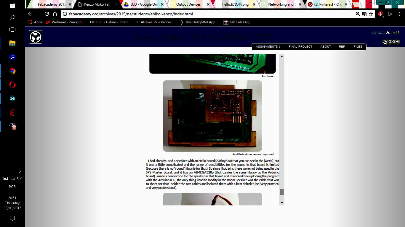
LCD display was the choice for this assignment after discussing the topic with Kenzo. He made himself a LCD display board and conections when a fabber. I will start my project based on his documentation.
The idea of implementing a display is good once I may assemble it to the coffee maker as a way to comunicate its process/status to coffee consumers/users.
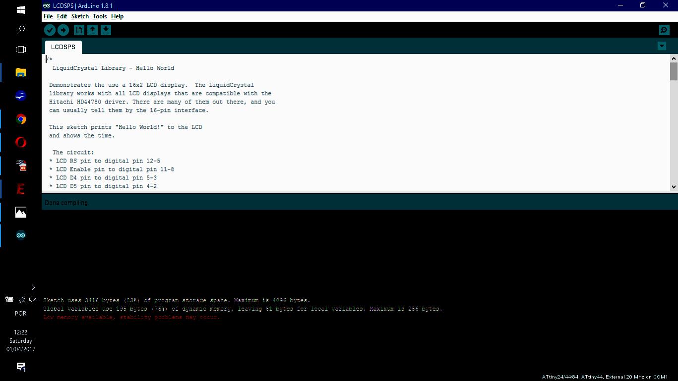
I took me several times to make a good .rml code and mill the board (FabModules as .rml generator and the machine was a Roland MDX-40. After that, I took me a while to fix the board (I needed to implement some extra jumpers). I was missing a component and I changed the potentiometer for a resistor. I missed a second jumper in the board; that was fixed with Kenzo's help.
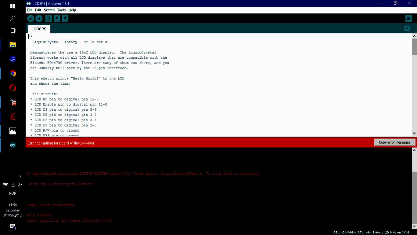
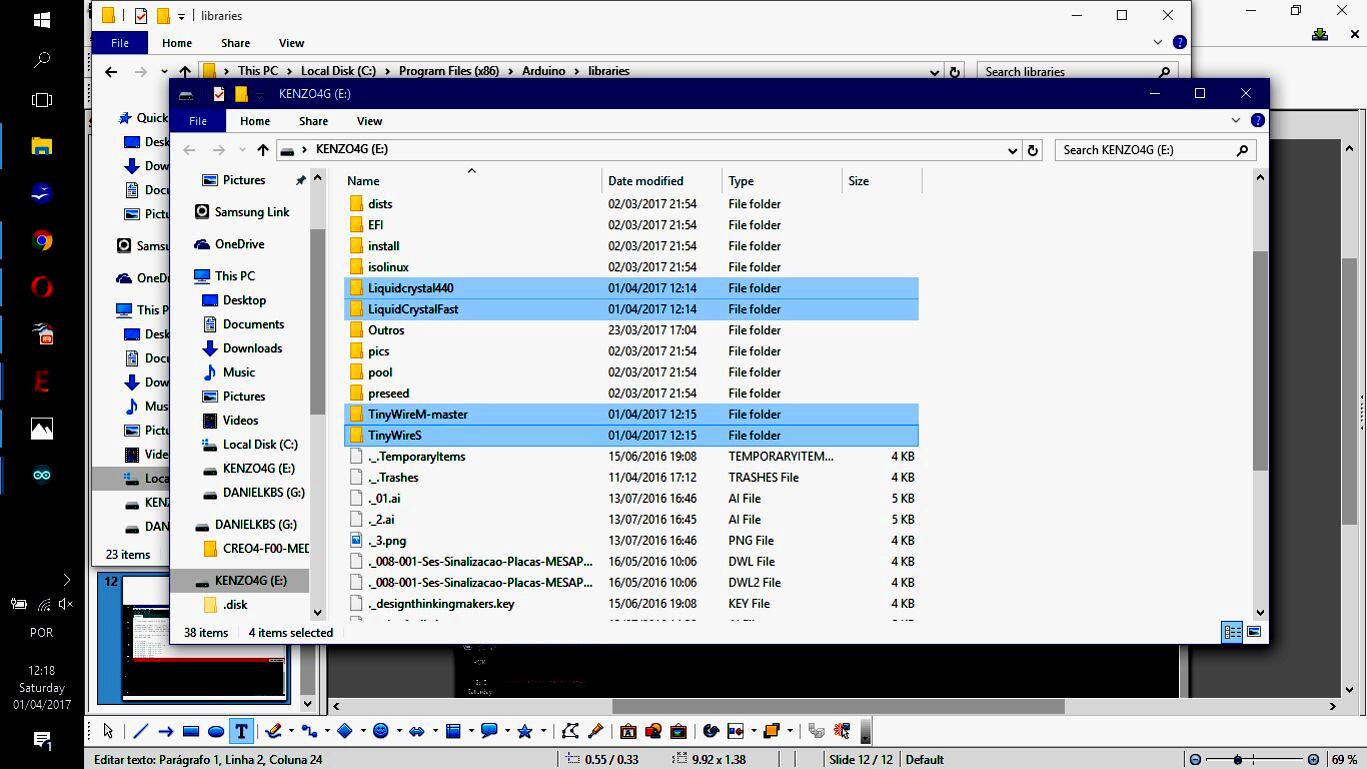
The first code test took me a while too. I had to install some libraries to work with Arduino software. I run Kenzo's code for the LCD and it worked not so well. His display had 04 rows and mine has only 02 rows. The last test is a new code that I wrote.


small.jpg)
small.jpg)
small.jpg)
small.jpg)
small.jpg)
small.jpg)
small.jpg)
-----------

This work is licensed under a Creative Commons Attribution-ShareAlike 4.0 International License.