
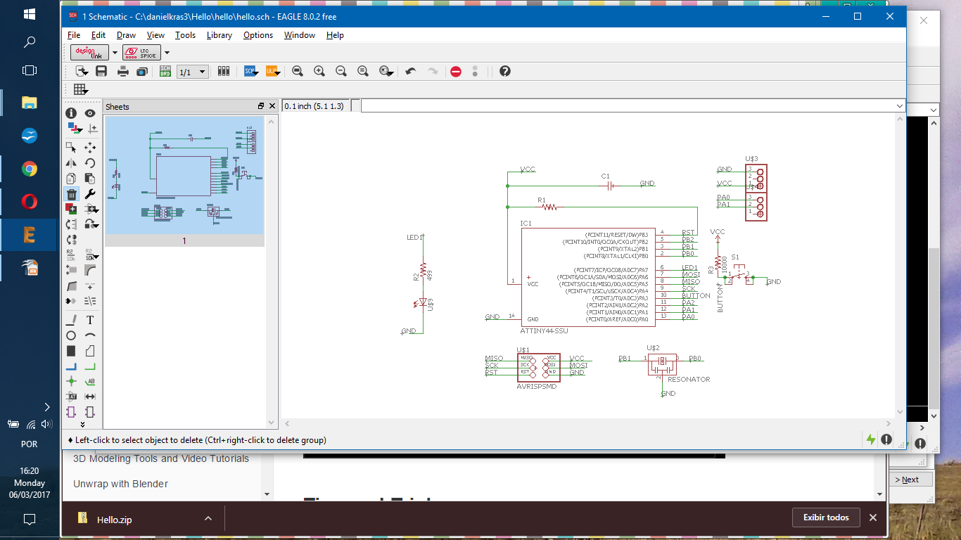
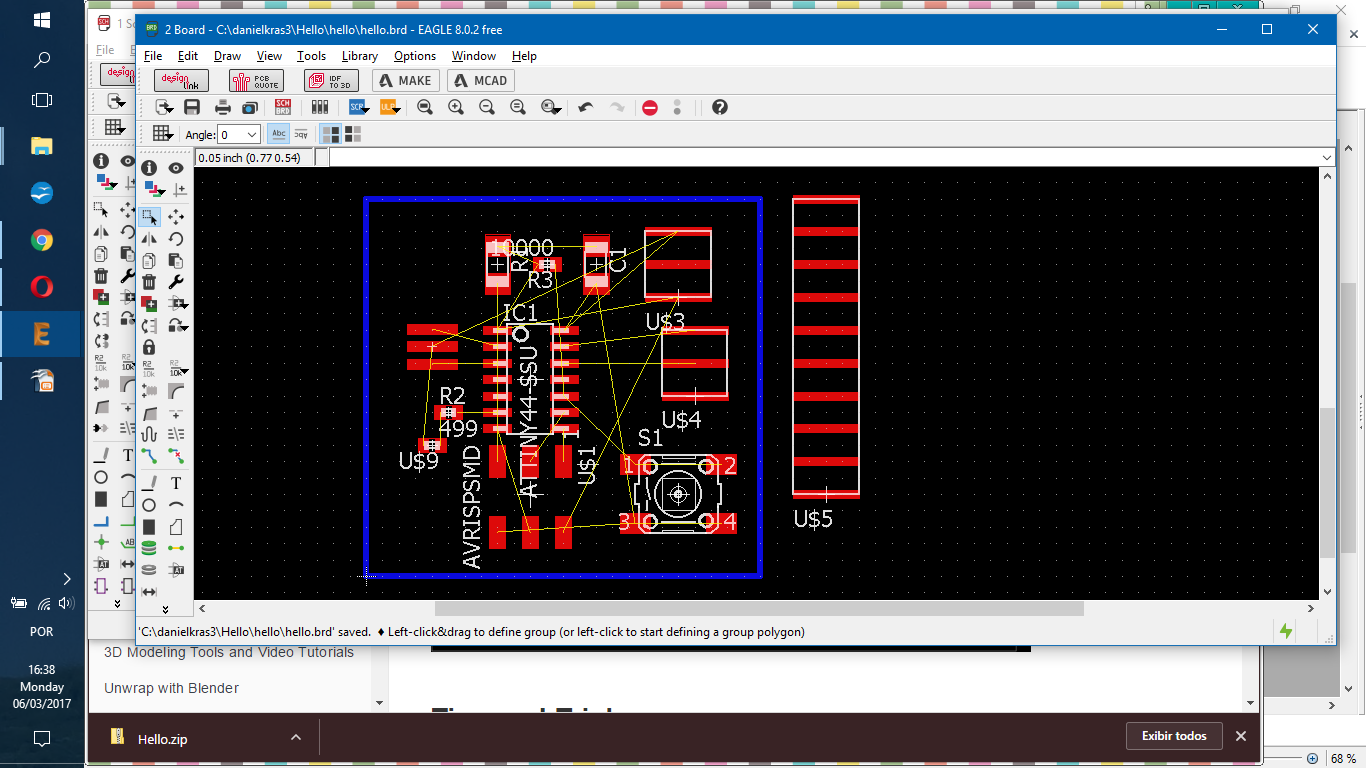
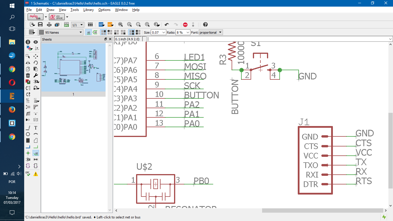
- Redraw the echo hello-world board, add (at least) a button and LED (with current-limiting resistor), check the design rules, make it (if you have time this week, test it).
Class material: Electronics Design
Insper FabLab's operational manual here.
Roland MDX-40A - Machine's tutorial, please click here.
One may also check this tutorial explaining how to mill a coin (and how to operate and setup the working material in a machine like Roland MDX-40A). The manufacture link to its own documentation and information will be found here.
-----------------------------------
Desing files:
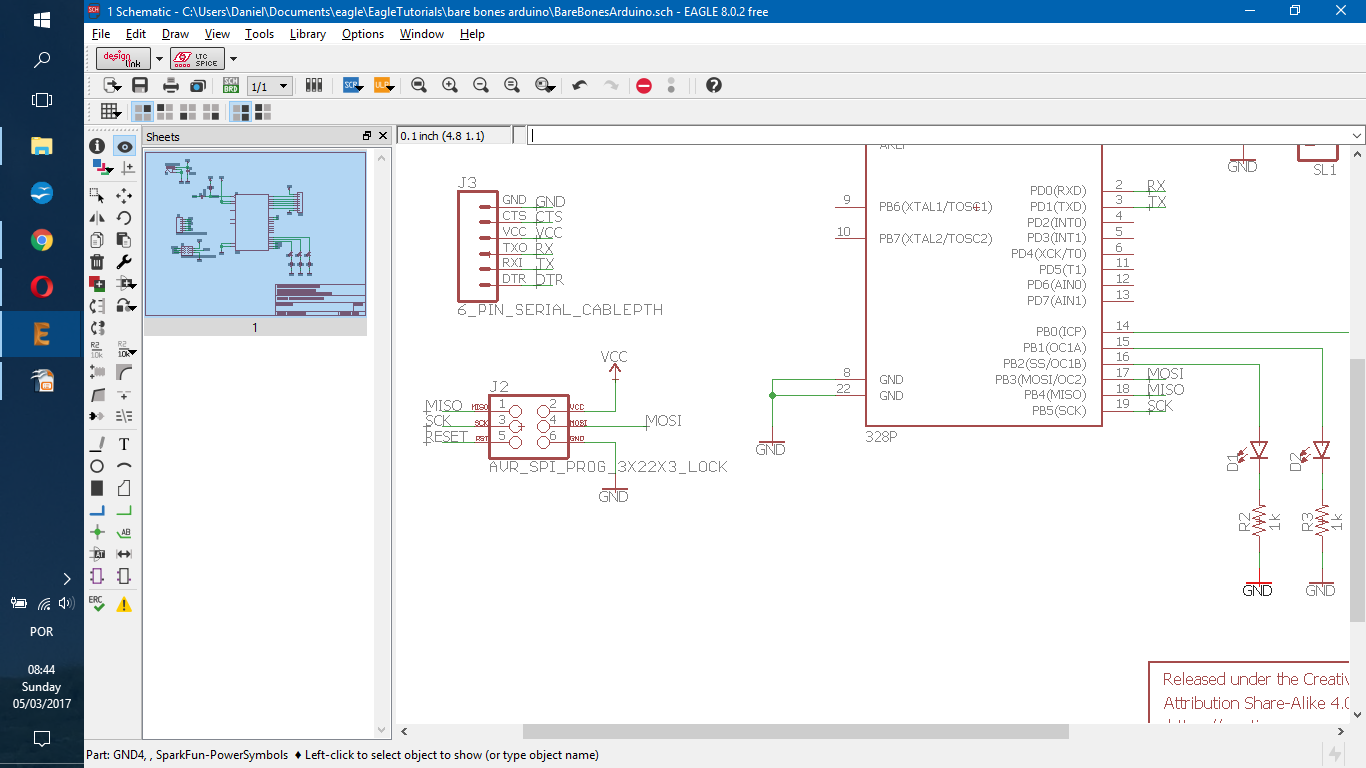
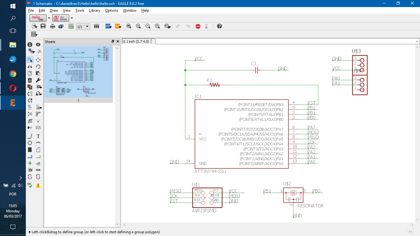
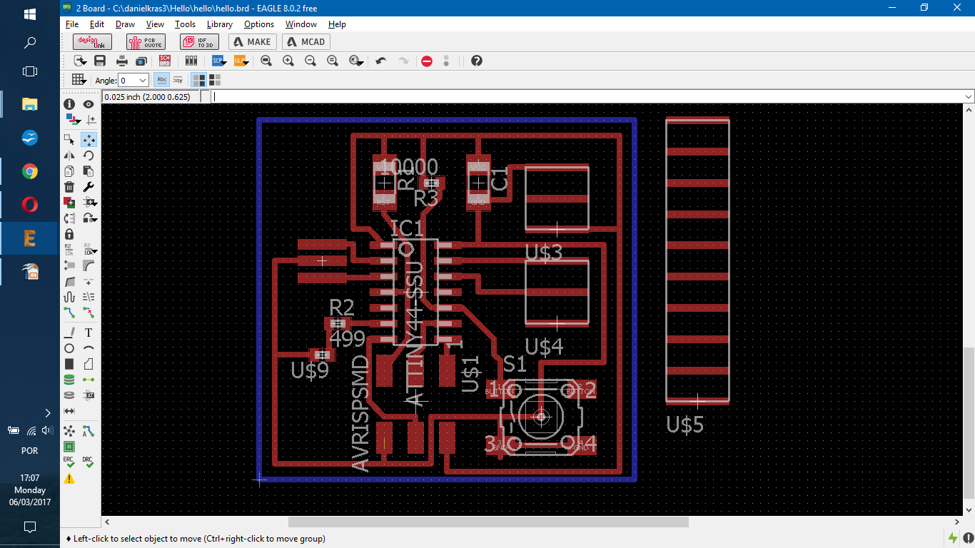
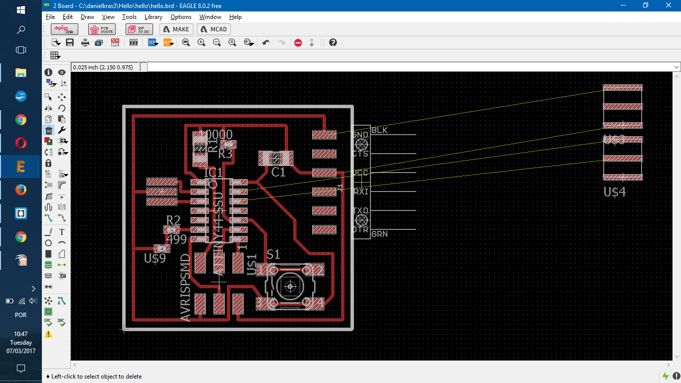
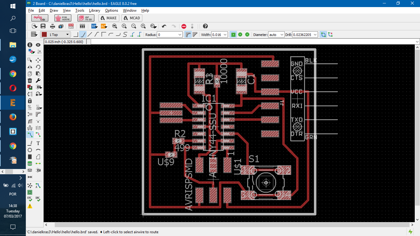
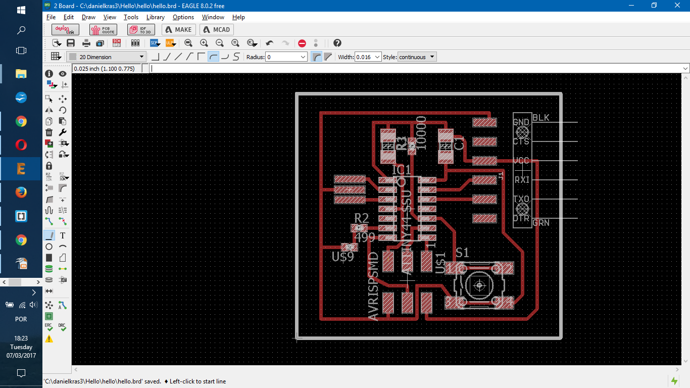
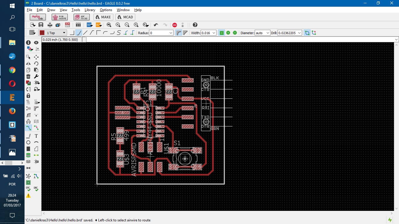
- Schematic: new hello sch.
- Board: new hello brd.
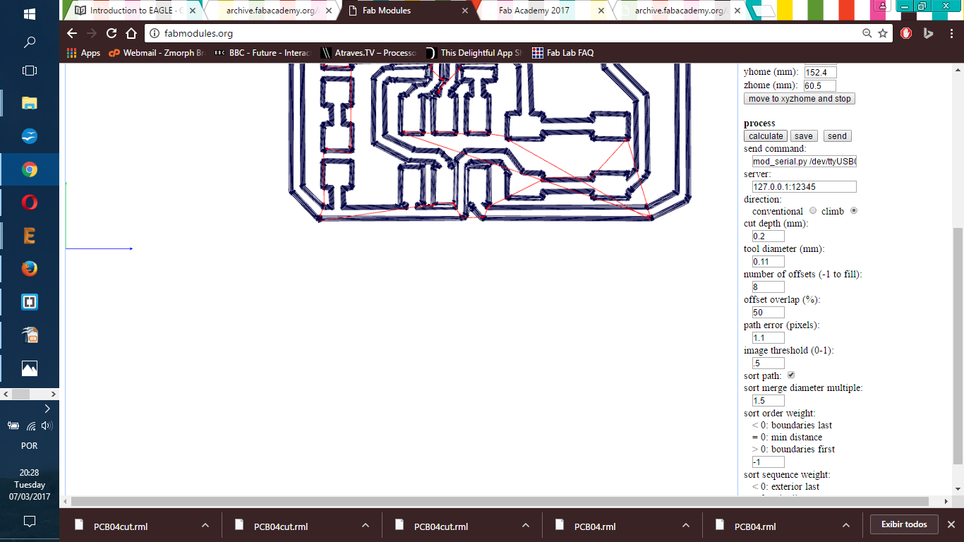
CNC is a technology that allows one to produce code and with it 'tells' a machine what to do in any given point inside its working area. The CAD tool works with desing, or the initial creative step of any project. After that, when there is the need to manufacture it - and therefore CNC technology is demmanded - another kind of software is needed: CAM is the software that creates the machine program from a digital design. During FabAcademy, most of my projects will be developed in Fusion360 CAD tool or Eagle 8.0 schematic/board tool and, from there, Fabmodules will be the next step as CAM tool.
This week assignment is a PCB that has an inicial design and it is supposed to be edited. Further notes will explain better about Eagle 8.0 which is the design tool I used for PCB design.
It follows the standard setup for the machine and tools we have here at Insper for FabModules and Roland MDX-40A.
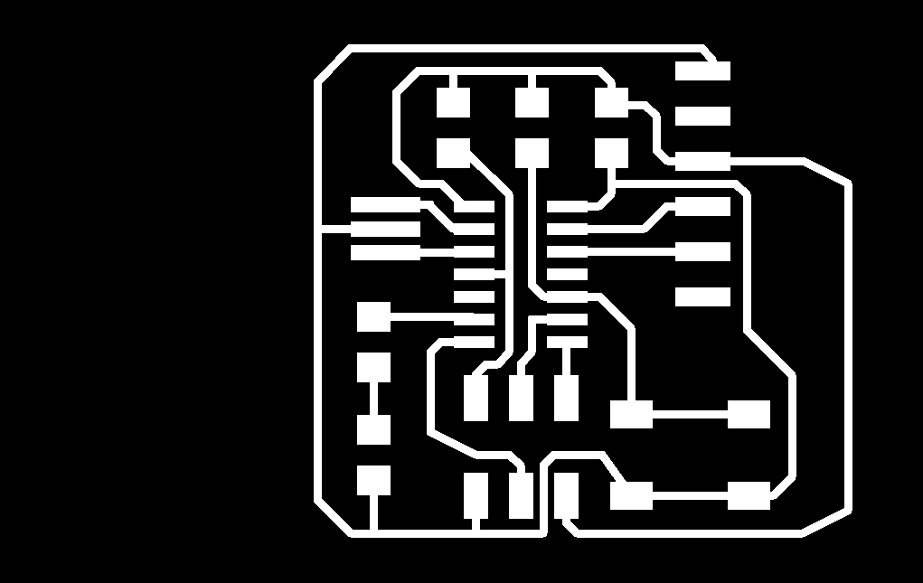
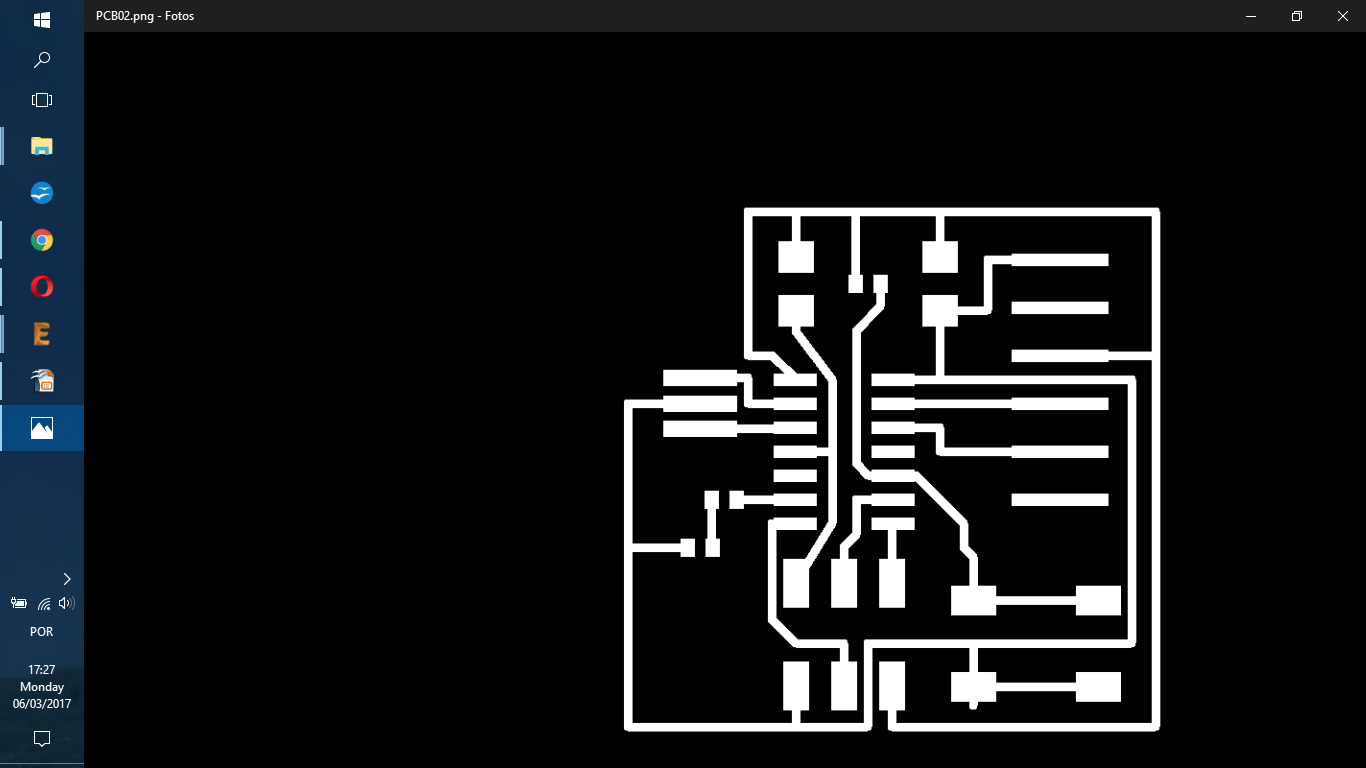
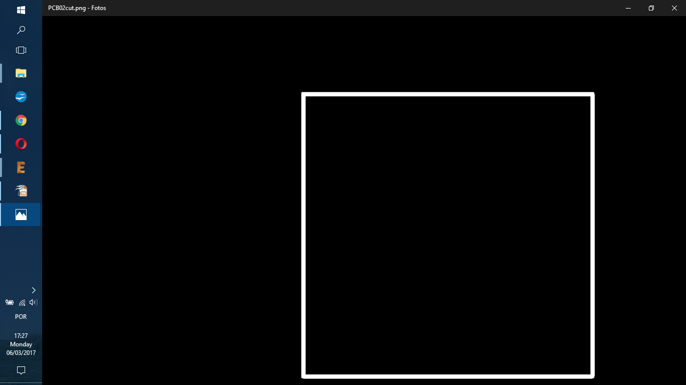
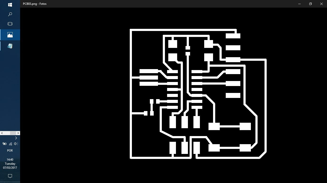
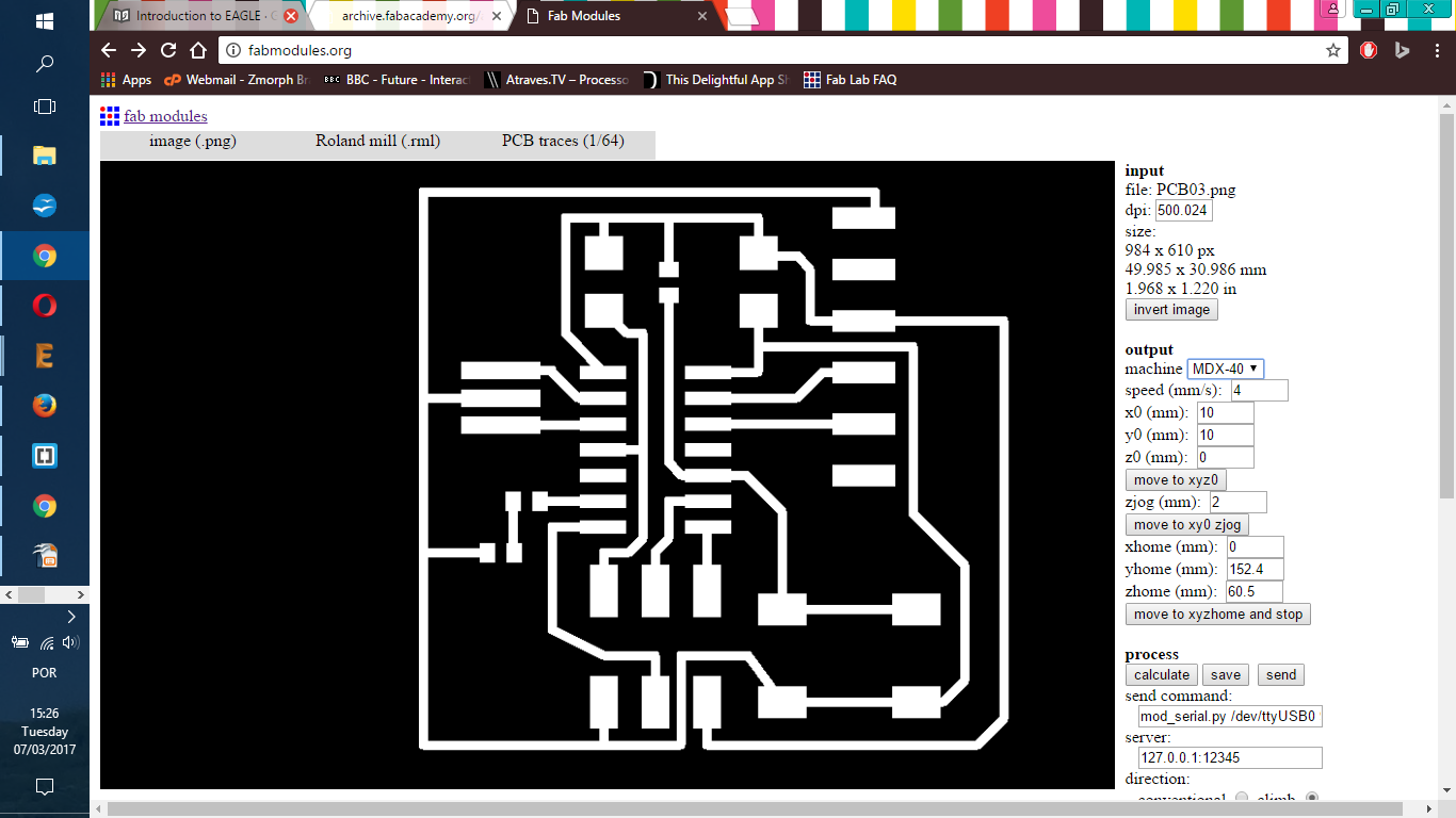
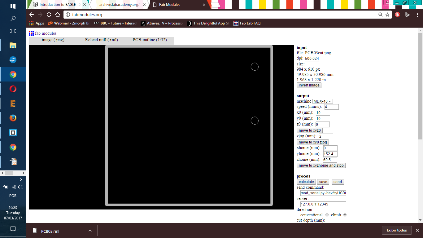
Input: this is an image file png that will describe the traces or cut need on the board. Select the image you need for each PCB. This exercise has this final board design for traces and this final board design for outline.
Output format: Roland Mill (.rml) - this selection will set the FabMoludes to work with a milling machine.
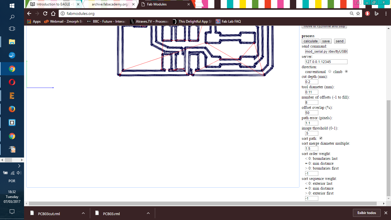
Process: if the selected option is 'PCB traces' than
--- Machine = Roland MDX-40A
--- x0 (mm) = 0
--- y0 (mm) = 0
--- cut depth (mm) = 0.2
--- tool diameter (mm) = 0.11
--- number of offsets = 8
--- offset overlap (%): 50
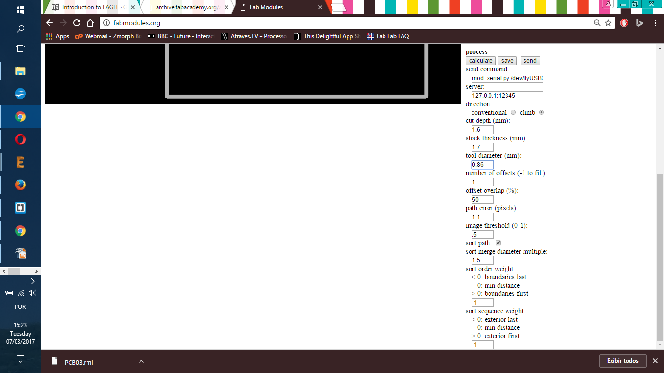
Process: if the selected option is 'PCB outline' than
--- Machine = Roland MDX-40A
--- x0 (mm) = 0
--- y0 (mm) = 0
--- cut depth (mm) = 0.2
--- stock thickness (mm) = 1.7
--- tool diameter (mm) = 2.00
--- number of offsets = 1
You may adjust the setup once you have different milling tools. As the phenolite paper changes from batch to batch, there is the need to compensate ondulations and assimetry eventualy.
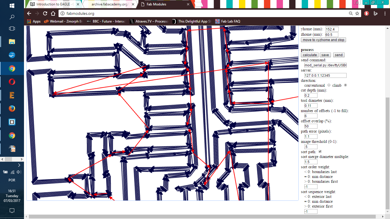
PRESS: "Calculate" button to check how the simulation goes on your computer. Observe if the mill process remove material where it is supposed to and leave material untouched the same way.
PRESS: "save" button in order to have the rml file in your computer.
FabModules allows its user to make other specifications and different setups. I only made reference to the ones needed for PCB milling. Anyother setup may be left the way it comes preseted.
Once the rml program is done, there is the need to move from computer setups to machine operation. Roland's Vpanel program is part of machine's manual (click here); some extra information is displayed below.
The machine needs to be power on in order to comunicate with Vpanel software.It follows some images of Vpanel Operation to config a new job.


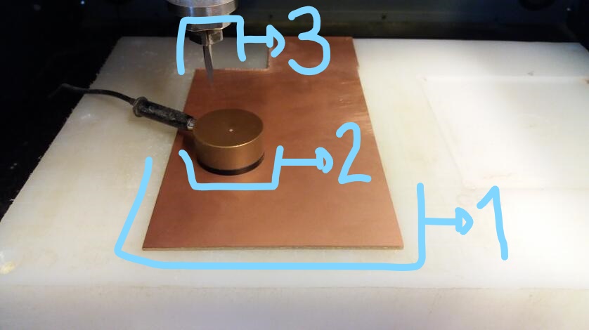
Phenolic paper - copper layer for circuit boards - standard 1,7 mm thickness - example here.
Mill - engraver - 20°edge - example here.
Mill - endmill - 2,00 mm cut diameter - 02 flutes - example here.
"Getting a BOM from EAGLE" tutorial, click here. This is a very old tutorial and its only help was to introduce me to ULP options in FILE menu (besides a smile while reading command line instructions).
From any Schematic in Eagle, you may click 'File' menu and select: Run ULP. This wil open another window with a big set of extra programs. One of them (the first listed in my computer) was called: BOM. Click 'BOM' and then Open button. It follows some ways to visualize or save the information. You'll see bellow the html version saved.
Partlist exported from HelloBoard schematic file.
| Qty | Value | Device | Package | Parts | Description | PROD_ID |
| 1 | 6MM_SWITCH6MM_SWITCH | 6MM_SWITCH | S1 | OMRON SWITCH | ||
| 1 | 6_PIN_SERIAL_TARGETRA_SMT | 6_PIN_SERIAL_TARGET_SIDE_RA_SMT | J1 | 6-pin header connection for use with the "FTDI BASIC" pinout - TARGET SIDE. | CONN-08971 | |
| 1 | LED1206 | 1206 | U$3 | |||
| 1 | RESISTOR1206 | 1206 | R1 | |||
| 1 | UNPOLARIZED_CAPACITOR1206 | 1206 | C1 | unpolarized_capacitor | ||
| 1 | 10000 | RESISTOR1206 | 1206 | R4 | ||
| 1 | 499 | RESISTOR1206 | 1206 | R5 | ||
| 1 | ATTINY44-SSU | ATTINY44-SSU | SOIC14 | IC1 | ||
| 1 | AVRISPSMD | AVRISPSMD | 2X03SMD | U$1 | ||
| 1 | RESONATOR | RESONATOR | EFOBM | U$2 |
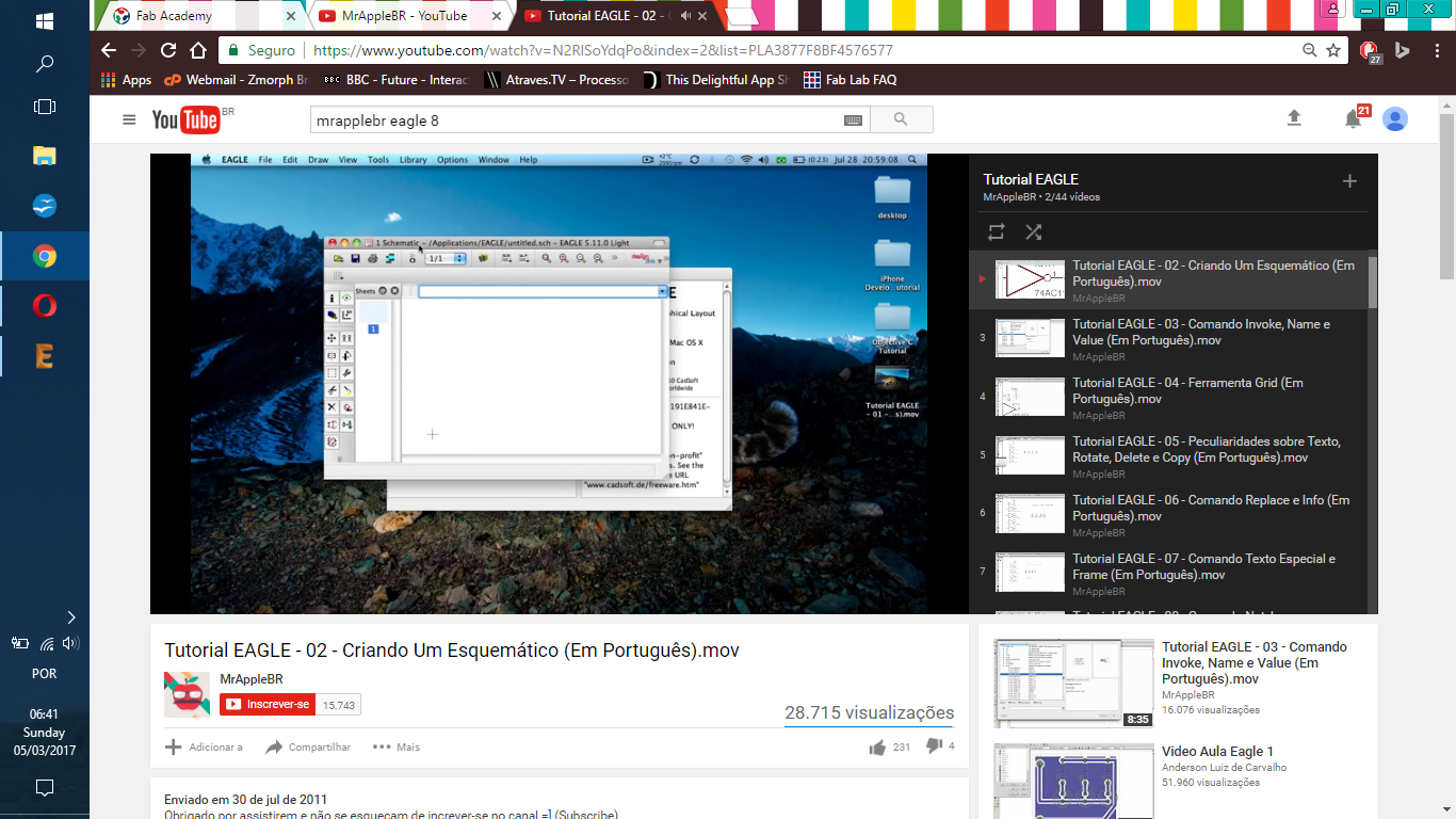
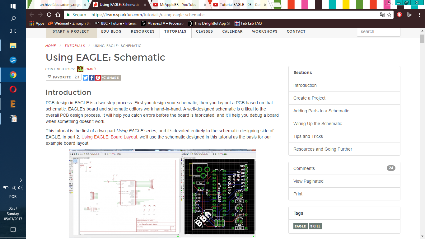
Eagle 8.0 is the Autodesk version of this software. There was the need to adapt tutorial's intructions. Tutorials were made for Eagle 7.0. The main issue was to find components in the libraries. It took me a while to find the way and get the tutorial done. I starter with MrAppleBr's tutorial, then FabAcademy first tutorial list and finish with the Hello Board schematic and PCB.
As expected I did somethings wrong and had to fix the PCB design and produce more than one prototype. This process was important to learn better where to find information about components and how place them over the PCB surface.
.bmp)
.bmp)
.bmp)
.bmp)
.bmp)
small.bmp)
small.bmp)
small.bmp)
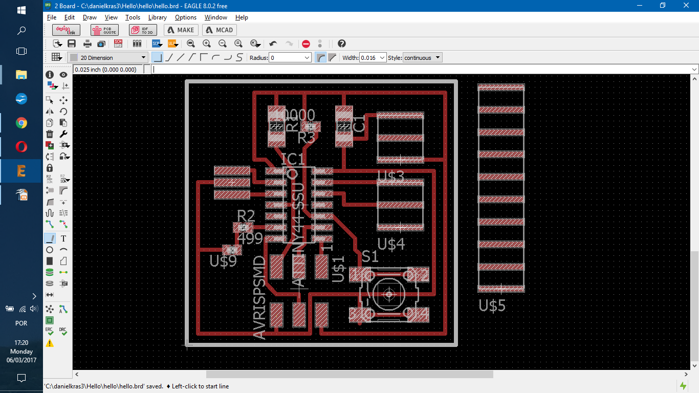
In order to get a PNG file from Eagle follow this instructions:
- Click Layer Settins;
- Click None - this will clean full selection.
- Click the numbers representing traces layers - #1; #16; #17; #18.
- Click OK.
- Click File/Export/Image.
- Search the place you want to save the file - click Browse...
- Select Monochrome.
- Set Resolution to 500dpi.
- Click OK.
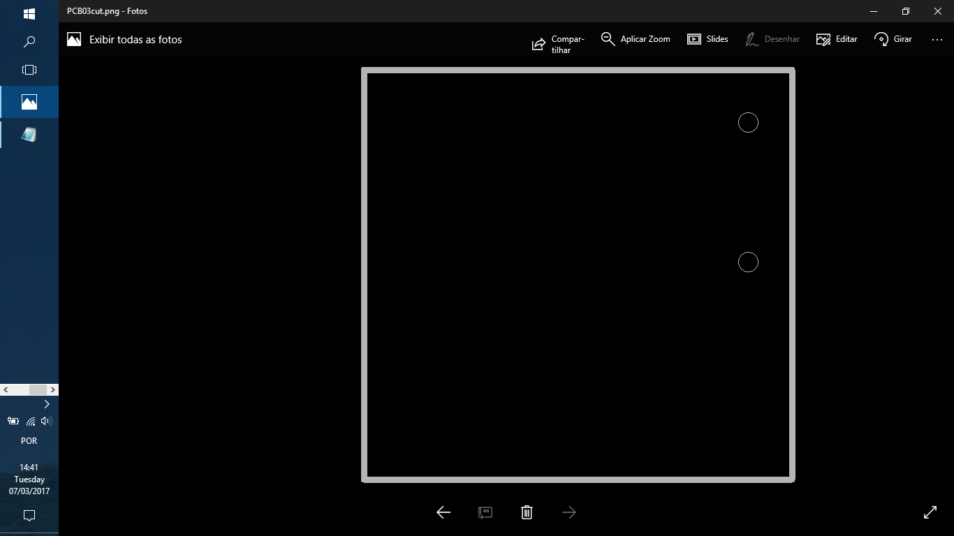
- Repeat the instruction but change layer settings to only layer: #20.
With this two images is possible to create traces and cut files from the design to production machine code.
The documentation of Raphael Schaad is really nice and is suggested during the weekly lesson. I will complement my documentation with a quote of his vocabulary list. I tried to find his contact to write him an e-mail letting him know about my quote, but his webpage has no contact info.
-----------

This work is licensed under a Creative Commons Attribution-ShareAlike 4.0 International License.