What's Electronics Design
Two weeks ago, we were talking about Electronics production to fabricate a pre-designed circuit. This week we are focusing more on the designing process. The designing process start from drafting the circuit on paper, then desiging a schematics that shows how components are legally connected. Then designing the board layout, or PCB layout, that shows how the components are organized on the actual board. When you finish designing, you have to export your design to be fabricated.
Step 1: Setup your Environment
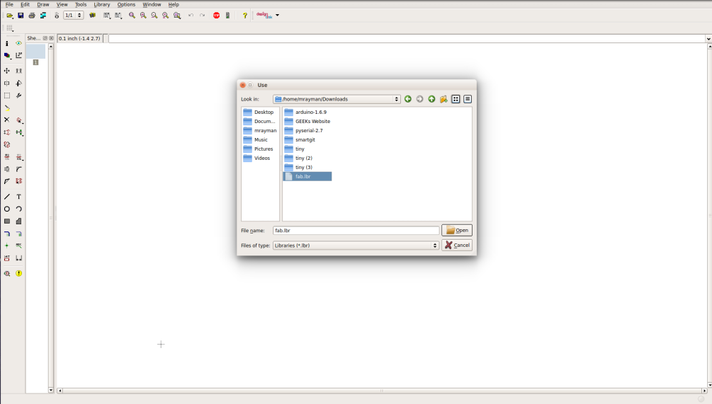
This week we are using Eagle software to design our circuit, you can download it here. Then after installing your software, you will have to download the fab library that contains all the components we will use. You can find it here. Just search for "fab.lbr". When you download the file, you can move it to your sketchbook director, inside lbr folder. Or you can just click on "library" then "use" and browse for the library and click ok.
Step 2: Schematics Design
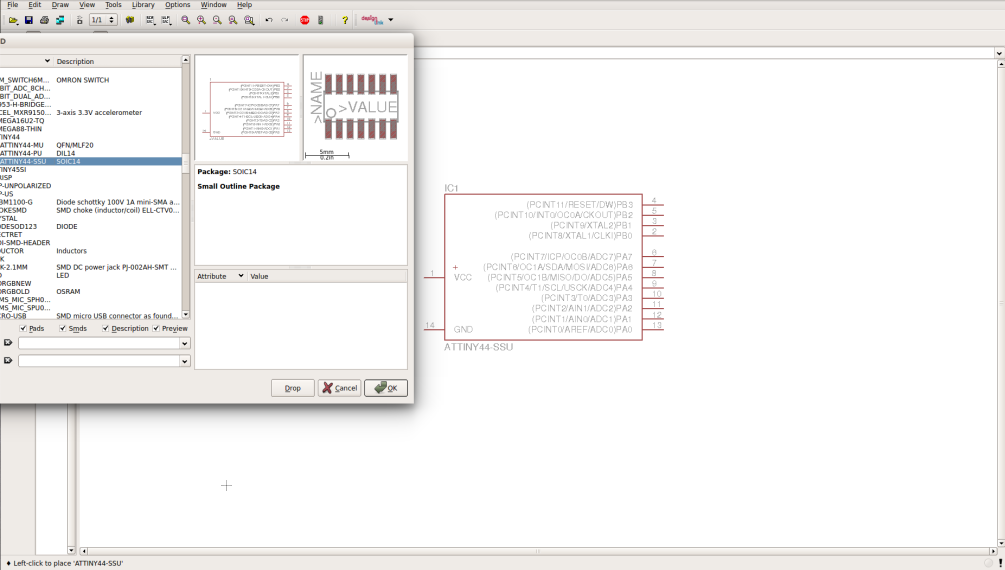
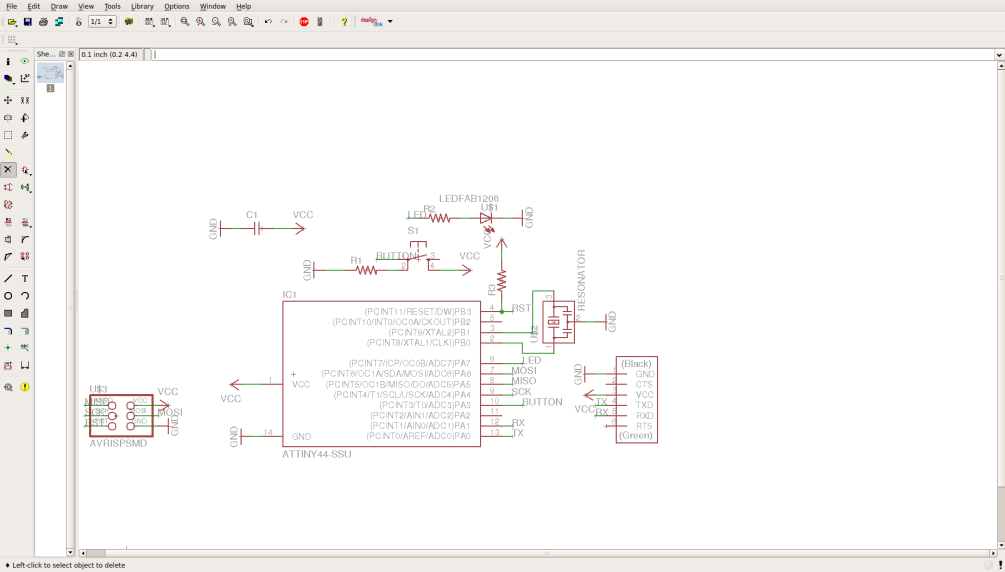
Start a new project, then create a new schematics (.sch) file. Now it's time to start adding your compoentes. You may use the hello world circuit as a start point, but you gonna need an extra led and button. Add all the componets needed and keep them apart. Remember to choose the right pacakage of compoenents, becuase each package has its own dimensions, and if you have picked the wrong one you will not be able to solder the components.
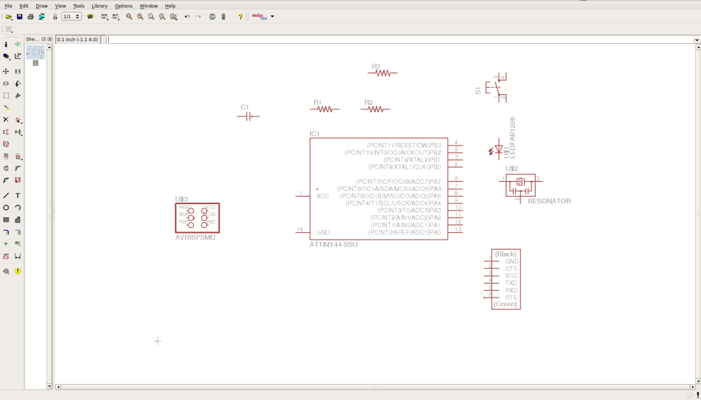
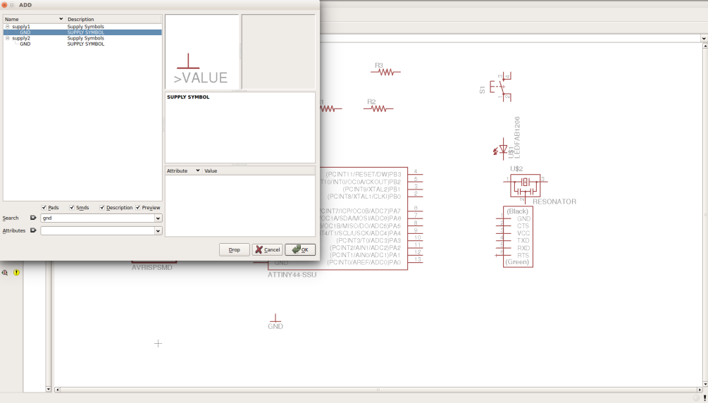
Then it's time to start wiring, you have to connect the components together in a legal way so the software can understand how the circuit is connected in order to be able to design the PCB layout. There are a couple of notes that you will need to know: 1. Don't connect components using the wire tool, only use "net" tool. 2. If you are not keyboard oriented, use a mouse, don't use touch pads. 3. Instead of literally wiring everything together, and ending up with a messy circuit. You better just name the pins and if you want to connect two pins just name them with the same name. 4. Don't forget to save your file from time to time. 5. Use "Gnd" and "vcc" symbols to simplify your circuit.
Step 3: Routing (PCB Layout)
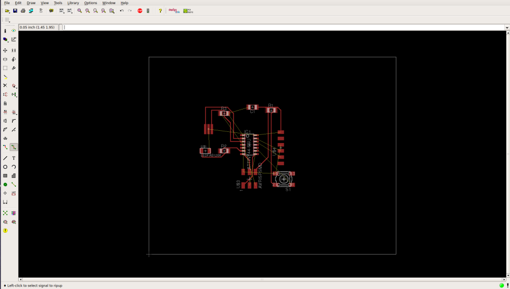
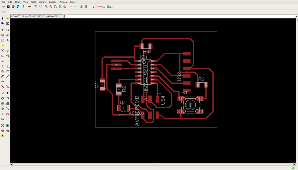
When you finish wiring your circuit, just click on "generate/switch to board view" button on the toolbar. I have used the autoroute tool, and I removed the connection in the other layer. And after some editing I finally got it.
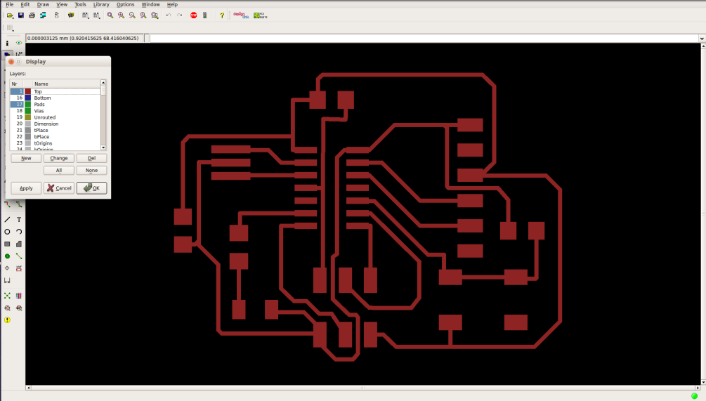
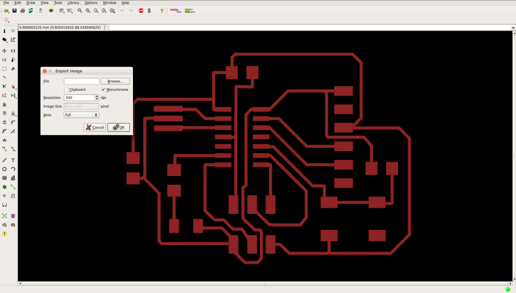
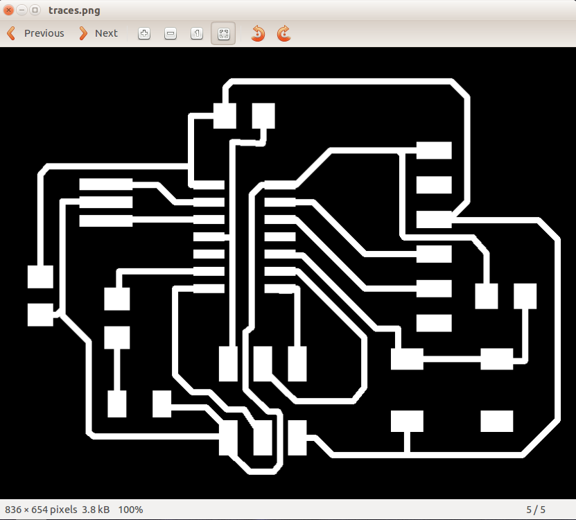
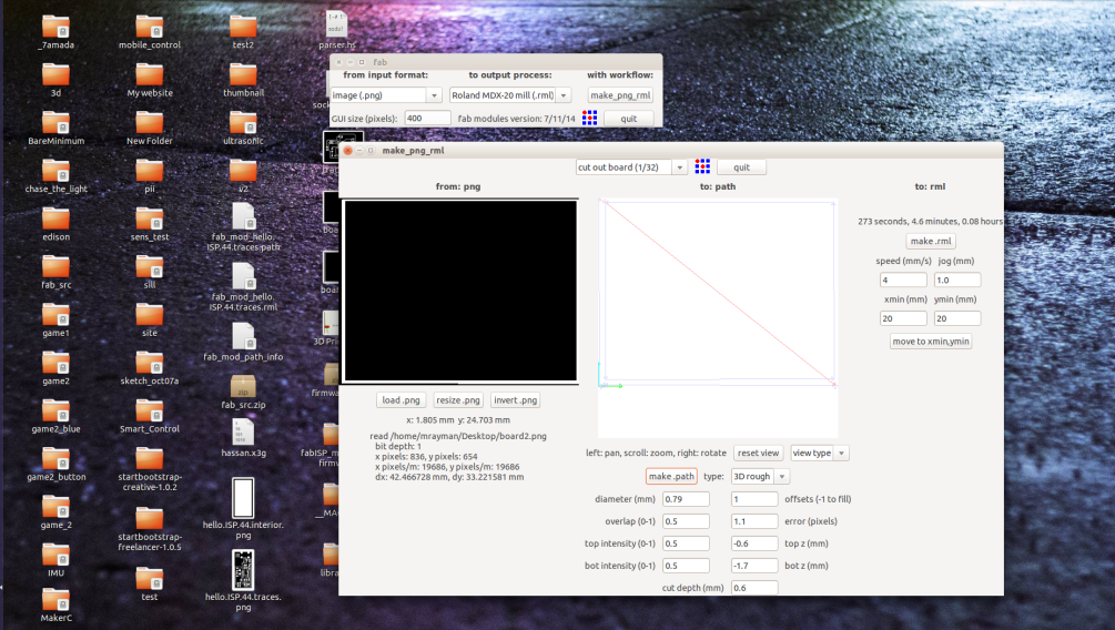
Now it's time to export our design. First we only need the layers of traces and pads, so from layers menu uncheck everything and only keep the top and pads layers. Then export to image, the resolution -in dpi- is important so the machine can read the dimensions right, I use 500 DPI for the MDX-20. Keep you image to monochrome to get a black-and-white image. Remember we need to files to manufactur the circuit, traces and boarder image. So after exporting the traces, re-open the layers menu and only keep the dimensions layer, and export another image.
You might need to enlarge the border line so the fab modules can see them, use Gimp, paint, or photoshop to do this.
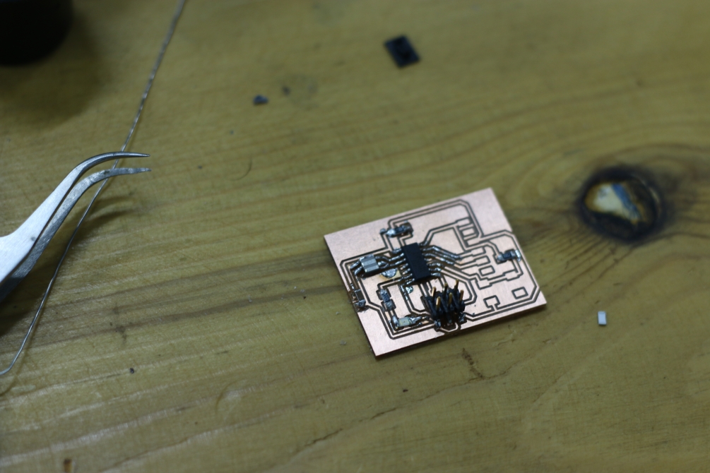
Step 4: Making the board
I guess you became familiar with this process now, if you need a more extensive documentation check my pervious asignment Electronics Production.
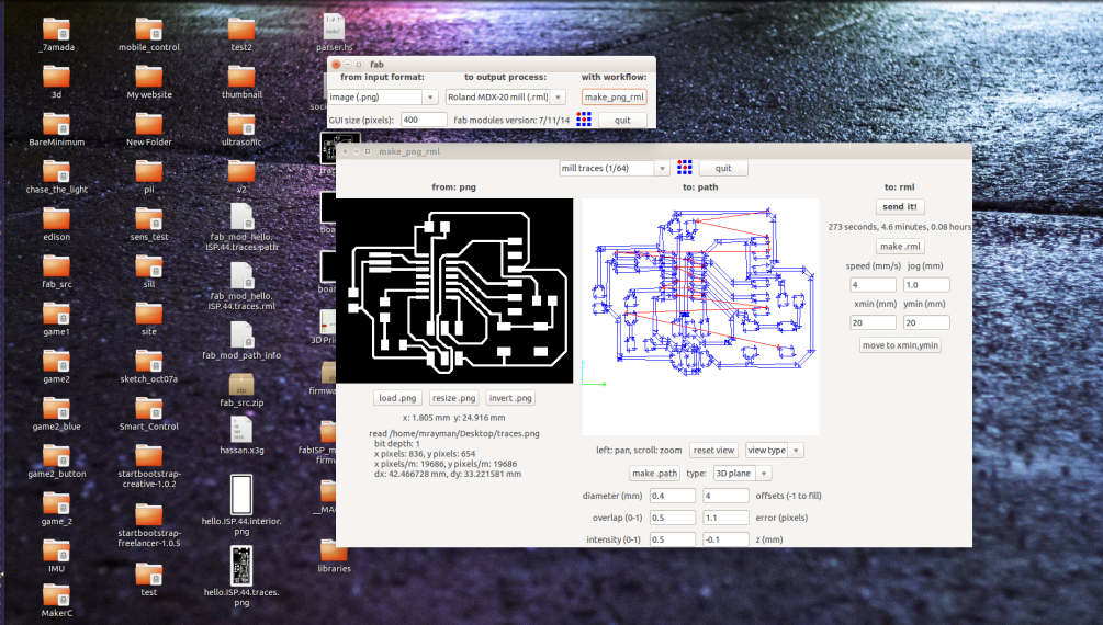
Load the images to the fab modules, adjust your parameters, zero z-axis, and then start milling.
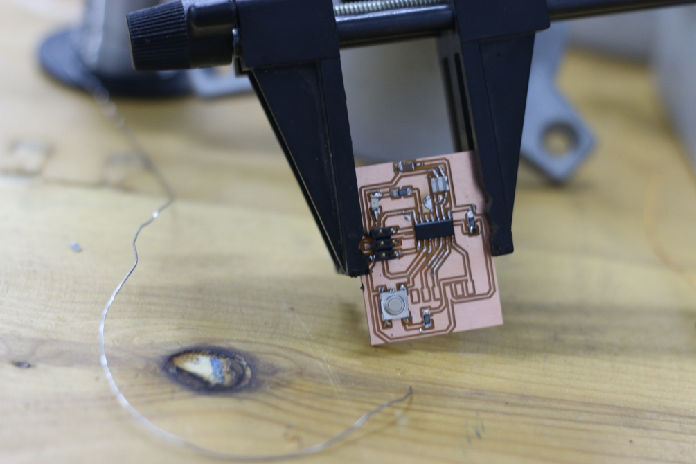
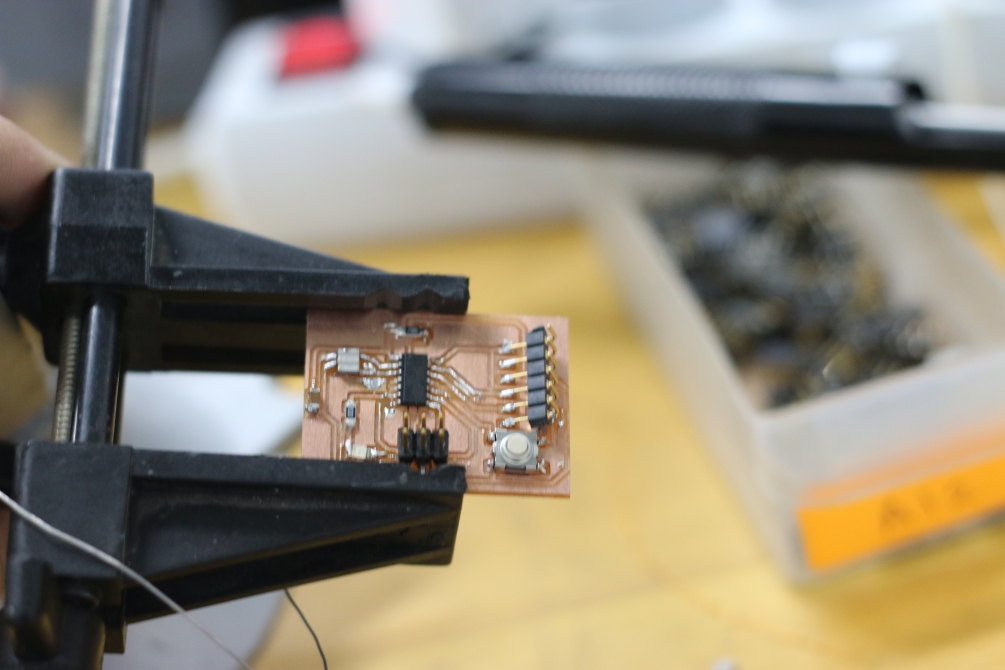
Step 8: Soldering
This week it's easier for me to solder, practice makes perfect. I had a little difficulity soldering the resonator, as it has no pins or pads. But I find an easy way to solder such a component. All what you need to do is to add some solder to the pads, then using a tweezers hold the component on the top of the pads (on which you have added solder), and then use a hot air to melt the solde and gently push the component downward to sink in the solder.
Step 9: Programming the board
We will take about this step in the after next assignment Embedded Programming.