- Week 13 +
input devices
Tasks
Introduction
For this week’s assignment, I have decided to use a button as my input sensor as it is relevant to my final project. The button is used to detect physical compression. The button can be physically replaced by two metal plates, which, when brought into contact, will register as the closing of a switch. This is just an example.
Here are the steps that I used to create the input device using button:
Workflow
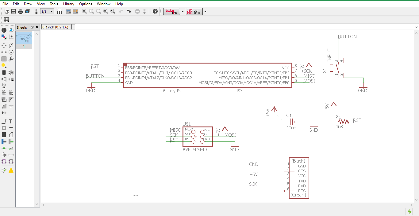
Step 1: Adding components to schematic
After studying the datasheet of the ATtiny45 microcontroller, I realised that for this board I do not require an external 20MHz clock since precise timing is not an issue here. I designed the board to have an FTDI header so that the pressing of the button can be registered by a serial monitor on the PC.

Step 2: schematic
After adding all the connections and components, the schematic is completed.
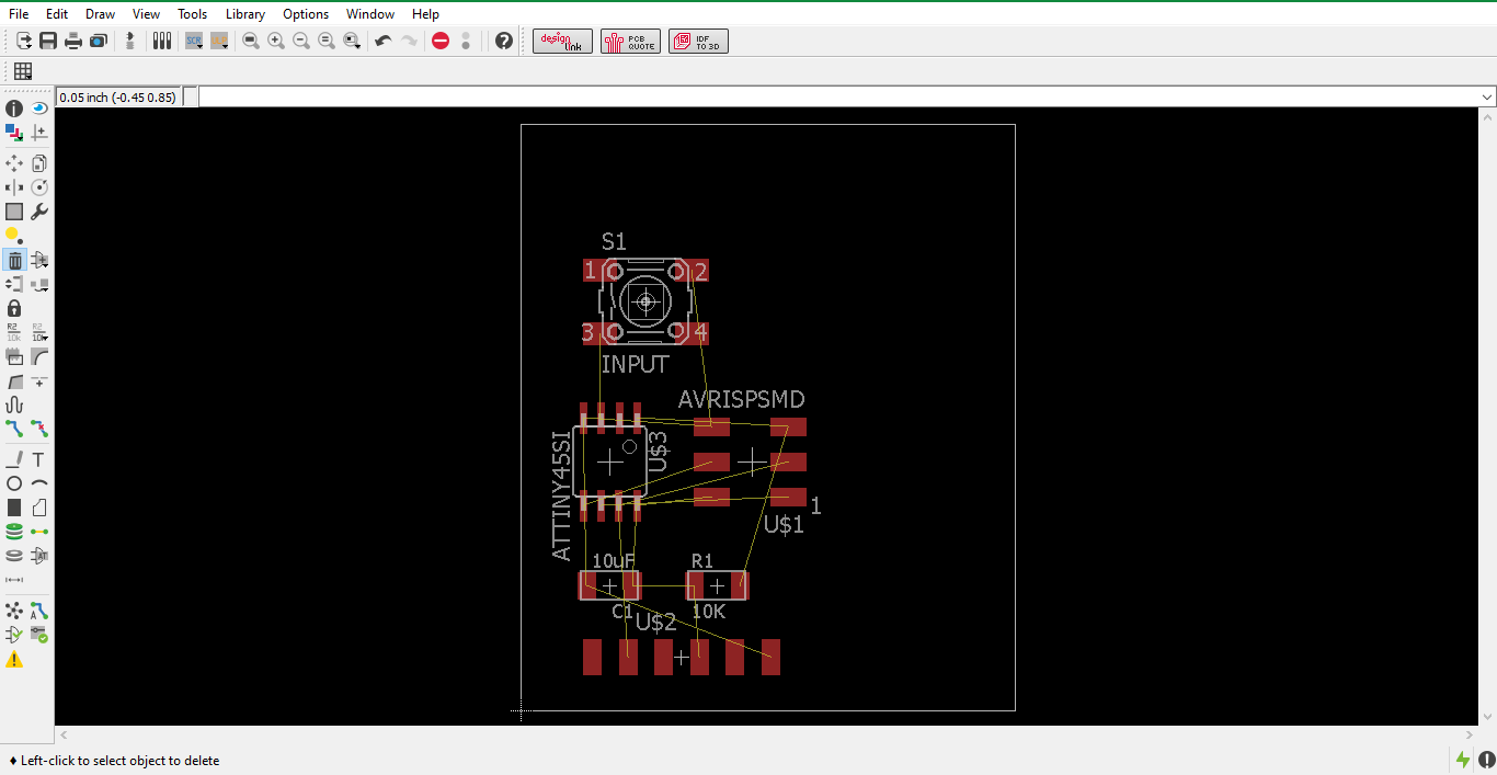
Step 3: Arranging components
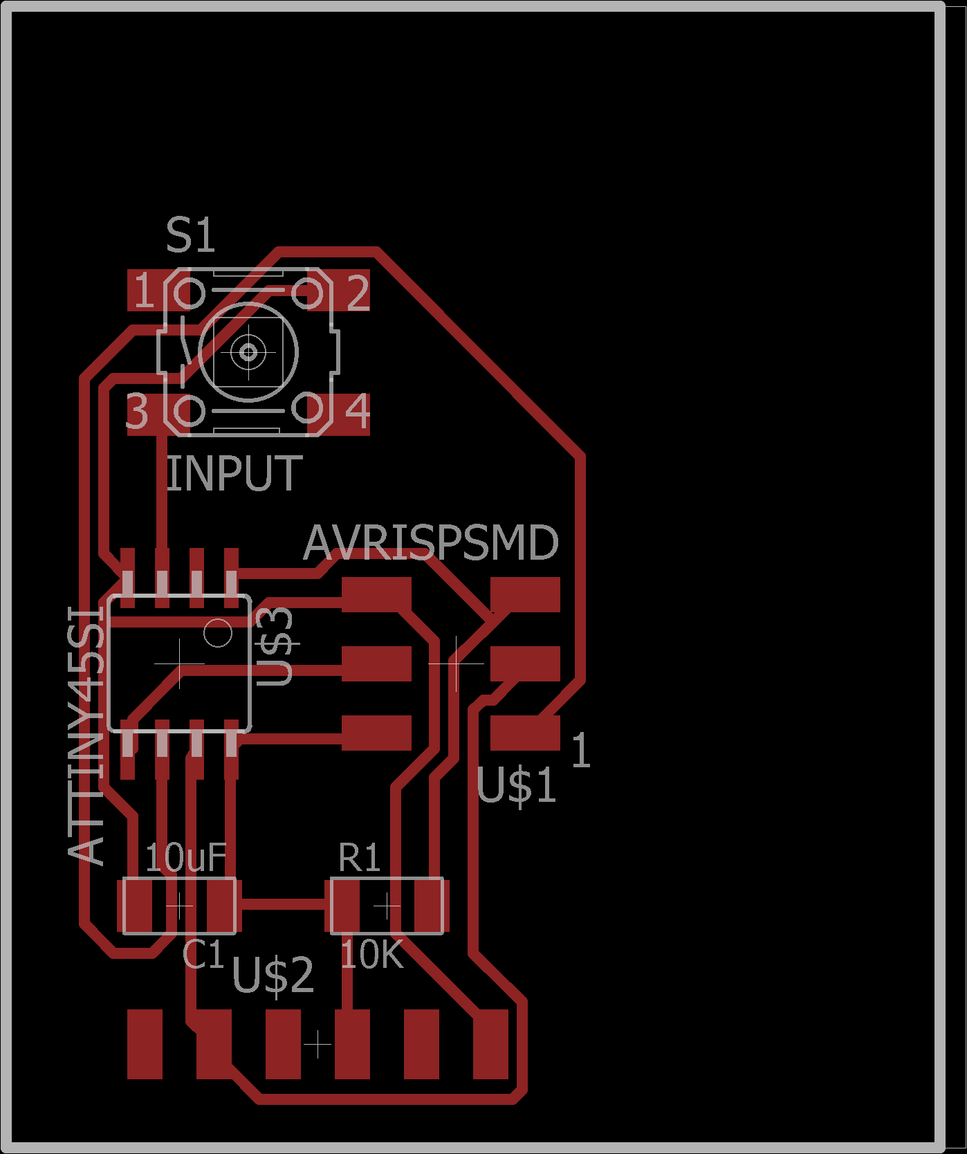
After completing the schematic, the board layout window was opened. Here all the components along with a pcb boundary are shown in this screenshot.
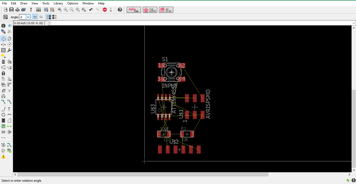
Step 4: Circuit before autoroute
The components are rearranged and the pcb size determined. I clicked on the ratsnest icon in the left vertical toolbar to simplify the ratsnest.
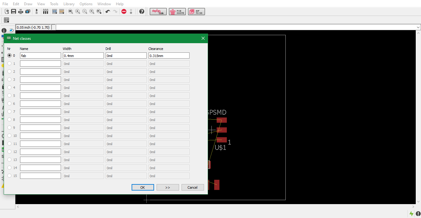
Editing net classes
Step 5: I then edited the net classes with the following settings:
- Width: 0.4mm
- Clearance: 0.315mm
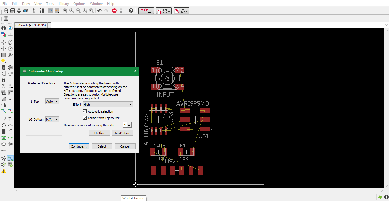
Step 5: Begin autoroute
Now, I selected Autorouting with the following settings:
- Top: Auto
- Bottom: N/A
- Effort: High
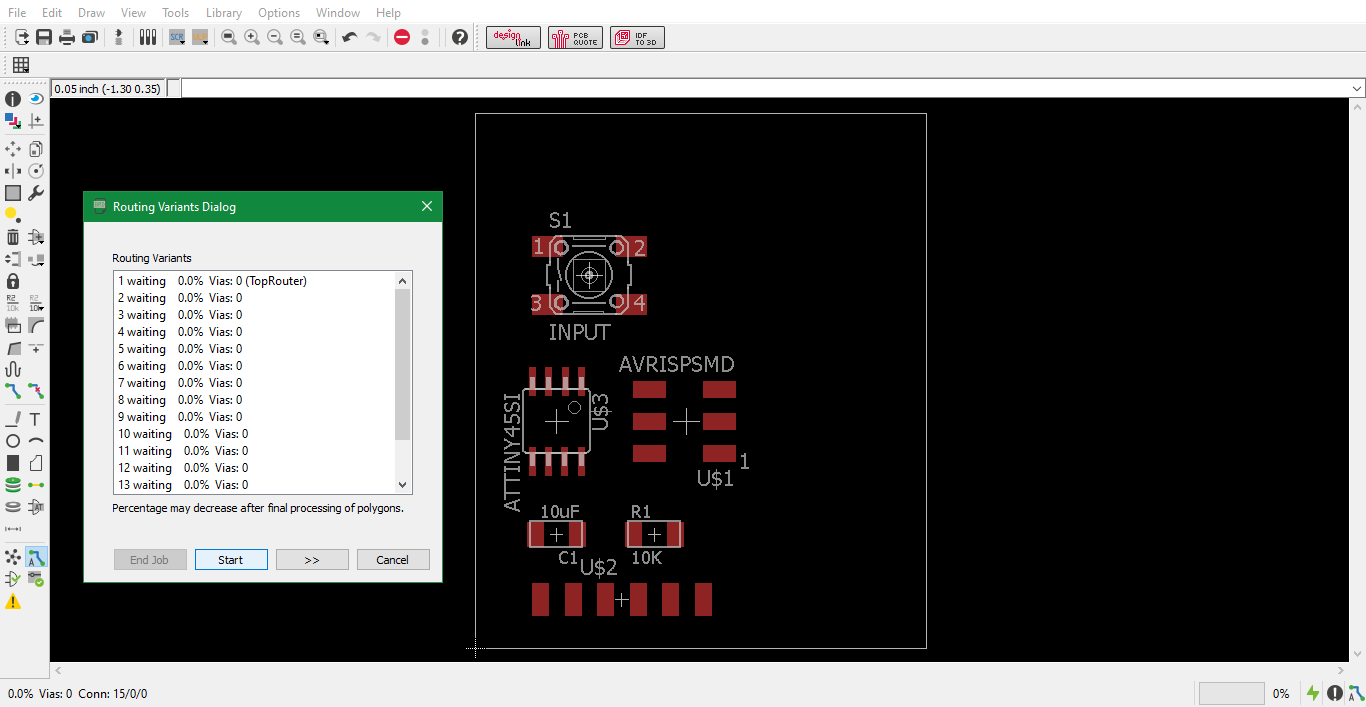
Step 6: Autoroute window
The AutoRoute window shows all the different threads that test different PCB designs.
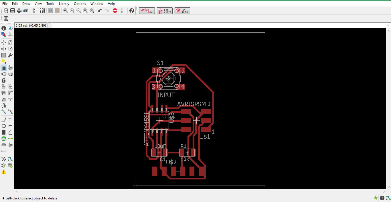
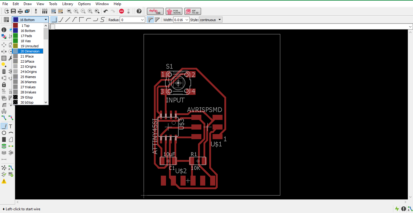
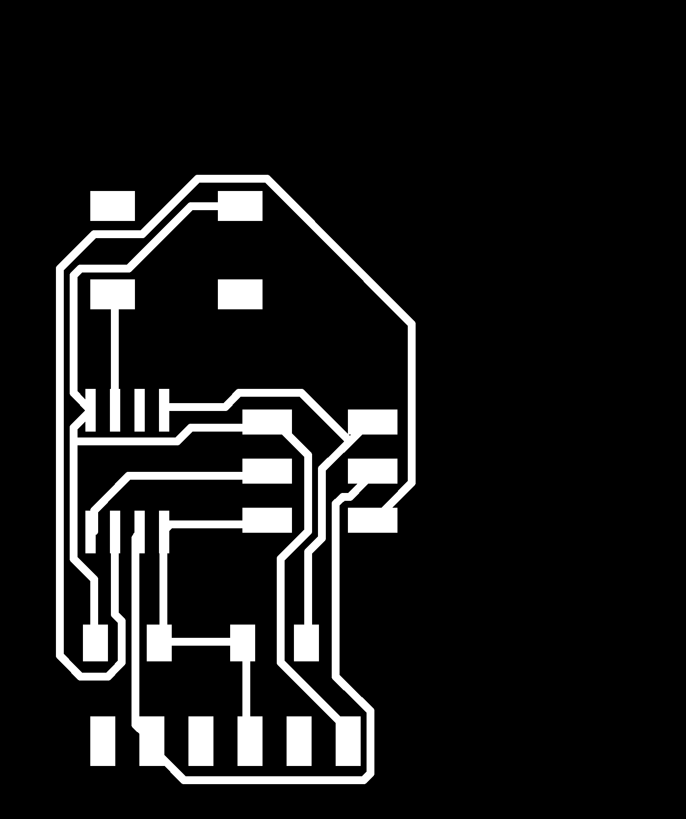
Step 7: Autoroute completes
After completion of autorouting, I chose the best possible design and finalised it.
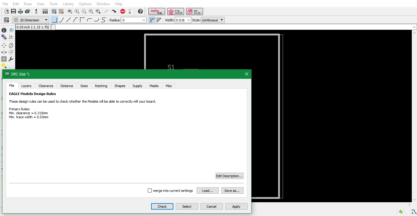
Step 8: DRC check
I verified the design using the DRC. I obtained no errors and proceeded to the next step.
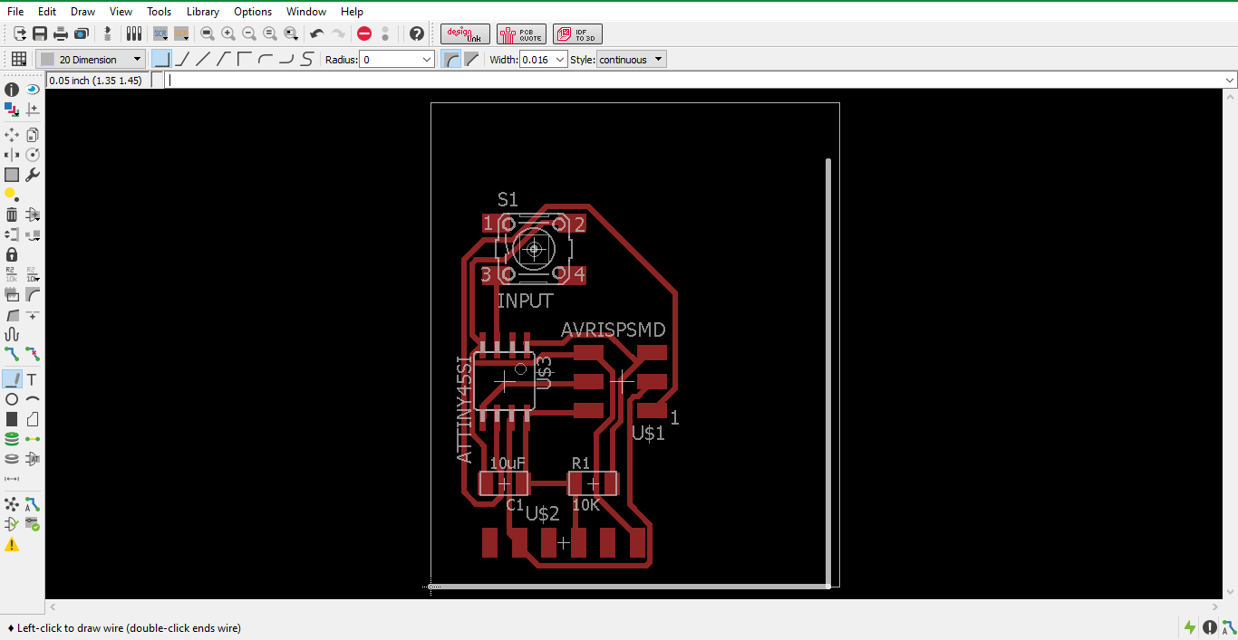
Step 9: Drawing interior
I decided to draw an interior by selecting the wire command and selecting Dimension from the drop down menu as shown in the screenshot.
Step 10: Drawing interior 2
I started drawing around the board traces. This will be the size of my PCB.
Step 11: Layer settings
Now I proceeded to the step for producing PCB fab files. So I selected View > Layer settings… to choose which layer I want to make visible.
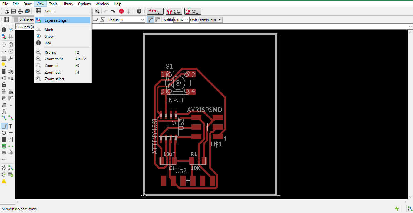
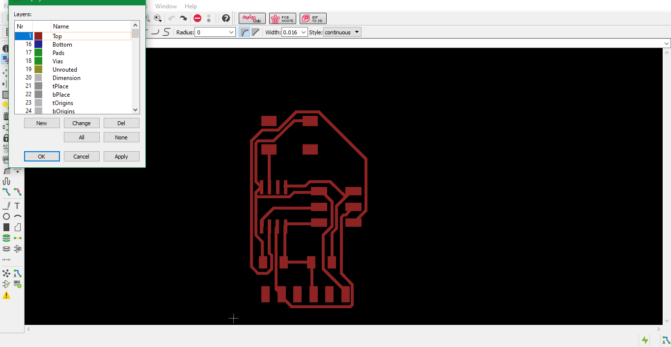
Step 12: Showing traces layer
In the layers window, I first choose the Top layer to display just the traces, and then click on OK.
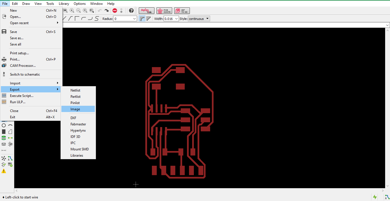
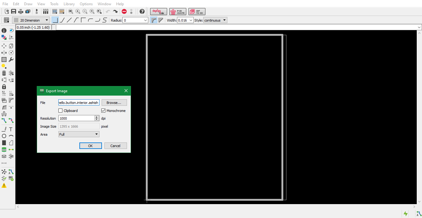
Step 13: Exporting image
Then I went to File > Export > Image to export the image.
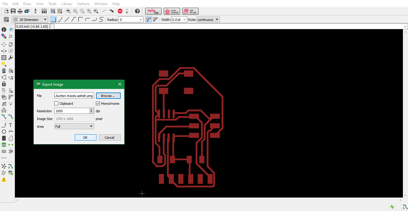
Step 14: Export window
The export windows gives the option of choosing the name of the file, its chromacity and its resolution. For the traces I chose to export a monochromatic image of resolution 1000.
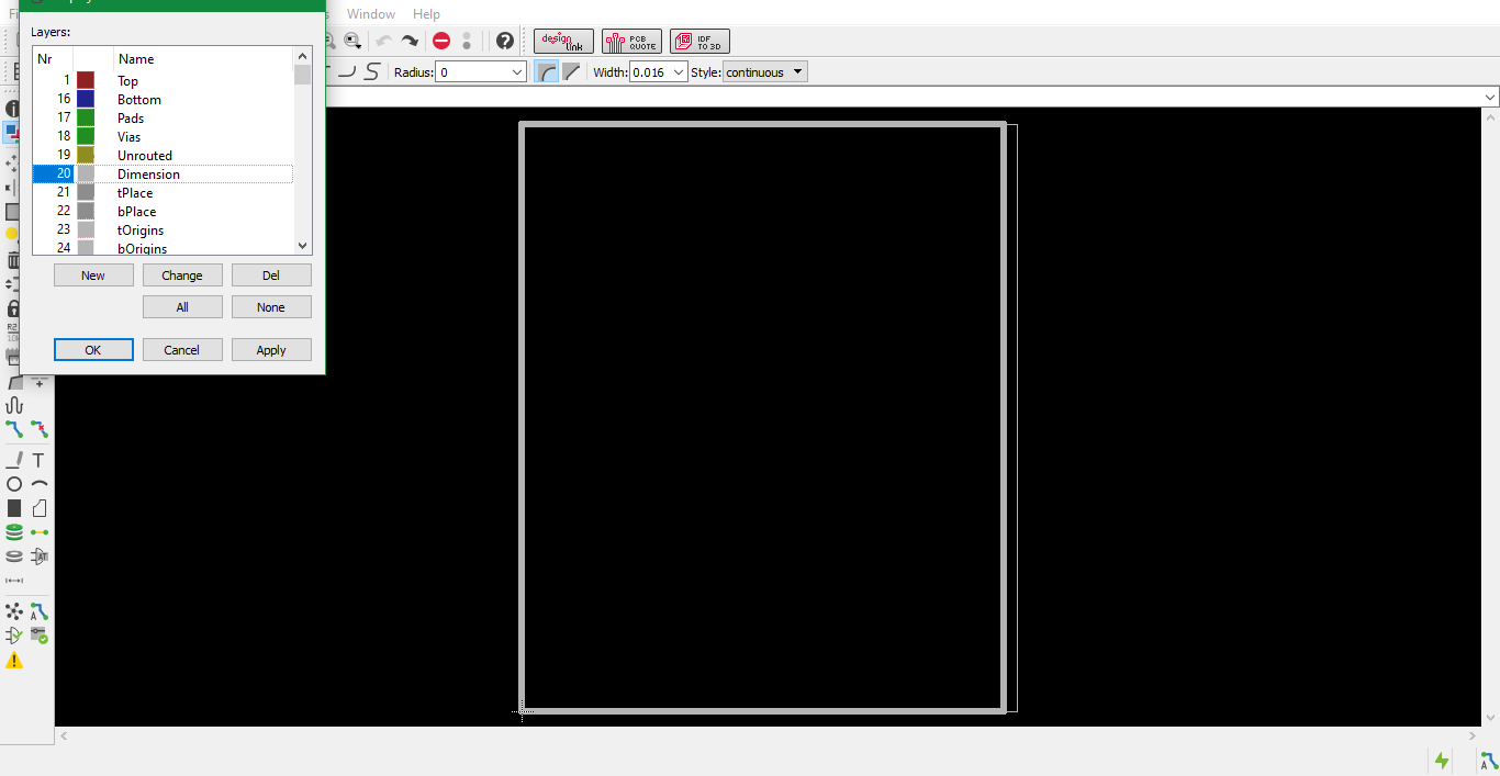
Step 15: Showing interior layer
Similar to step 13, I chose the Dimension Layer and clicked on OK.
Step 16: Export window 2
Then I exported the interior image file like steps 14-15.
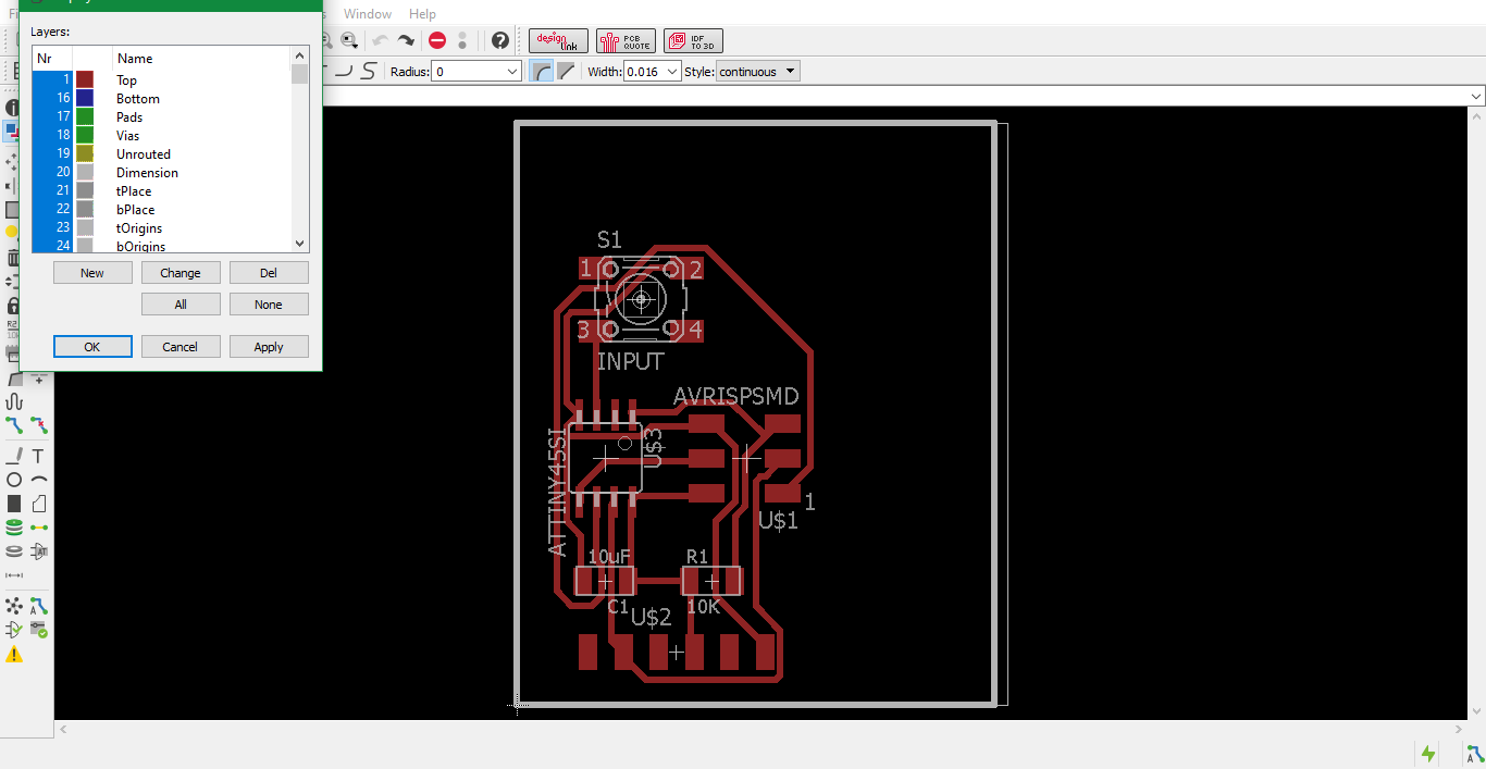
Step 17: Showing all details
Finally, in the layers window I chose all the relevant layers and clicked on OK.
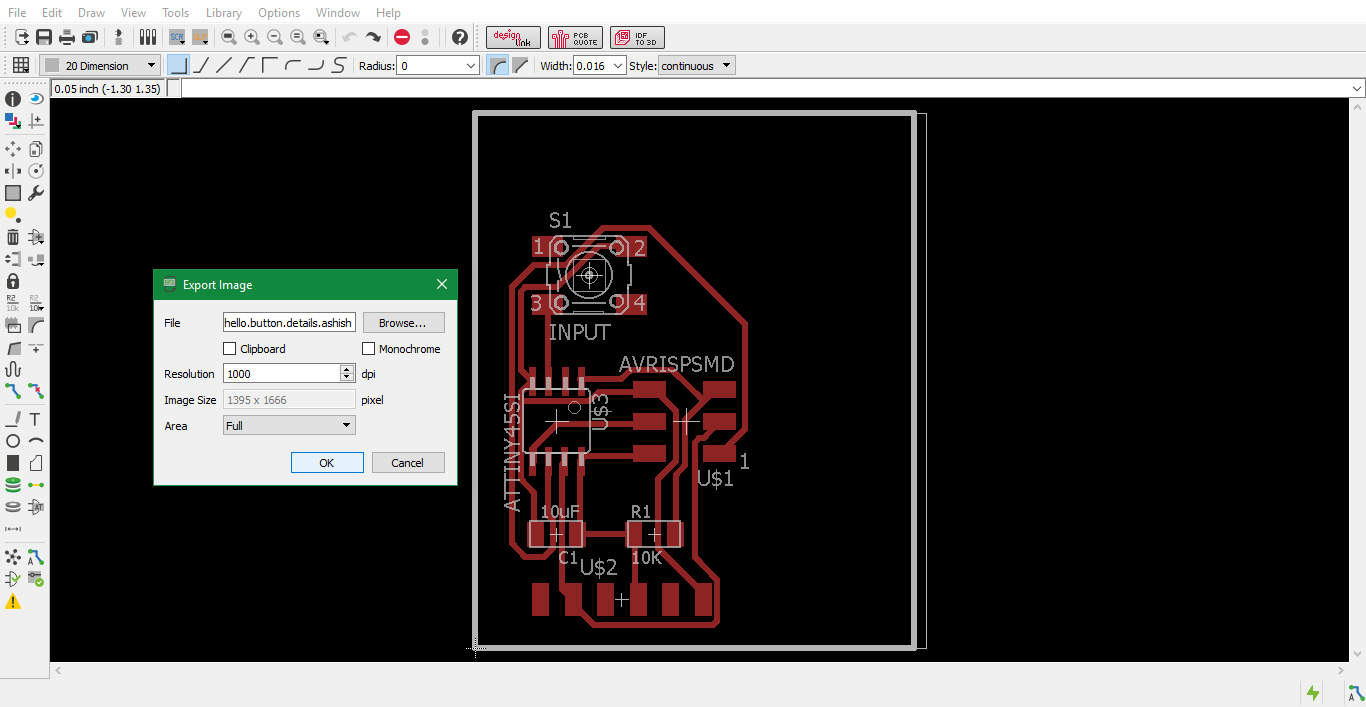
Step 18: Export window 3
And then I exported the image with all the details of the board for future reference.
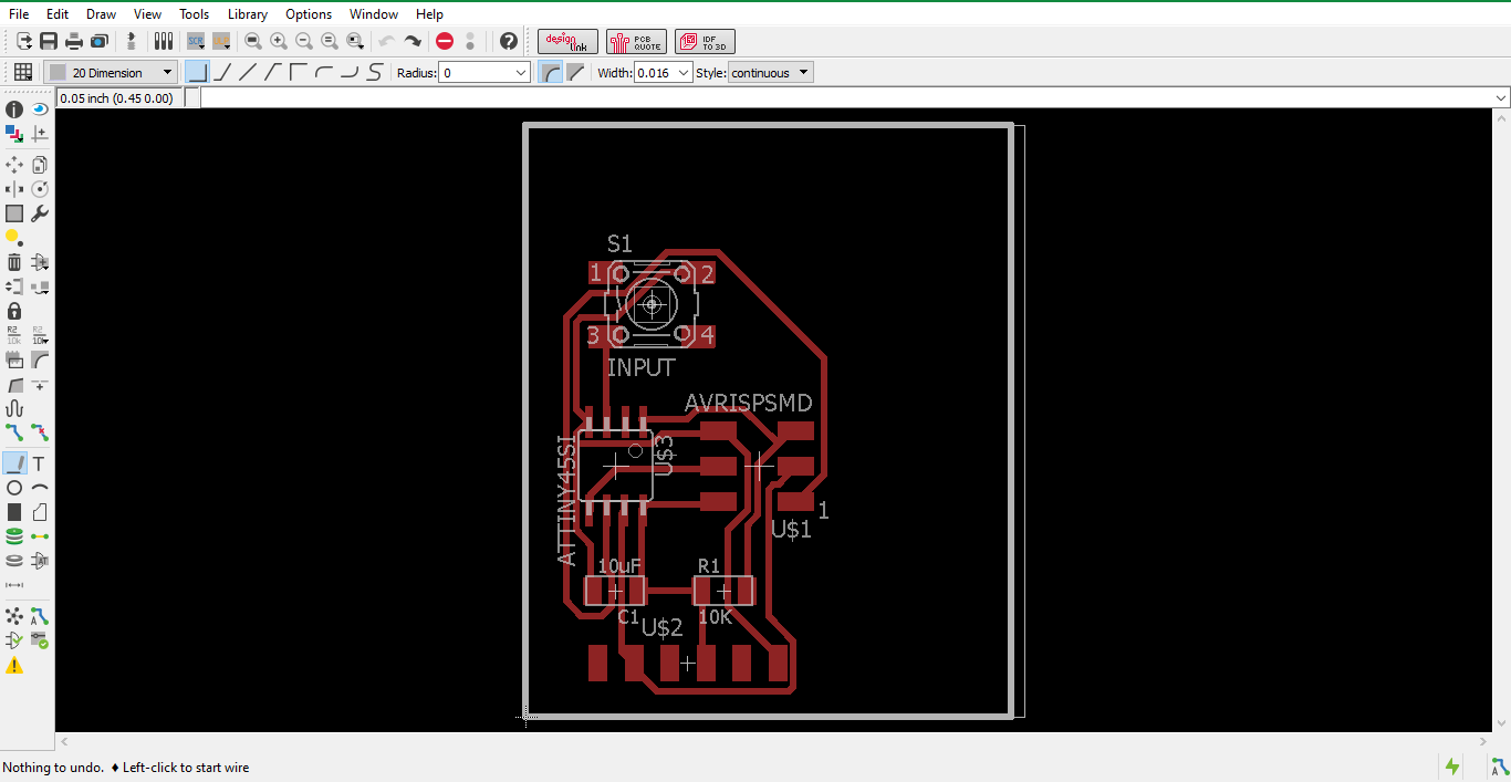
Step 19: Finished board
And with this, our PCBs are ready for production.
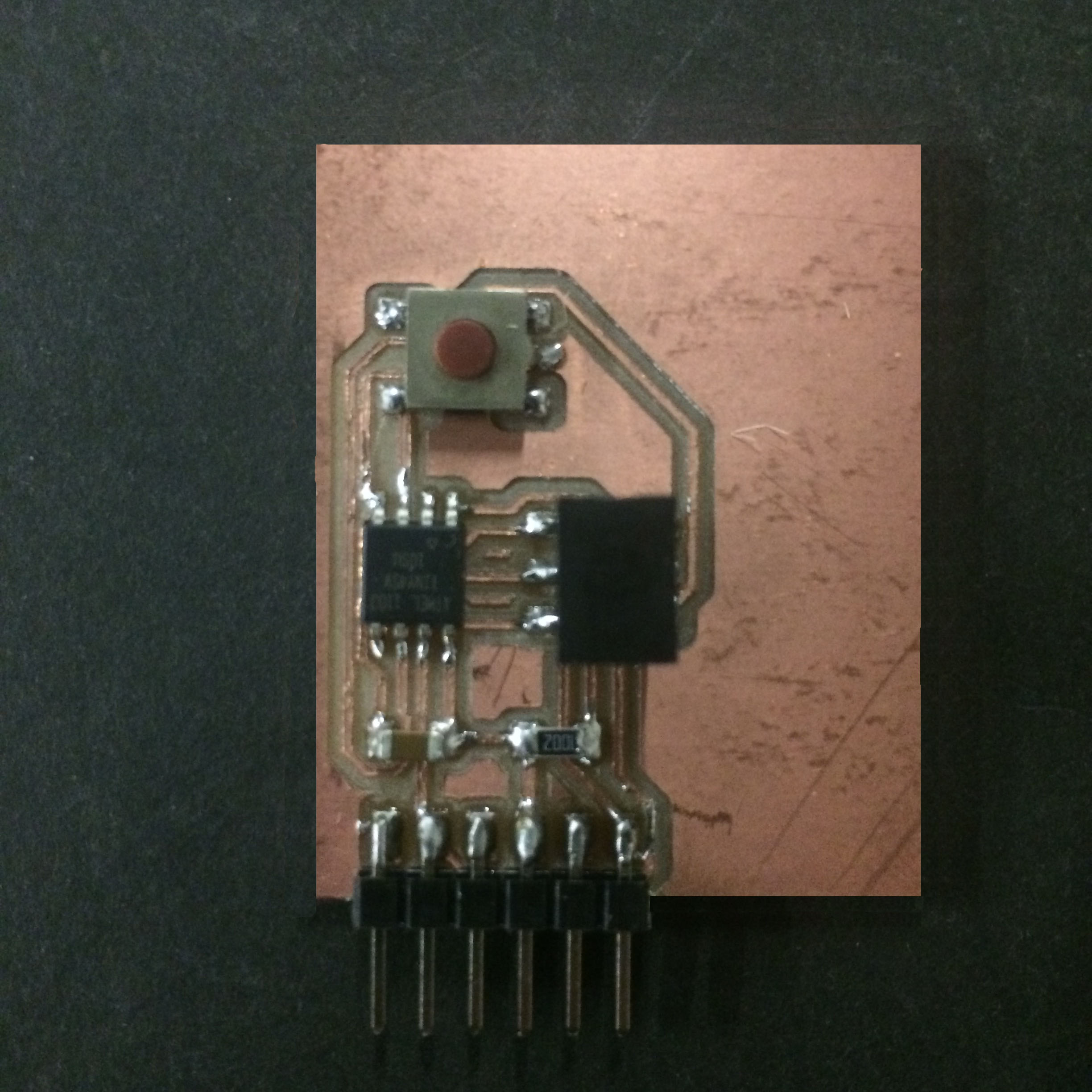
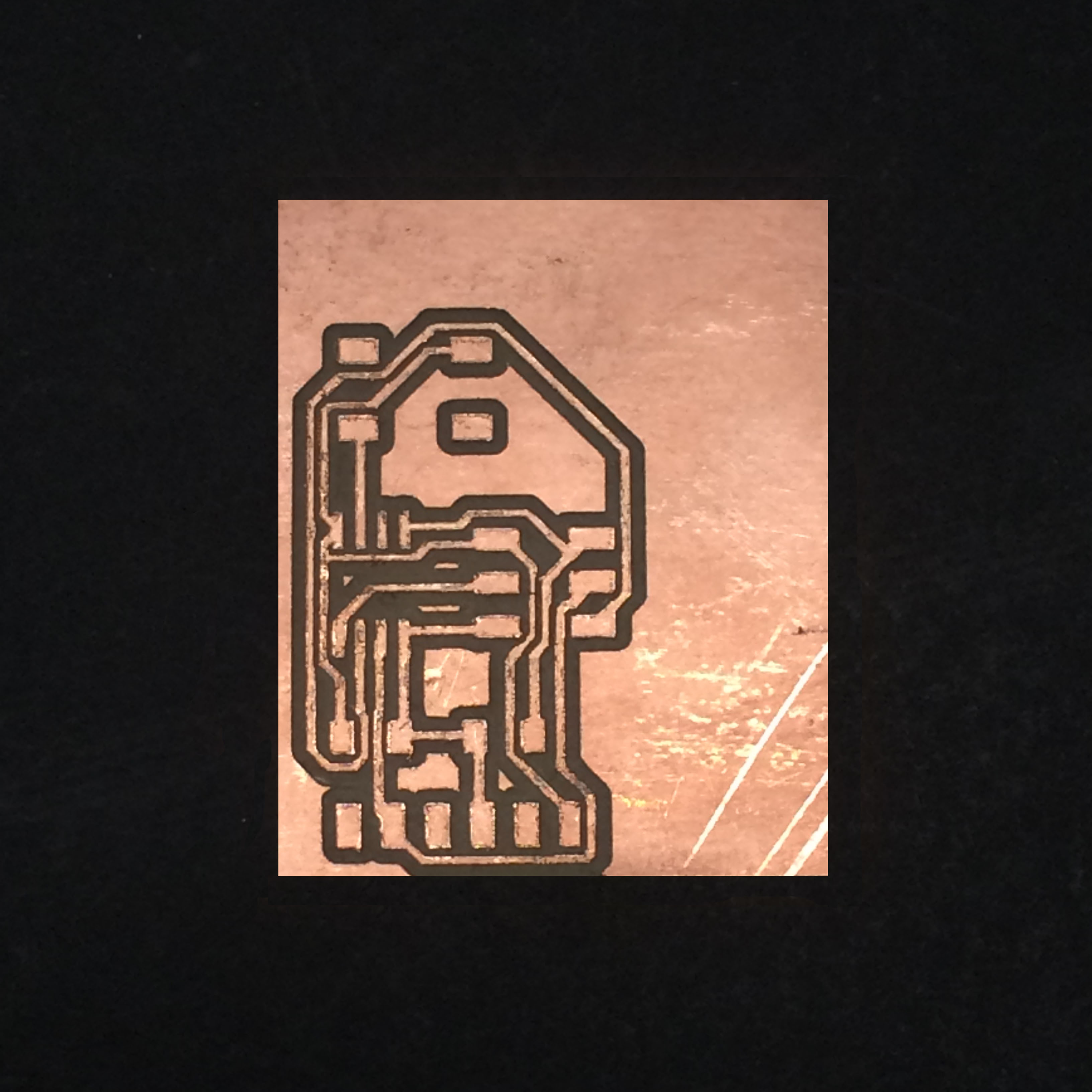
Circuit Board
Programming
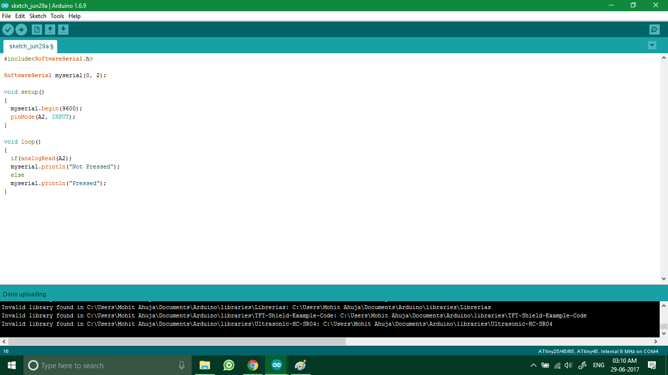
Once the circuit was soldered and ready, I proceeded to program the circuit with the relevant code. For this I wrote a simple code that reads the analog voltage on A2 and displays “Pressed” or “Not pressed” it on the serial monitor by using SoftwareSerial library. This is also a proof of concept that the button can be replaced by other sensors such as a photodiode, a piezo disc etc. The simplicity of the code makes it a modular code, so that one can refer to it as is or add their own custom features.
This program reads the state of the button which is attached on pin number A2. So I began by writing the code.
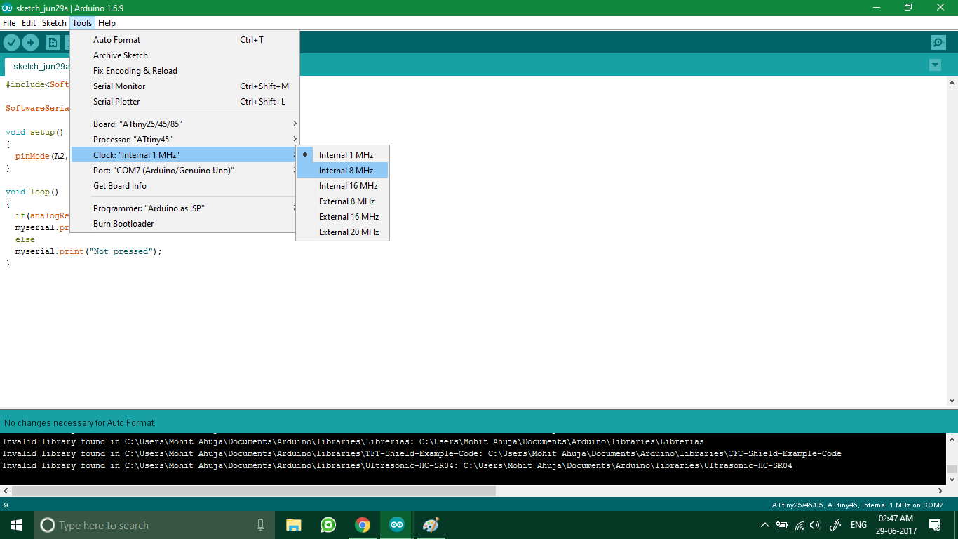
After that, I chose the relevant settings for uploading the code to the board:
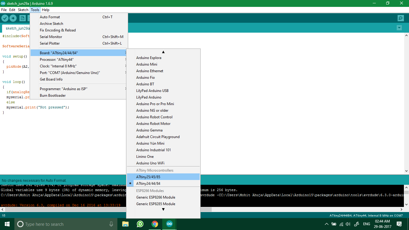
Select the processor - attiny45
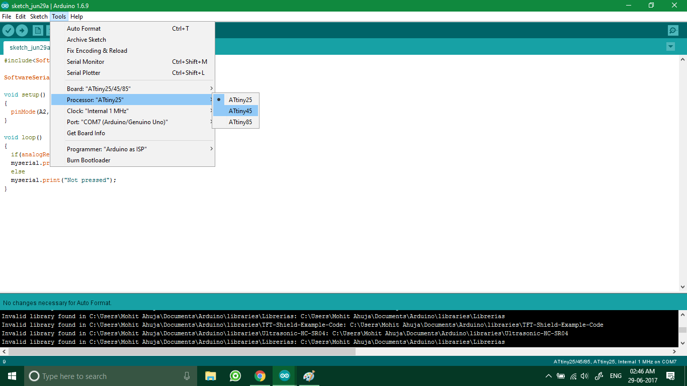
Selecting the clock - 20Mhz external resonator
And finally the result was seen on the serial monitor.
The programmer is an Arduino Uno programmed as an ISP
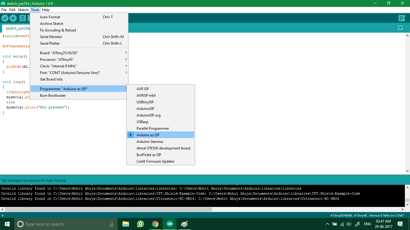
Burning the bootloader burns the arduino IDE's bootloader into the IC
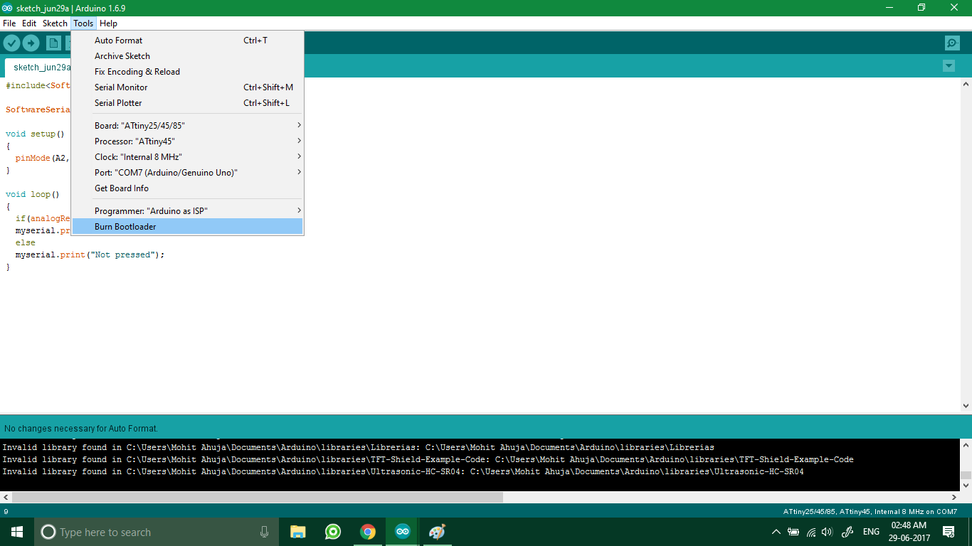
Now I clicked on Burn Bootloader after loading relevant settings. After burning bootloader, I also uploaded the code.
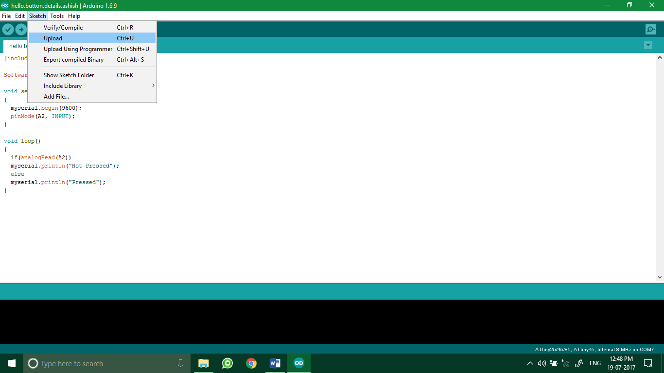
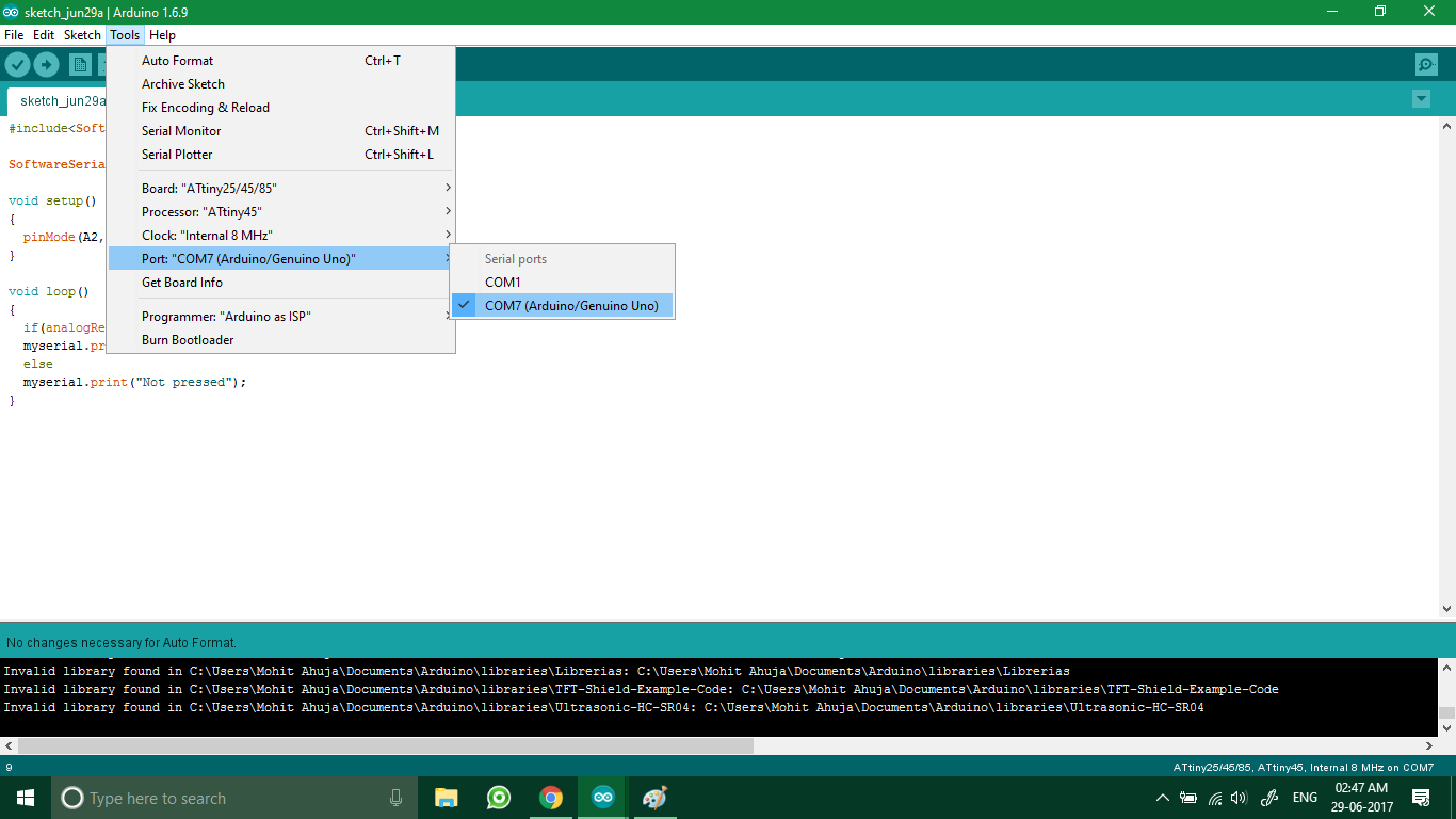
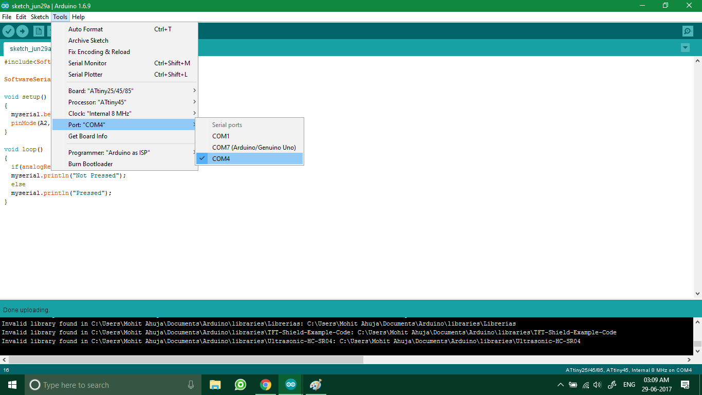
This board is programmed via Arduino as ISP, but its result will be available on the serial port. So once the board is programmed, I changed the port to the FTDI cable’s port.
Code
#include<SoftwareSerial.h>

SoftwareSerial myserial(0, 2);

void setup()
{
  myserial.begin(9600);
  pinMode(A2, INPUT);
}

void loop()
{
  if(analogRead(A2))
  myserial.println("Not Pressed");
  else
  myserial.println("Pressed");
}
Demo video
The video demonstrates the program’s functioning.
Links / Downloads / Code