LED-Button
The objective of this assignment is to redraw the echo hello-world board and add (at least) a button and LED (with current limiting resistor), then check the design rules and make it happen.
To get used to design your circut board using softwares and demonstrating the workflow of the board.
Requirments:
// Shown your process using words/images/screenshots.// Explained problems and how you fixed them, including how you worked with design rules for milling (DRC in EagleCad and KiCad).
// Included original design files (Eagle, KiCad, Inkscape, .cad - etc...).
Released: 01.03.2017
Week06: electronics design
References:
Experience
I have used Autodesk Eagle for the board design and i tried to make it quite simple in order to understand the principle of it since i dont have any design electronics background or knowledge.
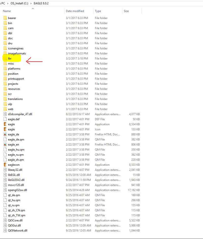
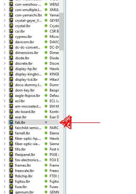
Eagle is a very user friendly software and you can find a lot of tutorials online. I also have downloaded the Fab library you can find it in the 'references' where you can find most of the components needed for the electronics exersices.
*NOTE*
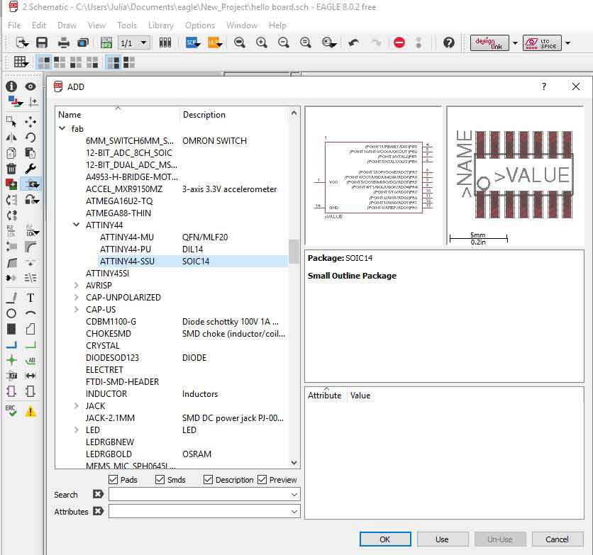
The first thing you should do in Eagle is to add your components, and you can check the fab library i have posted in the references for that. Make sure all libraries are highlighted with a green dot- otherwise they wont appear in the list of components. Always choose the "1206 components" as this is what you find in Digikey.
In Egale there are two basic viewports: the schematic and the PCB layout. I started by adding all the components to my schematic, and connecting them as shown in the reference. When everything seemed correct, I opened the PCB Layout only to find a mishmash of lines and components, which I had to put in place.
It was not a very easy process for me, and as i go deeper in the software i was figuring out stuff that made my life easier like Grid settings so I could have more accuracy with my lines (View/Grid/Size). And Layers tab to show and hide the elements.
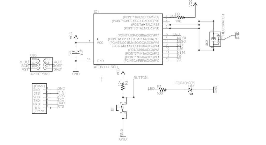
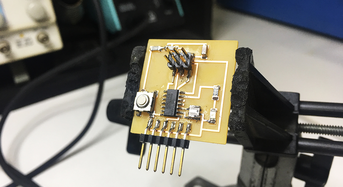
I learnt a lot from the process of redesigning the board and incorporating the button and LED. There are many rules concerning the minimum path dimensions, the clearances and the distance between the lines and the components which have to be respected in order for the board to work. Also, in order to add the LED and the button, I had to learn about the atTiny, its pins, what they do and how they should be connected with components.
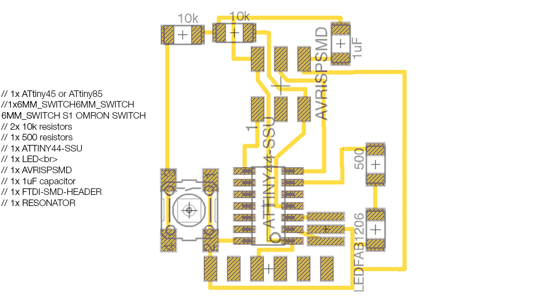
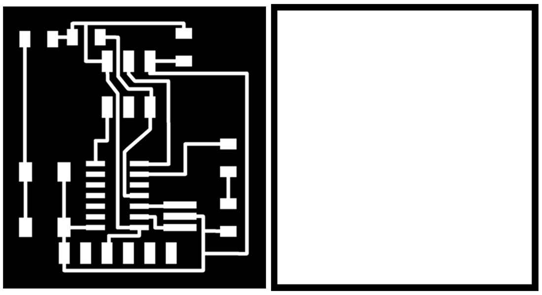
After having connected all the elements, I arranged them on the PCB board. Once this was finally done, I checked the design rules or DRC. This will make sure that the traces are separated enough for the machine to trace them. I set up the DRC with a wire-to-wire and wire-to-pad clearance of 16 mil and a minimum trace width of 16 mil, which is easily achievable using the pcb milling machines that we have.
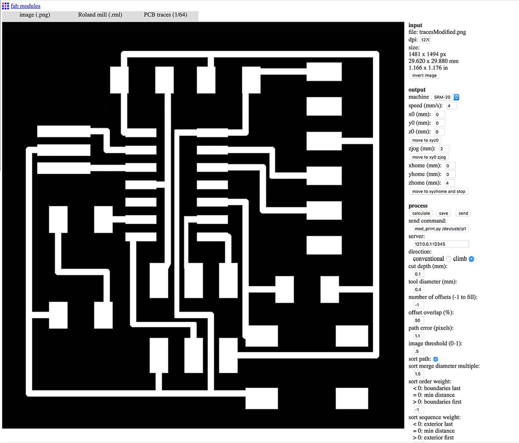
Then I Prepared the board for extracting the g-code on fab modules. First, I turned off all the layer but the top layer (traces only), which is the one I had my traces on. Then I exported the png by going to FILE, EXPORT, IMAGE. The settings have to be MONOCHROME and 500 DPI. I also exported the Dimension layer for milling the outside of the board. Once I had the png, I opened them on photoshop. It is important that the traces are in white and the rest is in black. If this is not the case, you must invert the image. Mine was alright, so I didn't have to invert it. But to make sure that the outline milling is not cutting any of our traces, is important to increase the image 1mm, which is the size of the outline trace.