Week 6
Redraw the echo hello-world board,add (at least) a button and LED, check the design rules, and make it.
This week's circuit design most people choose free eagle, there are a lot of teaching on the web. But I chose to use the launch of the RS Component Software Design Spark PCB, trying to learn and use it to draw the circuit board. Registered members can use the line model source, most of the components are free to use the library, but also has an analog circuit board 3D style, after the completion of the circuit elements can be directly exported table, provided the manufacturer of production preparation. Before drawing a circuit diagram, first refer to this website for SMD number and size relationships and package types.
本周的電路設計多數人選用免費的eagle,網路也有非常多教學。但我選擇使用RS Component所推出的軟體Design Spark PCB,嘗試學習及使用它畫出電路板。註冊會員即可使用線上的model source,多數元件library都可免費使用,也具有模擬出電路板3D的樣式,完成後可以直接匯出電路元件表,提供生產商備料生產。畫電路圖前,先參考此網站,了解SMD編號與尺寸關係以及封裝型式。
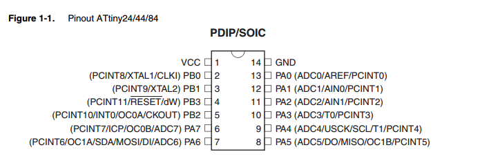
Reference Attiny 44 datasheet, which is a AVR microcontroller pin function as follows:
參考Attiny 44 datasheet ,其為一AVR 的微控制器,接腳功能如下:
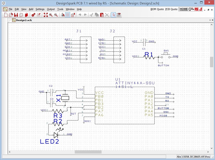
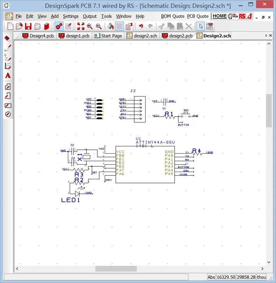
Designspark to redraw the figure below.
以Design Spark重新繪製下圖。增加按鈕及LED。
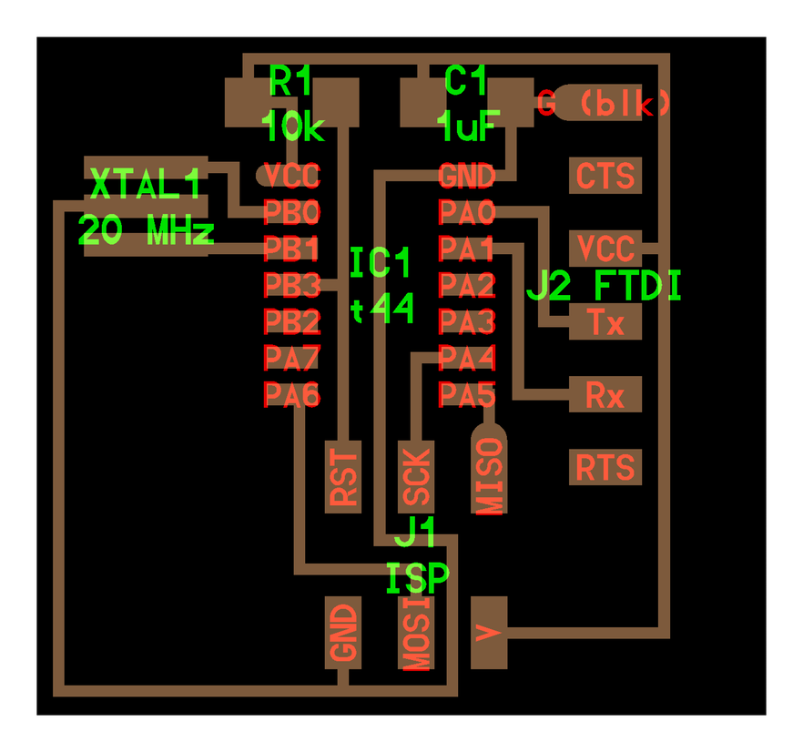
Seen from the datasheet, attiny44 8Mhz with internal oscillator, (Internal 8 MHz Oscillator) may also be used PB0 and PB1 pin external oscillator, I do not have oscillator Neto three feet on the feet so the use of passive bit 20Mhz oscillator, with 22pf capacitor become equivalent oscillator. LED connected to PA7, and the use of current limiting resistor. Button end of the ground (Gnd), at the other end of 10K resistor and PA3, the aforementioned other end of 10K resistor is connected to the power source terminal (Vcc). Schematic is as follows:
由datasheet可知,attiny44具有內部8Mhz震盪器,( Internal 8 MHz Oscillator)但也可使用PB0與PB1接腳外接震盪器,我沒有上圖內三隻腳的震盪器,所以使用20Mhz無源兩腳位震盪器,搭配22pf電容,成為等效震盪器。LED接在PA7,並使用限流電阻。按鈕一端接地(Gnd),另一端接於10K電阻與PA3,前述10K電阻另一端則接上電源端(Vcc)。原理圖如下:
Layout PCB
轉成PCB電路板:
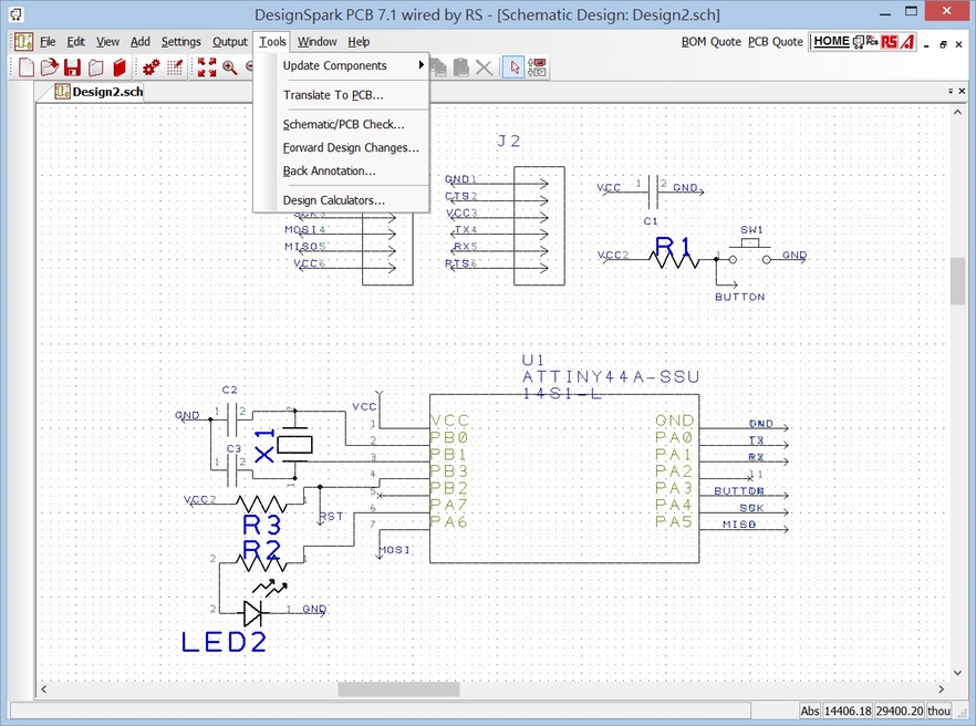
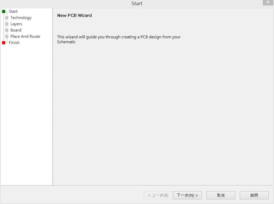
Select "Transtate To PCB"
Click"Next"
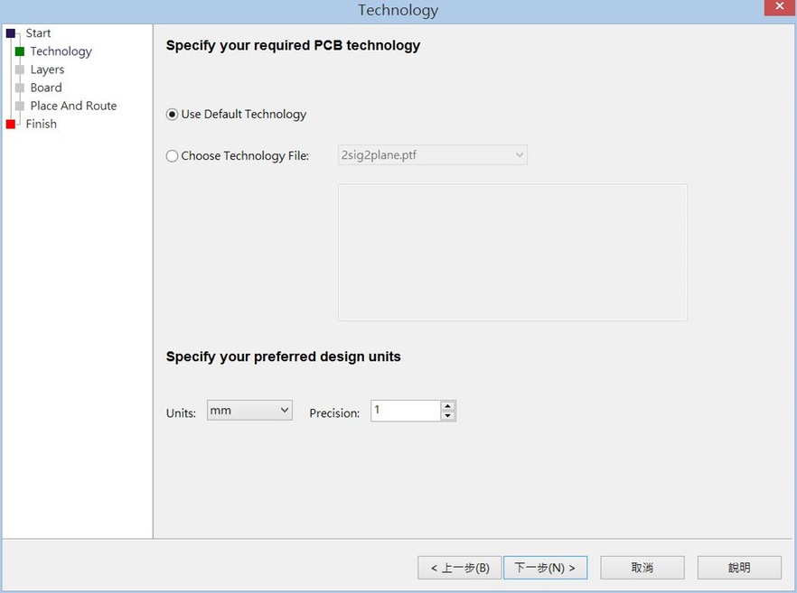
Select units. I select millimeter.
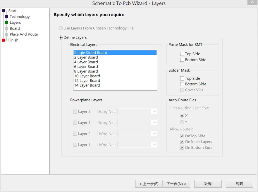
Select "Single Sided board" on demand select layers, we use single Bakelite (FR1).
Select "Single Sided board". 依需求選擇層數,我們使用單層電木板(FR1)
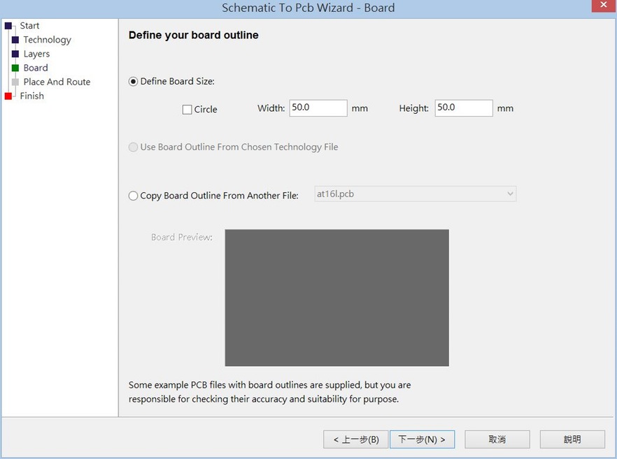
Set the board size
設定電路板尺寸
Click "Next" to place the outer layer of the first element, we manually placed by the.
Click"Next" 先將元件放置外層,由我們手動擺放
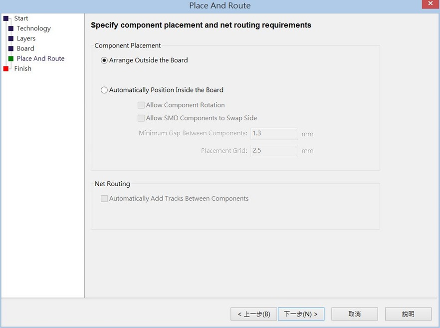
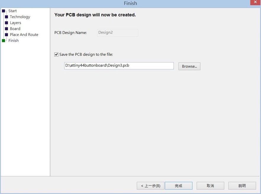
Click "Next" to choose a location
Click"Next" 選擇儲存位置
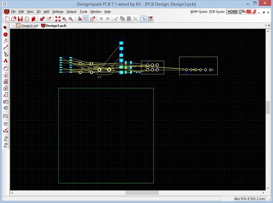
Click "Finish" will be in the following figure. The draw will be put to good element green box.
點選"完成"後會如下圖。拖動元件擺放至綠色框內
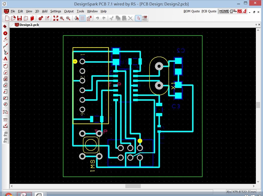
After the completion of placement, automatic routing using (Auto Route Nets) function, the software will automatically pull the line, if the part will not be automatically generated an error.
放置完成後,使用自動佈線(Auto Route Nets)功能,軟體會自動將線路拉出,若有無法自動生成部分也會提示錯誤。
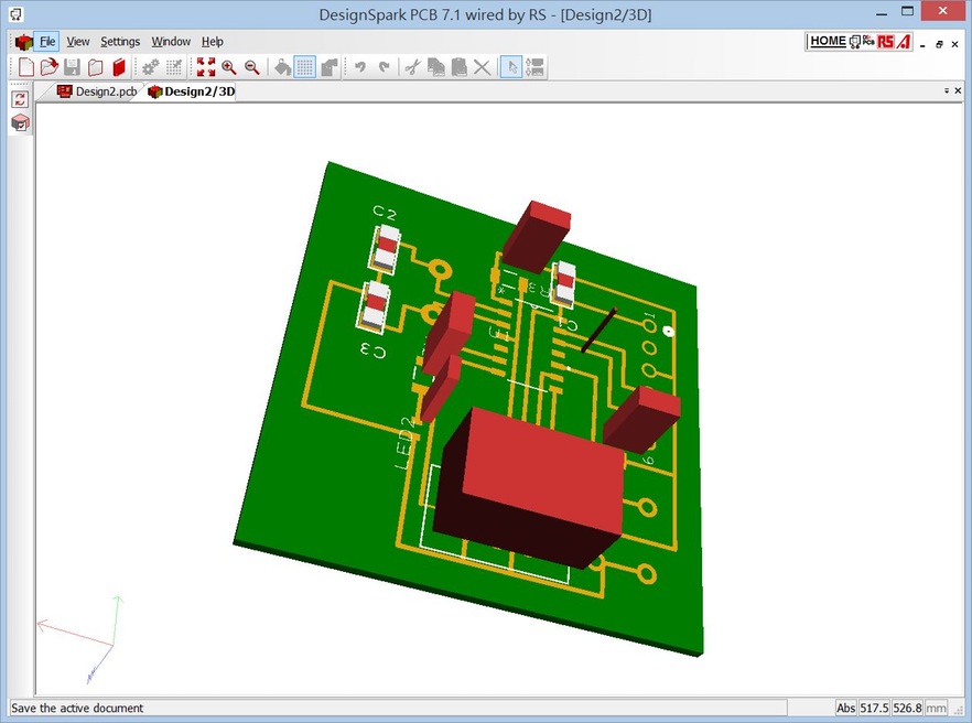
3D View, part of the element is not found SMD package, use the insert plate element.
3D View,部分元件未找到SMD封裝形式,使用了長度距離差不多的插板式元件
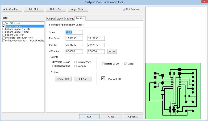
The PCB copper line export, use the "Manufacturing Plots" function.
將PCB銅箔線路匯出,使用"Manufacturing Plots"功能。
Just check the "Bottom Copper", as some element of plate inserted, check the "Mirror", the element can be both on the same side. Provided that all required vertical layout element has a polarity, otherwise the sign will mirror opposite.
只勾選"Bottom Copper",因部分原件為插板式,勾選"Mirror"後,元件才能都同一側。前提是具有極性元件皆須垂直布局,否則鏡射後正負會相反。
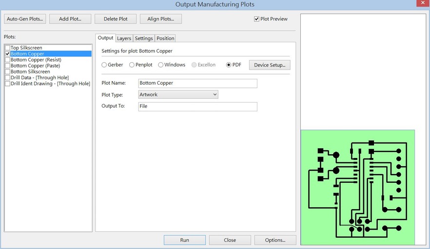
Select "PDF" after clicking "RUN".
選擇"PDF"後,點選"RUN"
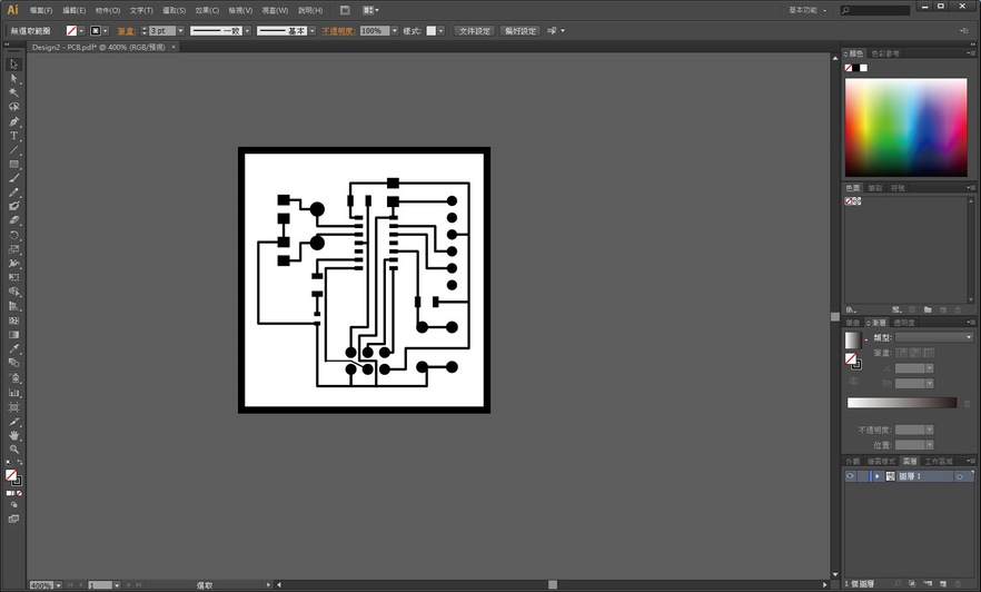
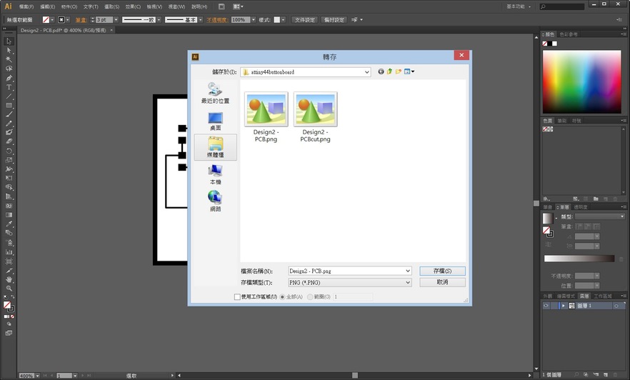
PDF format to be converted into * .png format, you can import Fab moulde turn into Roland CNC used * .rml format.
PDF格式需轉換成*.png格式,才能匯入Fab moulde轉成Roland CNC 所使用的*.rml格式。
In Adobe Illustrator open the converted PDF file.
以Adobe Illustrator開啟轉換後的PDF檔案
Plus the frame are cutting frame.
加上外框為切割框架
Move Drawing Format png, to the highest resolution (300dpi).
轉存圖檔格格式png,解析度調到最高(300dpi)
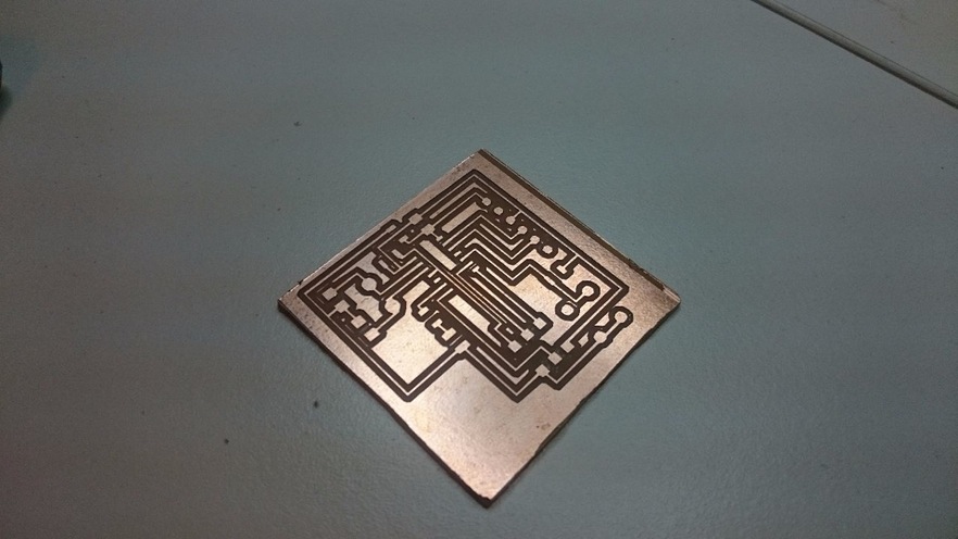
Fab module after use with SRM-20 cleavage products. But I found the bottom left of the line were too thin, broken line after the engraving can not be turned on.
參考week4,使用Fab moulde與SRM-20切割後成品。但發現左下角線路因太細,雕刻後線路破損無法導通。
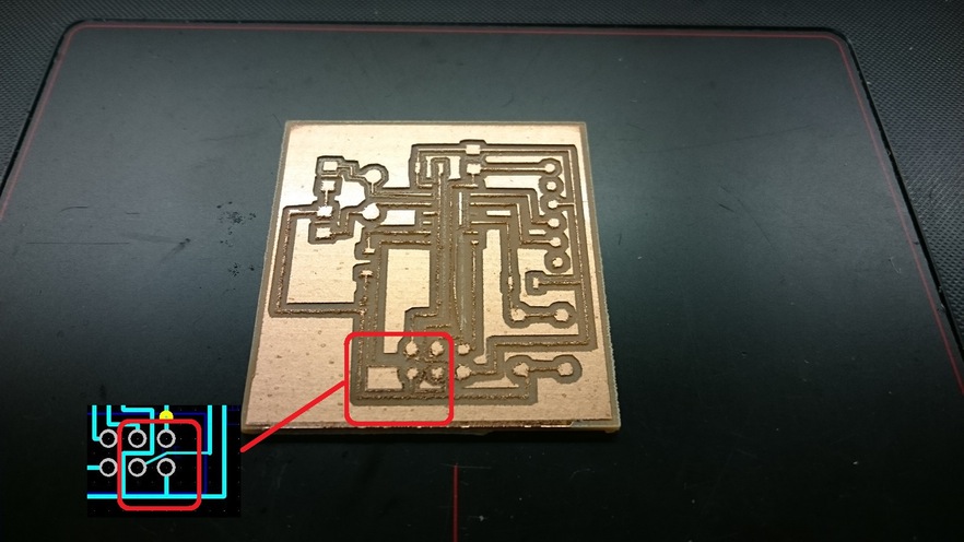
After research and try a variety of ways to modify the diagram, the IC power supply terminal coupled 0R (R4) resistance when using jumpers. 'This is the only method to avoid overlapping lines and lines too small problem.
研究及嘗試多種方式後修改了原理圖,在IC電源端加上0R(R4)電阻,當跳線使用。ˊ只有此方法才能避免線路交疊以及線路過細問題。
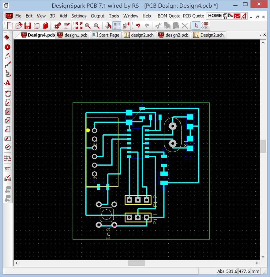
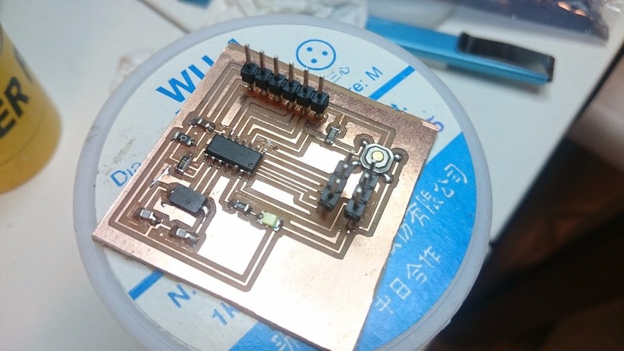
Re-Layout.
重新layout。並製作出電路板。
Attiny 44 IC element and welding.
焊接上attiny 44 IC與元件
Troubleshooting:
Design Spark PCB small preset component library, to be made after searching the web for download, but can not find many available sizes. Just pick similar elements or other package format close do use.
Design Spark PCB 預設元件library不多,都要由網路搜尋後下載使用,但許多找不到可用的尺寸。只挑選相近的元件或其他封裝格式接近的做使用。
I have yet to find Designspark PCB can export drawing (png) function can only be re-exported from the PDF graphics software (Adobe Illustrator) to dump * .png.
Design Spark PCB我尚未找到可以直接匯出圖檔(png)的功能,只能先匯出PDF再由繪圖軟體(Adobe Illustrator)轉存成*.png。
When the first edition Layout, poor line arrangement. Too close to the other elements that must be reduced diameter, carving fail. After several attempts, the IC power supply on the terminating resistor 0R When jumper (jump), so that Vcc smoothly around the outside, received ICSP.
第一版Layout時,線段安排不佳。過於接近其他元件而必須縮小線徑,使雕刻失敗。多次嘗試後,在IC電源供應端接上0R電阻當跳線(jump),讓Vcc能順利繞到外部,接到ICSP。
Tools:
Design Spark PCB
Fab Moulde
Roland SRM-20
Soldering toolkit
File:
attiny44buttonboard.sch
attiny44buttonboard.sch
File:
PCB footprint references
Book:3D繪圖與電路板設計:DesignSpark系列軟體指南
