Week 2
Model (raster, vector, 2D, 3D, render, animate, simulate, ...) a possible final project, and post it on your class page
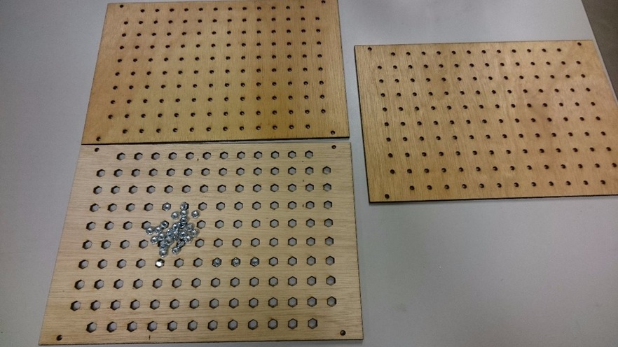
Before made the USBISP Writer, I found that CNC machine's cutlery can't flat on the plate when I making the circuit board, so I use the double-sided tape and board, its can help machine to increased and fixed the circuit board, but the problem is I have to clean the board every time, and the board is uneven of the Carving face.So I change my mind, start to make a Fixture of the circuit board.To make the Fixture, it will making by 3 boards with some screw nuts in the middle, and there has some screws' hole I can according to size of circuit board fixed with screws.The boards produced by Laser cutting machine.
在第四周製作USBISP燒錄器後,發現SRM-20製作電路板時,刀子移動降到最低時距離底板上有一段距離(刀具無法加工平貼於底板的電路板),所以使用雙面膠及木塊升高且固定電路板,但容易造成雕刻面不均勻,且容易殘留髒污及殘膠,不易使用。因此以Inkscape繪圖製作電路板夾具。以三層木板組合而成,中間層設計可以放入螺母,再由兩片木版夾合,上面的孔洞對應螺母,依雕刻電路版大小挑選孔洞,將螺絲及墊片鎖上可固定之,且四周留著可以固定於SRM-20底板的螺絲孔,木板加工皆由雷射切割機完成。
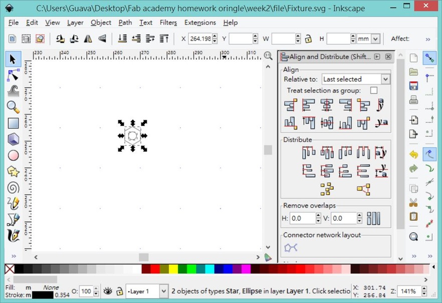
In the Inkscape, I can use shape tools to help me graphing, it's include Roundness, Rectangle and Hexagonal. And using the Align and distribute function to align objects.
所有形狀皆由左側功能列完成,包含圓形、矩形、六角形。使用Align and distribute功能進行對齊物件。
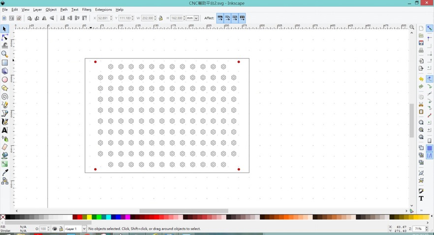
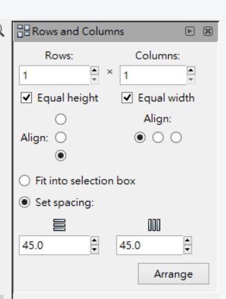
Using Rows and Columns function to generate a matrix, and editing the relative distance.
使用行與列進行排列出矩陣型態,並可調整相對距離。
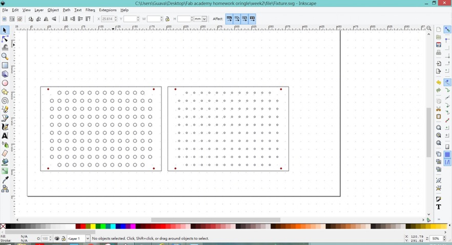
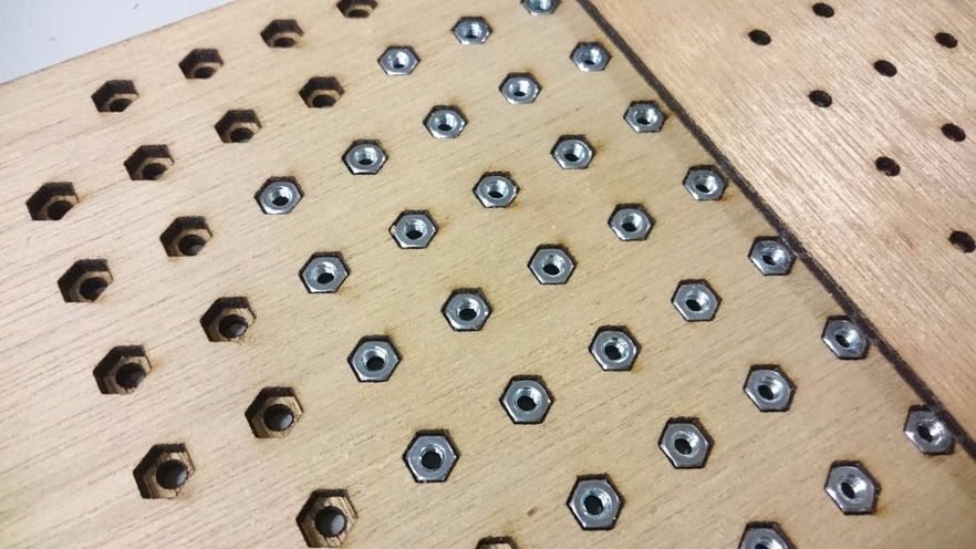
Copy the completed one and delete some objects that I don't need.So you can see as shown below, the left one has bigger hole that's the screw nuts hole; right one is the upper and lower board that can caught middle board with screw nuts in it.
最終完成圖再複製,刪除不要的圖形,左圖為中間板可放置螺母;右側為上、下板,夾合螺母。
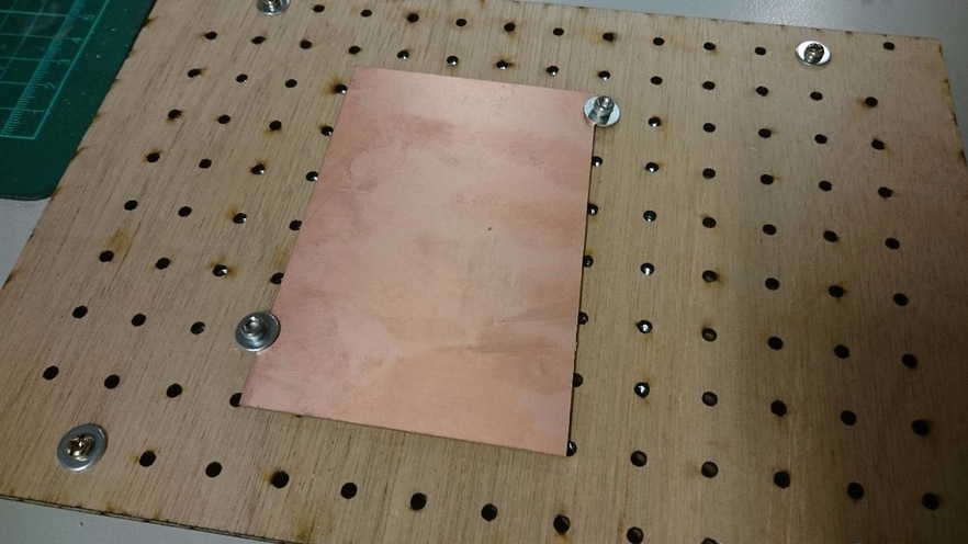
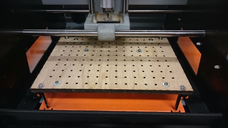
So here's the actual one.
實體物品圖。
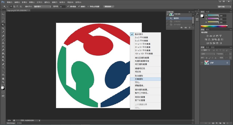
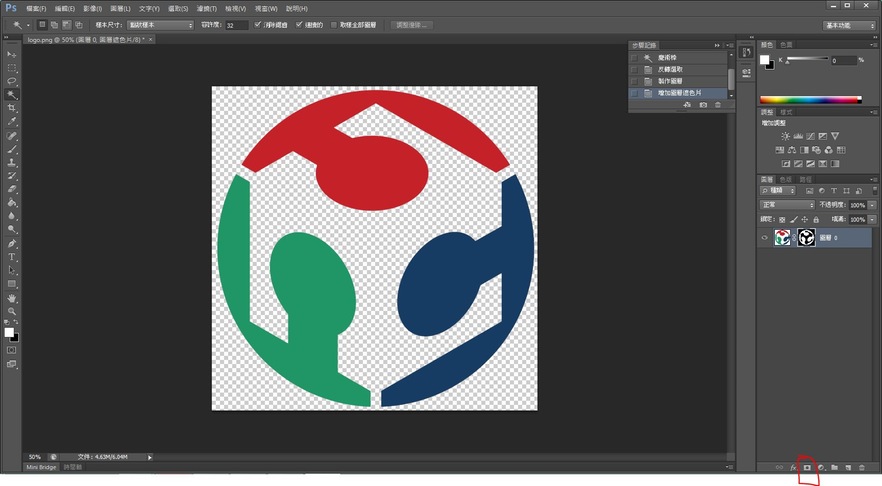
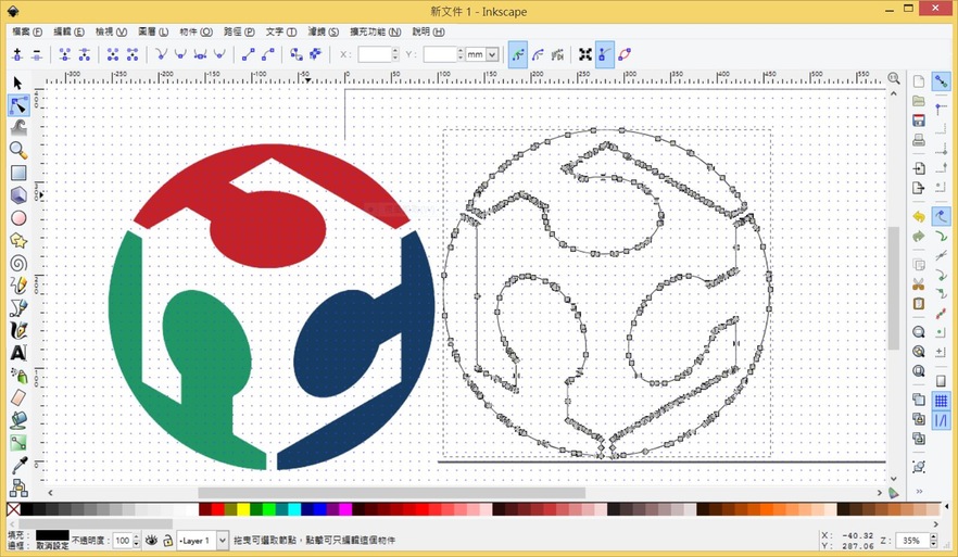
And I try to change Fablab's logo from bitmap to vector by Photoshop and Inkscape, so I can use the Laser cutting machine to process my homework.First, use Photoshop to open the Fablab picture, and use the Magic wand tool to select picture's edge, than delete white area turn to PNG format. This image has become my home page icon. It will cover the basemap, if I use the image which is the jpg format.
本周我嘗試使使用Photoshop與Inkscape將Fablab Logo由點陣圖片形式轉換成向量圖檔,此檔案將可使用雷射切割機進行切割或雕刻。圖片由Photoshop開啟,並選擇魔術棒做邊緣的判斷,將白色區域做圈選後反轉選取要留下的部分,再製作成遮色片,可以去除背景轉存成透明背景色的png格式。此圖片成為我網頁中首頁的圖示,若使用jpg圖片,將遮蓋後面底圖。
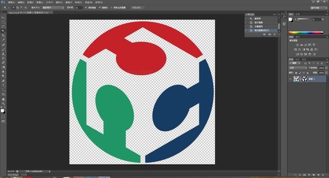
Second, open the new file in the Inkscape, and I have to ues color as a basis because the color of Fablab's logo, that has significant difference in the Trace Bitmap function.
再由Inkscape開啟新檔,使用描繪點陣圖(Trace Bitmap)功能,因Logo具有明顯顏色差異,因此以顏色(Colors)作為判斷轉換依據。
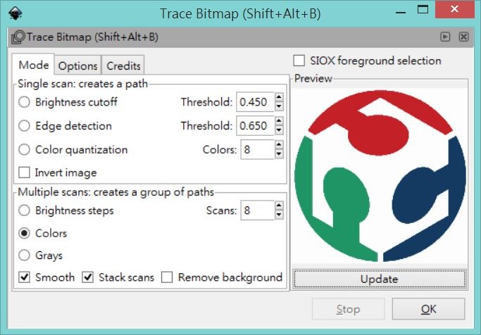
Here's the completed example.
完成圖如下。
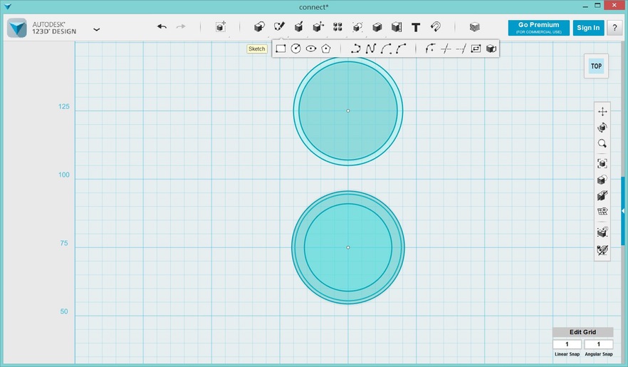
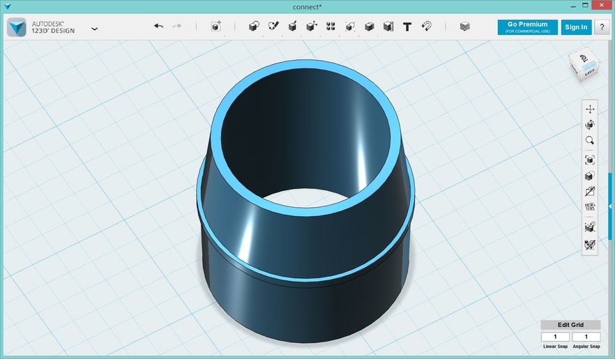
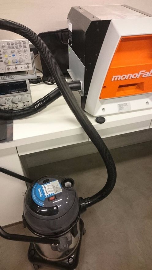
Now, I'm thinking about 3D model, so I start to use the 123D Design, a free online 3D modeling software, I will use this modeling software to make a Roland SRM-20 connector with the vacuum cleaner machine.First, use the Geometry Tools to draw a shape on the sketch plane, that already measured size of the sketch plane.
3D圖形我練習使用123D Design,因為其容易取得及使用且免費,此次所做的物件是Roland SRM-20與吸塵器管路的連接器。所有圖形皆由平面草圖(Sketch)開始,量測好所需物件尺寸,先在圖面上畫出投影面的形狀。
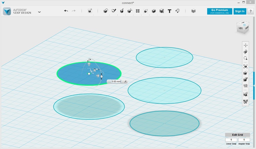
And Stretch and whirl to shape 3D model from the Constructor function.
再由構造(construct)特徵功能進行拉伸、旋轉等製作出立體結構。
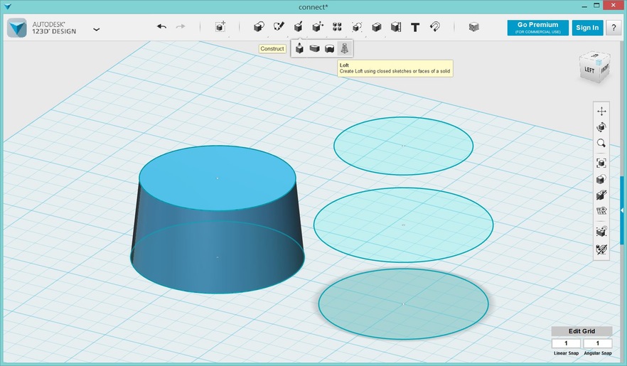
I still can bonding, subjoin and lessen each part of the model until I finish the work.
結構同樣可進行黏合、增加及修剪,直到完成作品。
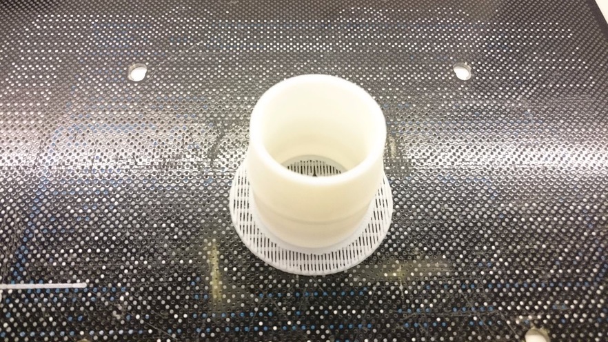
So this is the example from printing by 3D printer. I'm using the UP! Box machine, this machine can be used ABS and PLA wire. Between the two materials differences can reference from wiki link. Both they are polymer materials, but different melting points and physical properties. ABS has high strength, commonly used in the life of a variety of plastic products, but PLA is more environmentally-friendly.
使用3D列印出成品:我使用的是UP!Box機台,此機台可以使用ABS與PLA線材。兩者的差異可參考維基連結。都是高分子材料,但熔點及物理性質不同。ABS強度較高,常用在生活上的多種塑膠製品,而PLA材質則對環境較為友善。
UP! Box operation simple, Print area of up to 255 × 205 × 205 mm (W × H × D). Closed housing allows a more uniform temperature more stable printing environment. Filtration systems filter the micro particles produced from printing.
UP!Box機台操作簡易,列印面積可達255 × 205 × 205 mm (W × H × D) 。封閉的外殼可以讓列印環境較為均溫更為穩定。過濾系統則讓列印中所產生的微粒子不易散發出。
Operation steps:
操作基本步驟
Initialization
機台初始化
Loading 3D file(*.stl)
載入3D圖檔
Adjust the print direction of object
調整物件列印方向
Require preheating plate, when use ABS materials. It can avoid corners warping.
若使用ABS線材需要進行底板預熱,避免邊角的翹曲。
Choose Print Parameters
選擇列印參數
Printting
進行列印
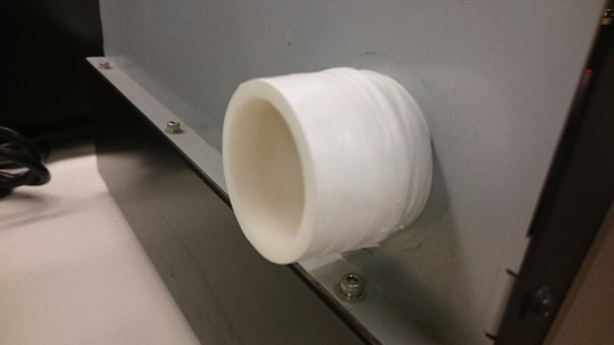
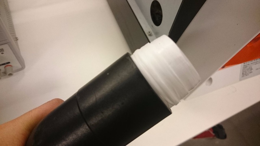
Connect this two machine by Teflon tape, its can help the Bridge no leak air.
纏上鐵氟龍膠帶防止漏氣,連接上兩個設備。
Troubleshooting:
Elimination of size and machine making errors. And the Fixture of the circuit board, I have To duplicate many times to have a worthy of use one that tally the size of SRM-20's holes.
消除量測及設備製作誤差。電路板切割夾具經多次製作、重繪,才符合SRM-20底板孔洞尺寸。
Tools:
Photoshop
Inkscape
123D Design
Laster Cut
3D Printer
File:
Logo
Connect
Fixture
