Assignment 4: Electronics Production
PCB fabrication
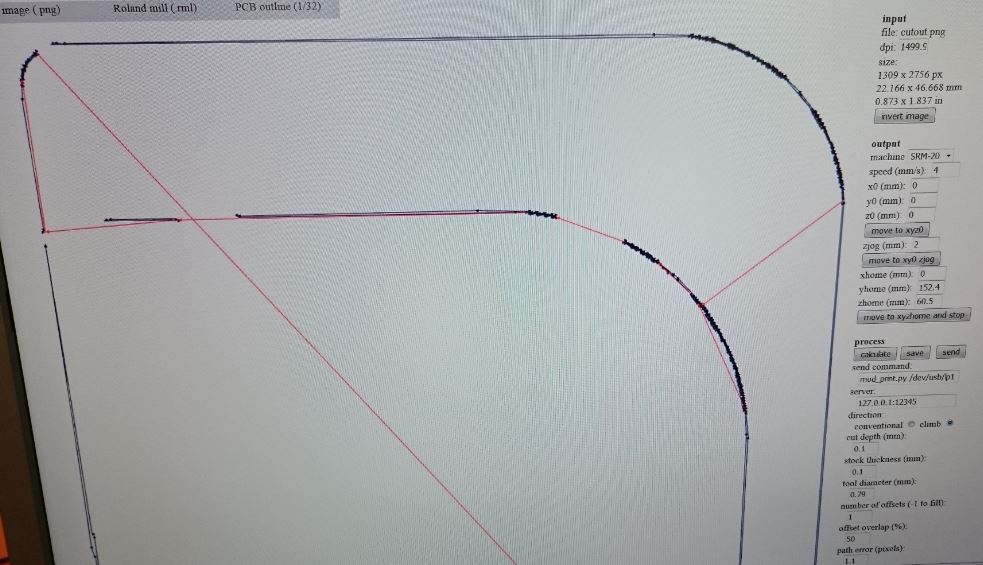
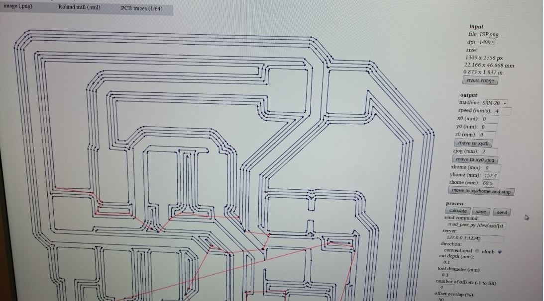
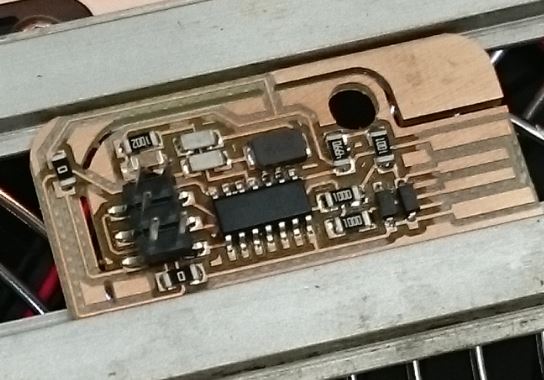
We decided to fabricate Valentin's
version of the ISP-board. At first I tested whether the cutout
of 0.1 mm is enough. The board billet was slightly curved in the
corner where the SRM20 origin was set, as seen in the picture below.
As a result the cut was not through the copper, so 0.2 mm cut
depth was used for the first board.
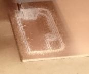
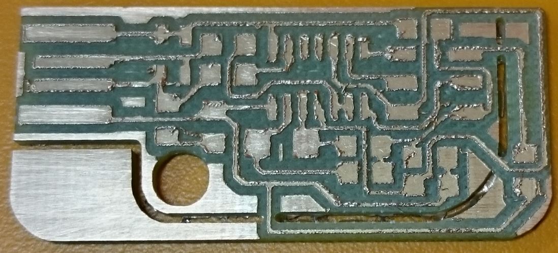
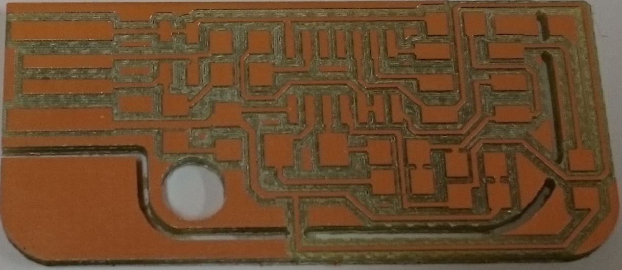
Actually, the first board didn't come out that well. Against Neil's
recommendation, we used FR4. The result is presented in the
following picture, in which the pcb was photographed after polishing
with steel wool. It was even worse before. The reason could be
a worn drill bit, but that needs to be tested.
So, we changed the tool to a v-shaped one with a width of 0.2-0.5
mm, that looks exactly like this.
I changed the tool diameter to 0.3 mm in fabmodules. Now the milling
result was perfect to my eyes. Only the copper island beside the USB
data signals had to be removed with a knife. Later I was told by
Juha-Pekka Mäkelä, that there is a handy calculator
to determine the v-shaped tool cutting width depending on the
cutting depth. In this case 0.4 mm tool diameter would have been
better.
Assembly
I have about 40 years of experience in hand soldering, so I decided
to do the assembly with a proper surface mount component prototype
assembly line that we have in our Fab Lab, because I had to refresh
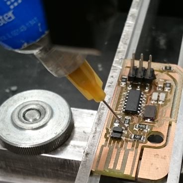
my skills in using those tools. I used the solder paste dispenser of
the Essemtec SMT assembly system to put soldering paste to the pads.
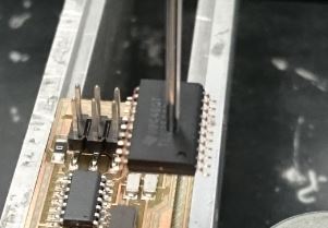
Then I placed the components with the pick and place system with a
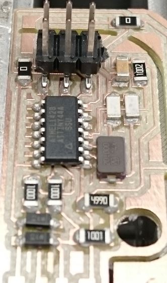
vacuum nozzle. The picture in the middle is the board ready to be
soldered using a reflow oven. The left picture shows the paste
dispenser, whereas the picture on the right has a non-related
component held by the vacuum pick and place nozzle..
Soldering
After the warm-up period
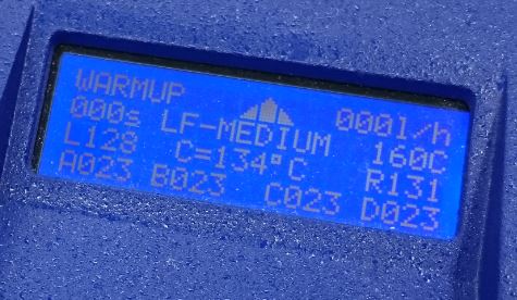
the board was placed in to the holder.
The oven then preheats the board
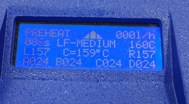
and reflows it.
As the result, we have a freshly baked pcb.
Programming
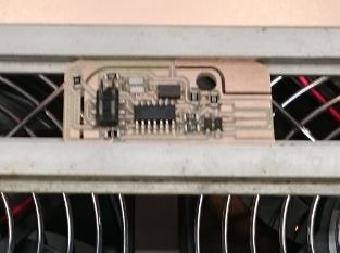
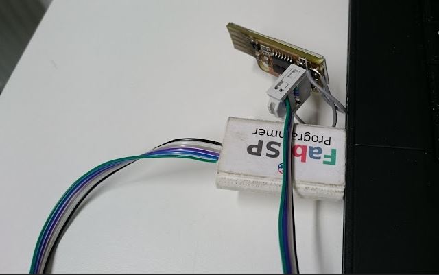
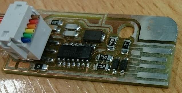
I had earlier programmed my usbtiny programmer with Juha-Pekka
and Dorina, without properly documenting the process myself. So
I went through everything again to my already programmed
usbtiny, to which I had to add the jumpers, which were remove
after initial programming.
The following resources were used:
FAB ISP programmer provided by Jani
Fabacademy.org tutorial
for FabISP Programming.
Install software tools:
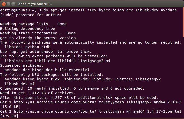
Open Terminal and type:
sudo apt-get install flex byacc bison gcc libusb-dev
avrdude
Then type:
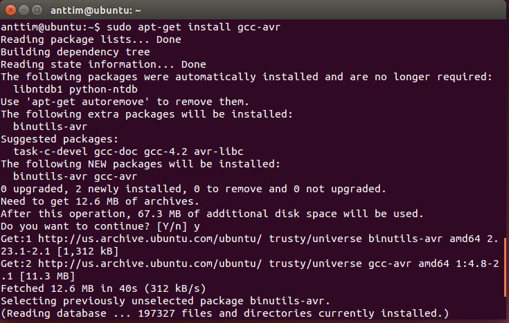
sudo apt-get install gcc-avr
- type "y" when asked to do so by your system
Then type:
sudo apt-get install avr-libc
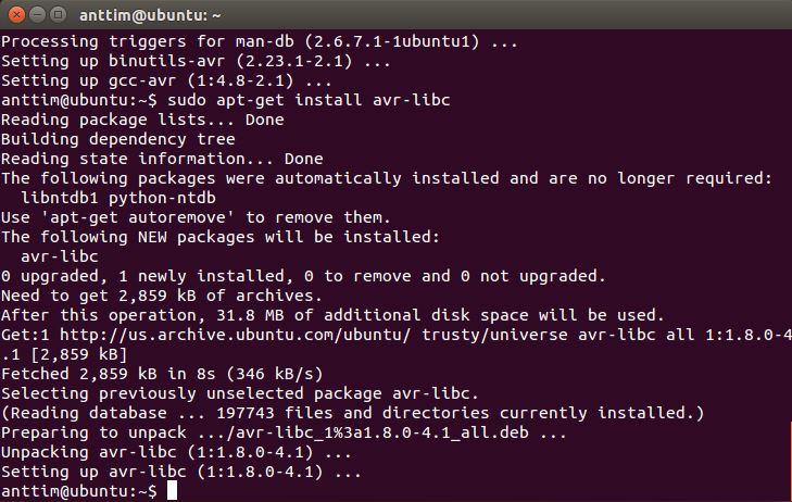
Then type (may already be installed):
sudo apt-get install libc6-dev
And it was already installed.
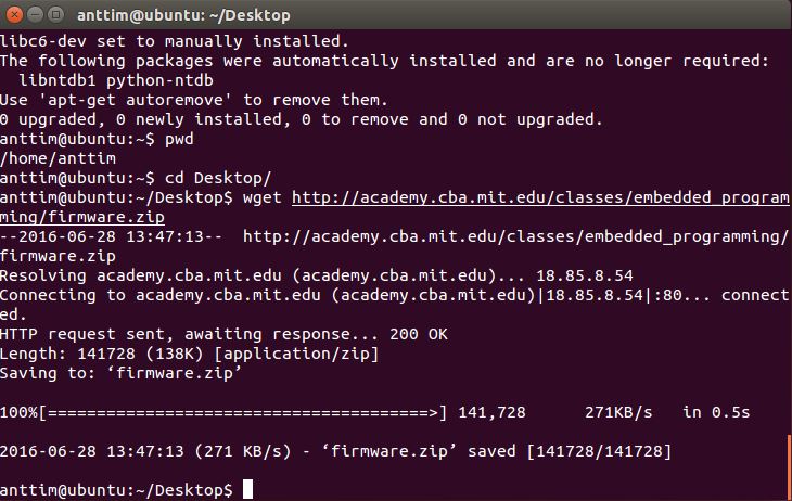
Download and compile firmware:
Download and Unzip the Firmware:
Move to the desktop
cd
~/Desktop
Download the firmware from the Fab Academy Electronics
Production page.
wget
http://academy.cba.mit.edu/classes/embedded_programming/firmware.zip
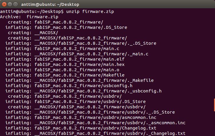
Unzip the firmware
unzip firmware.zip
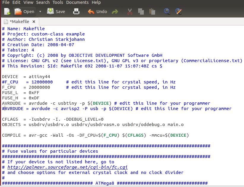
Edit Makefile:
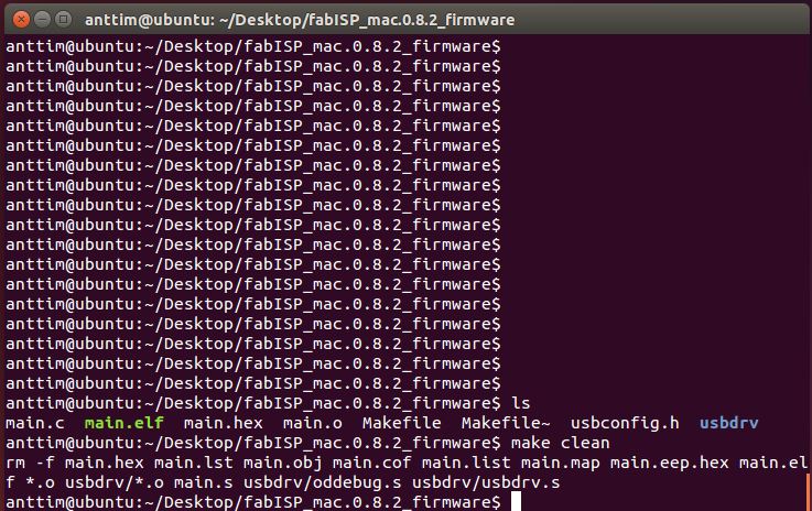
make clean:
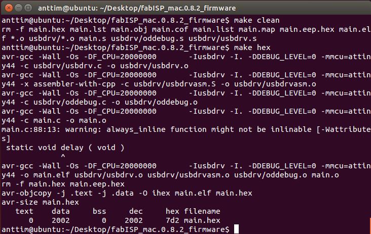
make hex:
make fuse:
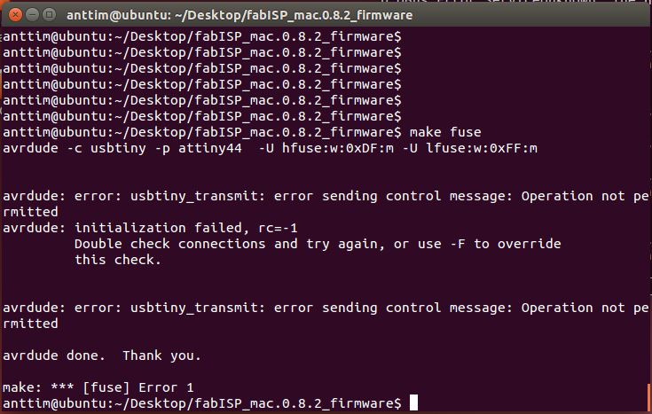
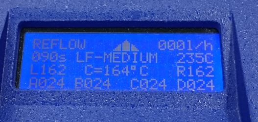
Make fuse gave me an error, as shown above. Googling the error
lead me to an instruction
suggesting, that I have to create a 10-usbtinyisp.rules file in
directory /etc/udev/rules.d with the content:
SUBSYSTEM=="usb", SYSFS{idVendor}=="1781",
SYSFS{idProduct}=="0c9f", GROUP="adm", MODE="0666"
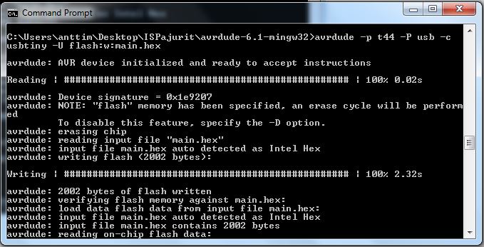
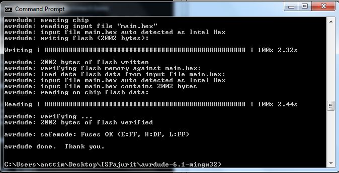
That I did, but it didn't help. However, I now had the main.hex
file, which I programmed in Windows with avrdude:
Update:
I remembered, that the faculty workshop uses chemical tin to
coat the copper with a thin layer of tin. So, that is what I did
to the USB-connector.
http://www.bungard.de/index.php/en/products/surfaces/bungard-sur-tin
Home