Week 06
This week was all about electronics design. Our goal was to draw the schematics and prepare a board layout to mill it and solder all its components. We mainly used a software called Eagle (Easily Applicable Graphical Layout Editor), which is a flexible and expandable EDA schematic capture, PCB layout, autorouter and CAM program.
This was my first time doing this so I was a little bit worried. At the beginning I was lost, I never heard about most of the technical terms, but after a while, I started to understand the logic behind the design.
It was an interesting week, hard work and lots of learning.
Objectives
Redraw the design of the echo hello-world board
Check the design rules
Use at least a LED and a BUTTON
Weekly Progress >
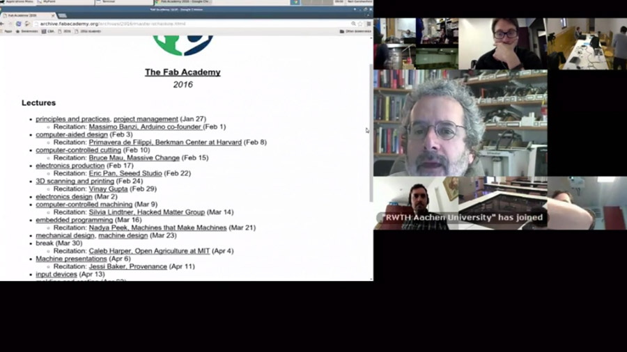
First, we had our weekly lecture with Neil Gershenfeld, you can watch it here.
Kenny Cheung gave this week’s lecture, he talked about How to make almost anything in space.
How to make almost anything in space.
Assingment >
Before beginning we had to take a look at this tutorial about designing our hello board with eagle. Also to get more familiarized with what was going to happen during the week, we watched other tutorials. You can watch them here: 1 - 2
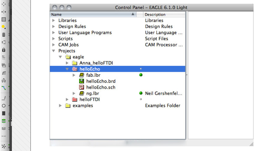
For designing we used Eagle, you can find it here.
We also used the fablab component library, find it here.
First steps was to get familiar with the board layout. Ferdi, our tutor, explained to us the basics of eagle and how to use it. He did an example which we followed; he explain each part of the board, how it works and how to draw it.
Two key words: Schematics and Board Layout.
Schematics: in electronics is a drawing representing a circuit. It uses symbols to represent real-world electronic components. The most basic symbol is a simple conductor (traces), shown simply as a line. If wires connect in a diagram, they are shown with a dot at the intersection.
Board Layout: The board layout shows how the electrical components and traces will be laid out on the board.
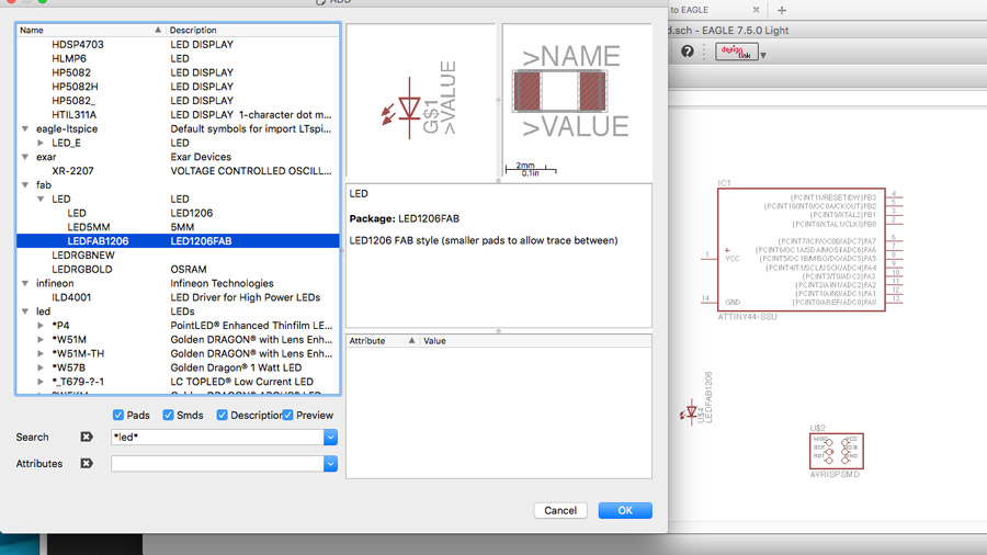
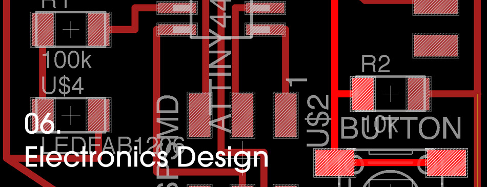
The third and the most important part of electronic design is the components. To build this hello board we used the Fab Eagle Library.
This is the list of components I used.
ATTINY44-SSU x 1
LEDFAB1206 x 1
CAP-US1206FAB x 1
RES-US1206FAB / 100k x 1
RES-US1206FAB / 10K x 2
FTDI-SMD-HEADER / 1X06SMD x 1
6MM_SWITCH x 1
RESONATOR 20 M x 1
AVRISPSMD / 2X03SMD x 1
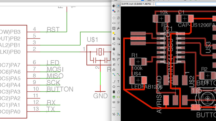
After having all components selected it was time to start with the schematics. Two things to keep in mind when using eagle is that the program produces two different files for the schematics (.sch) and the board layout (.brd), those files work together so any changes you make to the schematics get reflected on the board layout instantly, this is really helpful when you are checking/fixing your component connections.
Important considerations:
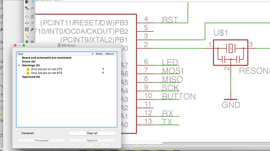
Use the Electrical Rule Check (ERC) to make sure your connections are correct.
Be sure your connections are really connected and avoid double lines; zoom in.
Be sure of that the value of your components is the same on your connections.
Do it slow and pay attention to what you are doing, this will save you time later.
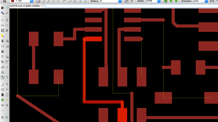
Next step, preparing the board layout. This part can be tricky because its easy to spend a lot of time trying to fix distances and misconnections, so as I mentioned before, you have to do it orderly and paciently.
Before beginning with it I positioned each element to make easy its connection, then I changed grid distance. I had troubles here because my distance was to much, every time I moved my lines got to close, so I had to change it several times.
At the end I used: Size: 0.0175, Alt: 0.00109375, Inches
* Traces should be 0.4064, because of the milling machine drill bit.
Another thing to know is that you have an error check option for the board layout, it is called Eagle Design Rules (EDR). Keep on working until you get no errors.
It took me some time to finish my design but I did it!
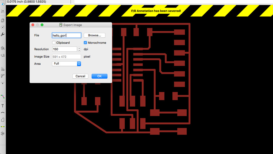
The next step is to export your layout to begin with the milling process.
Export to png @ 500dpi - monochrome
You can download the eagle files here.
You can download the PNG files here.
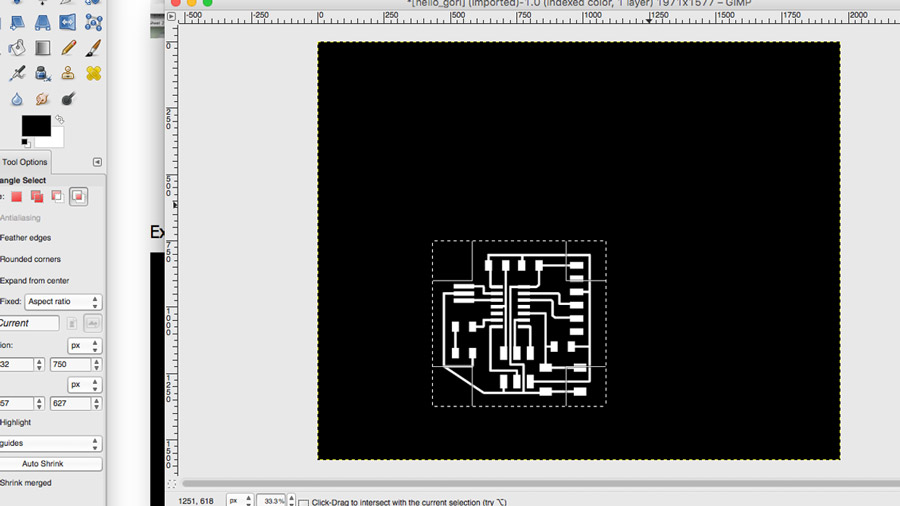
Then crop the png to the desired size. Remember to leave enough border space, that space can be useful to support some components. I left 3mm.
Before saving check:
Your image is in black/white color profile, this is important, If you are in the wrong settings your milling process could fail.
500 DPI
Check your document size.
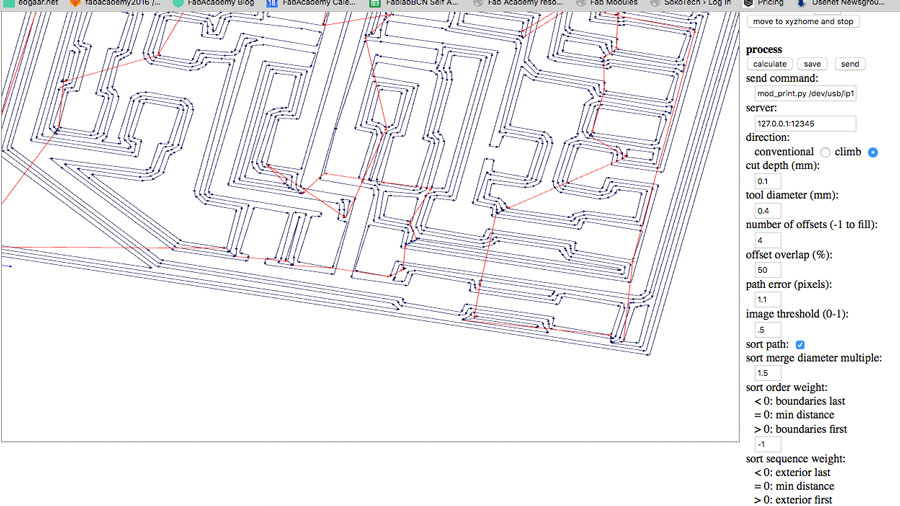
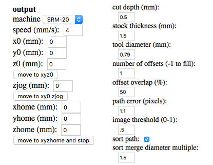
I used the SRM-20 for the milling process with this settings:
Traces
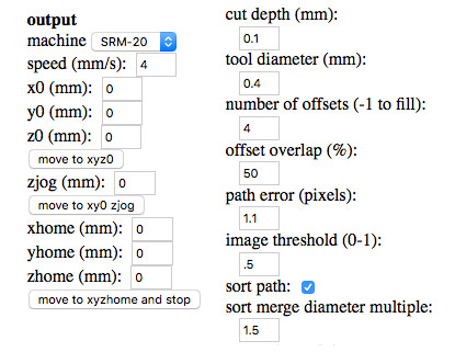
Outline
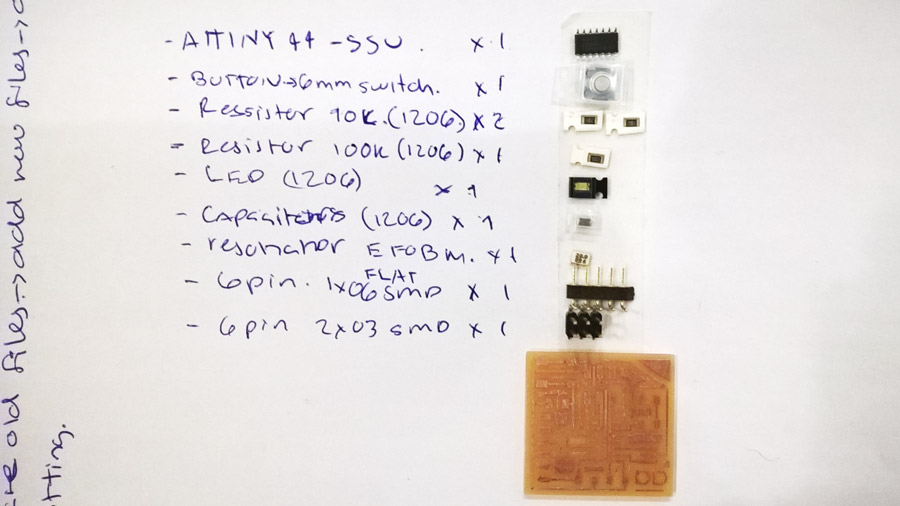
Before soldering; component list + board layout milled
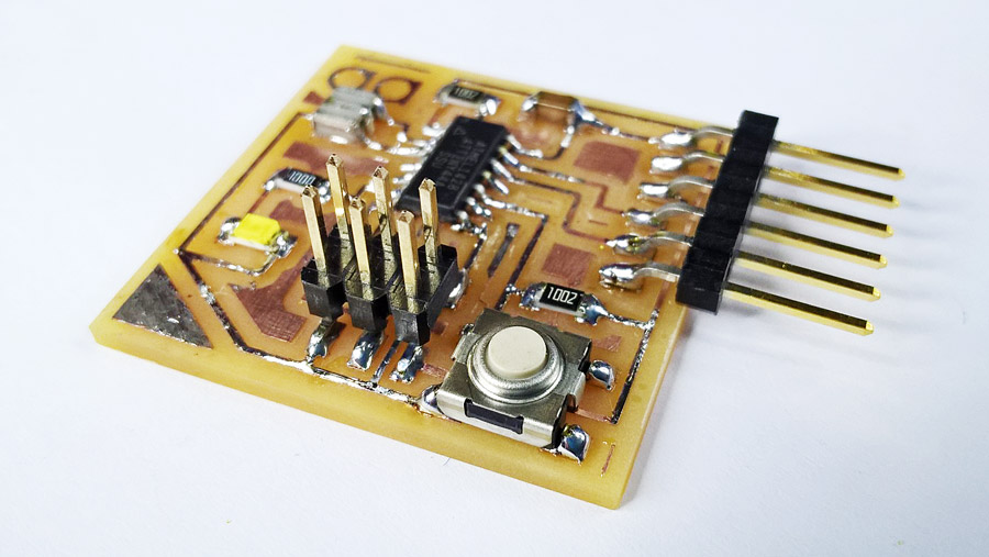
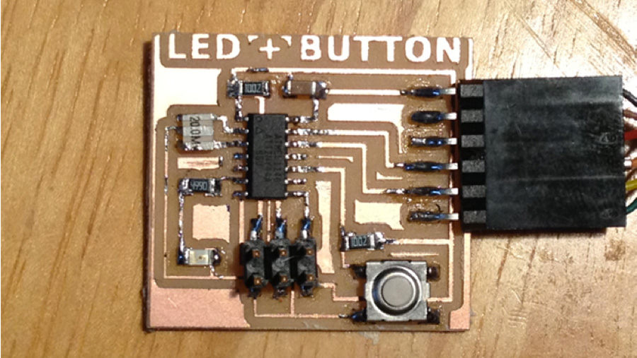
And this is the result, my first hello board! Am really proud to have done this, even though I still have a lot of questions on how electronics works, I feel great and eager to learn more.
I'll keep practicing on electronics design, my next exercise will be try to use all available pins to add another connector to be able to connect shields.
