Home
Biography
Projects
Final Project
Networking
This week I plan on using my boards from both Input Devices and Output Devices to communicate over an I2C connection (what they were designed to do). I plan on sending data from the master (an ATMega328) to two slaves (Two ATTint44s) which will switch LEDs on and off. I will be using this in my final project, with a different master board (a 32u4 and a 1284P) for more complicated things
Design
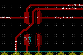
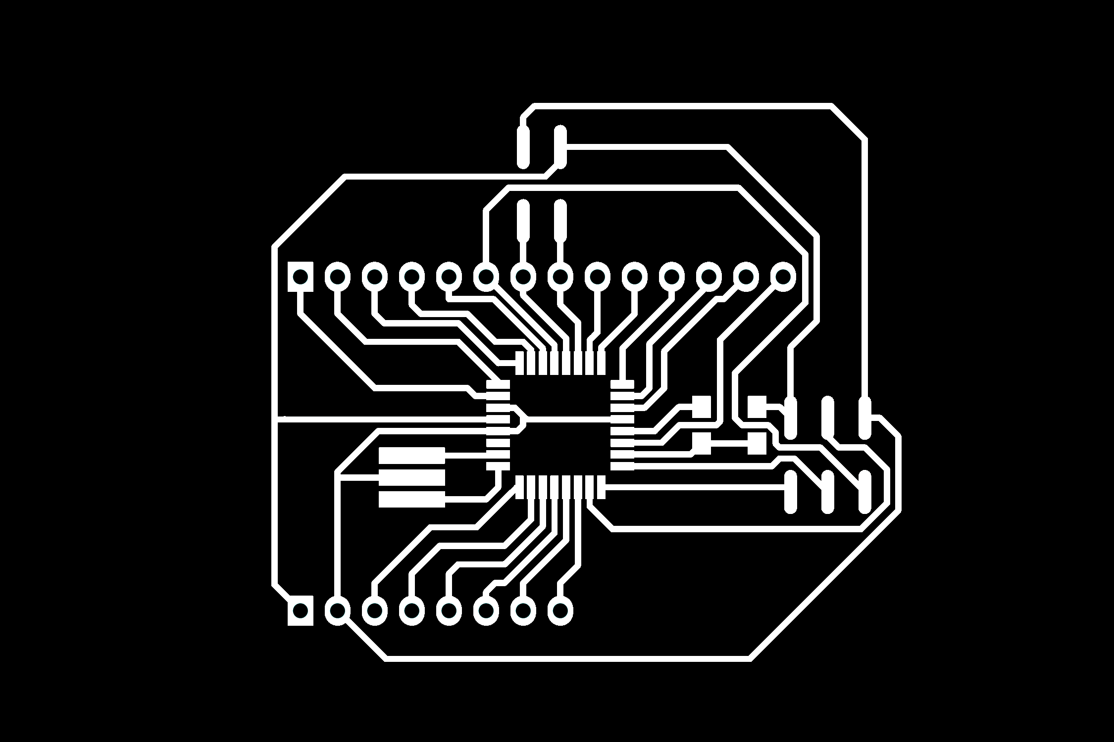
The boards I am using are no different than the ones I have used in Input Devices and Output Devices, with the exception of making necessary modifications to the master board. On the initial master board, I had the positive and negative pins on the I2C header switched, which could cause either the msster to explode (not really, but it does break) if powered from a slave or the slaves to explode if powered from the master. The switch was easy and actually reduced the number of components I needed, because the switch allowed me to remove a jumper. Below you can see the fixed header layout.
Thankfully, the SDA and SCL pins were in the same configuration, so no changes would be needed.
Production
The production process is the same Vinegar-Peroxide-Salt
mixture I have used in both, using the laser cutter to etch away masking tape to use as a resist. Since the boards were already made (with the exception of the new master board), I didn't need to etch any more boards. This is the list of the general steps I took to etch the new master board:
- Export the board to an SVG in KiCAD, and edit the SVG in GIMP witha resolution of at least 750 DPI
- Convert the images to black and white. Make the traces white and the backgroud black. Also make the through-hole holes black
- Export again to a PNG and import the file into AI. You could really go directly to AI, but this is the process I used.
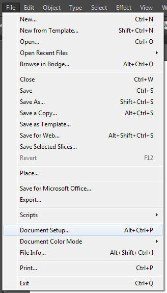
- Edit the artboard to the size of your blank PCB using File>Document Setup>Edit Artboards and modify the values at the top.
- Then arrange as many boards as possible on the artboard. Less exposed copper, less etch time. Make sure the background is black
- Now trace the image while the image is selected. This rounds the edges of the traces, reducing the chance that jagged edges will contact each other in the final product.

- Now apply masking tape to a blank PCB and squeegee out any air bubbles. Apply double sided tape to the backside of the board to prevent the board from sliding around inside the mschine.
- Send the file to the laser cutter. I used 50% speed and 50% power for our 40W Epilog, bud settings will vary based on laser cutter. Usually this takes two passes.
- After the second pass, remove the board and the double sided tape. There should be only a thin layer of adhesive left on the board.
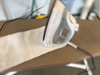
- Take the board to a clothes iron and turn the iron on. Place the board inside a cloth and press firmly with the iron for about 10 or so seconds. Do not rub or use steam, since this could remove the resist on the traces. Ironing the board reduces the chances of the resist lifting off in the solution. Image is blurry because I'm a bad photographer.
- Prepare the etching solution using a 1:1 ratio of vinegar and Hydrogen Peroxide. Add some salt to accelerate the etching, but make sure that the salt is the kind without anti-caking agent, as this could neutralize the vinegar.
- Wait, this proces takes awhile.
- Once the board looks done remove the board (wear gloves) and inspect the board for any copper left. if there is copper left, place the board back into the bath for a little while.
- Wash the board off. Now is a good time to remove the etching resist.
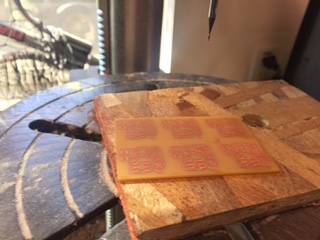
- Drill holes in the board where you need them using a drill press. Using a drill press ensures that the holes will be perpendicular to the board and accurate.
- Now solder the components to the board. it helps to sand of any oxidation and use solder flux. I find it easier to place lower lying components first and move to taller ones.
- You now have a complete board ready for programming.
Programming the Slave
Programming the slave for Networking turned out to be harder than I thought. I assumed that because all of the schematics I have made in KiCAD show SDA and SCL pins, the ATTiny44 had native I2C support. It does, in the sense that the 44 has a USI or Universal Serial Interface. This is what drives the SPI capabilities of the chip, and others have written libraries using the USI for I2C.
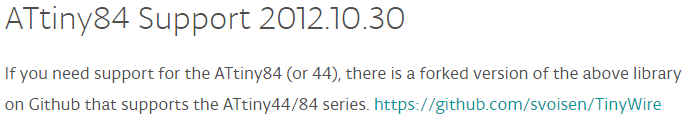
Unfortunately, I could ony find Arduino libraries for the ATTiny85, since this is found on several arduino boards. I could find master code for the 44, but no slaves. I finally found that an update on the TinyWireS GitHub granted I2C abilities to the Tiny44. The GitHub page can be found here.
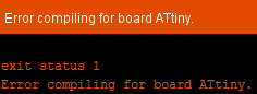
Actually using the library is difficult. You can'y just drop the library into the code and use it. There is a lot of stuff that needs to be done within the IDE to use it and compile correctly. This is what happens if yoy just use the library directly:
This is what you need to prevent this from happening, found in the exmple code included in the library:
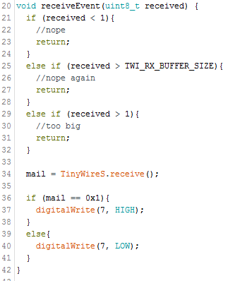
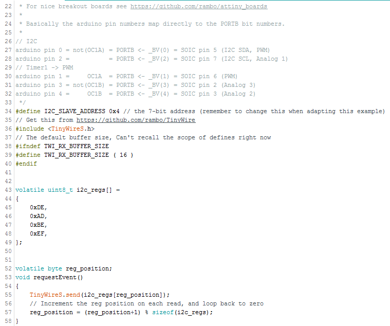 Frankly, I can't be bothered to write all of that from scratch, so I will be copying all the code from the example and cutting and adapting the code to what I need. From what I can tell from cutting out bits of code and seeing if the code will still compile, I only need the define statements at the top of the code and the receive and request event classes. This is what I have cut the code down to:
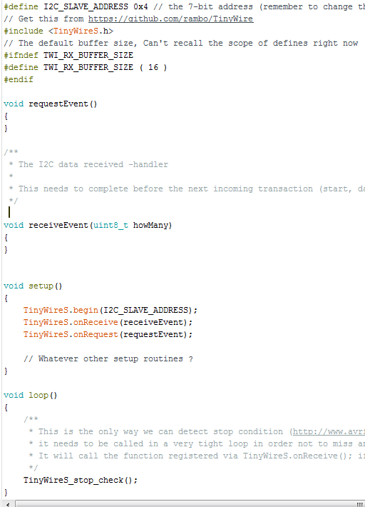
I then moved on to modify the code to turn an LED on Pin 7 on and off depnding on what is received.If the byte 0x1 is received, the LED turns on. anything else, it turns off. I also programmed in checks to see if the number of bytes received is 1, since that is the number of bytes the slaves should be receiving.
I then programmed each board using a FabISP, remembering to
change the address from 0x1 to 0x2 in between. The boards should be ready to use, but first I need to program the master board.
Programming the Master
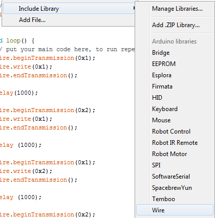
Programming the master board was more straightforward. The 328 already has a library avalible in the Arduino IDE, which is easier to implement.
To program the master board I first had the I2C on the master begin transmission, transmit 0x1, the end the transmission. I then had the 328 wait 1 second. I copied this block of code 3 times, first to change the adress and then to send 0x2 to both to turn the LEDs off.
You can see some of the code in the image above. Note that I used the modified boards and avrdude files from Output Devices to program. The normal files can be used if you have a 328P intead of the 328.
Of course, when I tried to program the 328 with the FabISP, it gave me the rc = -1 error code. The first thing I did was check the resistance of any of the traces. leading from the ISP header to the chip. A high resistance would generate this error. None of the traces appeared to generate high resistance. I then checked wether or no any of the traces were shorted together. This PCB was not completely finished in the solution and I needed to go through the board manually with a razor. I may have forgotten some spots. None of the ISP pins seemed to be shorted together. I then defaulted to resoldering all of the pins. That didn't work, so I then checked my board layout and...
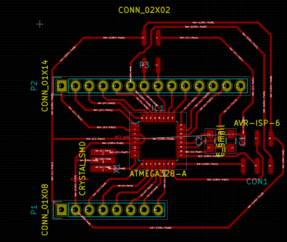
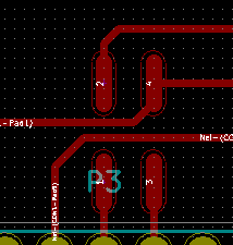
If you look closely, you will see that the vcc pin of the 328 is connected to the gnd pin of the chip, and the VCC pin of the ISP is connected to nothing. Since the VCC pin is connected to nothing, the chip did not receive power. I should have checked the voltages on the board before resoldering. I must have assumed that the VCC was already connected whan I finished the board. I fixed the issue (again with no extra parts) and re-made the fixed board. Below you can see the correct rearrangement of traces around the I2C header.
After making the new board, I programmed the new main board with the code, and connected the two slaves up. It worked perfectly, except the sencond LED didn't work properly. I reprogrammed the main board's bootloader and both boards worked perfectly.
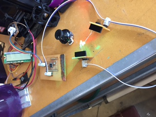
However, I felt that the timing was off so I uploaded the bootloader to the master and the timing was proper again. My I2C communication now works for my final project.
Files
 - Main board
328I2CNodeLaseFixedAgain.ai - Adobe Illustrator file for the main board
ReceiveTinyReal.ino - Code for the receiving slaves
SendMega328.ino
- Code for the main board
328I2CNumbers.zip - KiCAD files for main board
Files for the Tiny I2C Nodes
can be found in Input Devices