Electronic design
Assignment for week six (March 05, 2014)
The assignment of week six was to redraw and make the echo
hello-world board, adding a button and LED. I refered to the
tutorial by Anna Kaziunas at
http://academy.cba.mit.edu/2012/labs/providence/tutorials/07.html
1. Downloading Eagle 6.5.0
- Went to http://www.cadsoftusa.com/downloads/
- Downloaded eagle 6.5.0
- Installed freeware on Linux
2. Downloading echo board and schematic
- Downloaded the files from the link on the tutorial page
mentioned above
- Extracted the file on my home directory, in Ubuntu
- Opened eagle
- The helloecho folder was visible under "projects" on eagle
- Ensured that the little dot on the right side of the libraries
were green, by right clicking on it and checking the "use"
3. Downloading and installing the
Libraries
- Downloaded the libraries from
http://academy/cba.mit.edu/2012/labs/providence/tutorials/Downloads/eagle_libraries.zip
- Installed them using the sudo apt-get install command
- Unzipped the files
- Ebsured that the little dot on the libraries was green
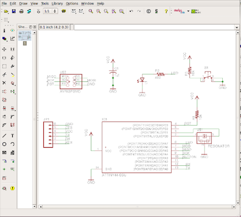
4. Editing the schematic
As I had prior experience in using eagle, it was not that
difficult editing the schematic. I added the LED, button,
resistors and a capacitor. I connected all the newly added
components and ensure that they did make a connection.
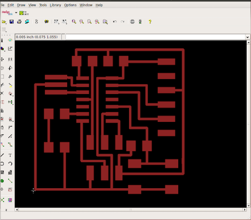
5. Designing the Printed Circuit Board
(PCB)
- Once the schematic was completed, I switched to teh board view
- The components which were added were visible, with yellow
unrouted traces attached
- I moved enlarged the board outline in order to move around the
existing components omn the board, to make space for the newly
added components
- Once the components were placed, I then routed all traces,
however I used the manual routing instead of auto routing
- Checked errors on the board, using the Design Rule Check
- I changed the board outline width from 0 to 0.01 width to make
it wider
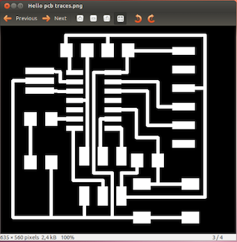
- I exported the circuit traces as png file, as per tutorial
(monochrome, 500dpi)
- Then after, I exported the board outline, as per tutorial -
using the same settings as above
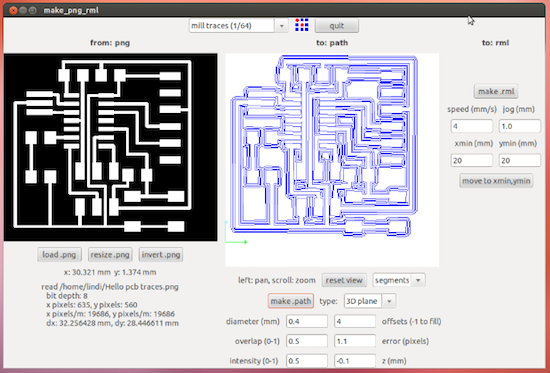
6. Importing the files into
Fabmodules
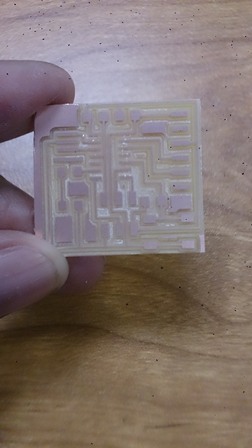
- Firstly, I loaded the traced png file on fabmodules and milled
out the board
- Then, I loaded the cut-out png file to cut out the board
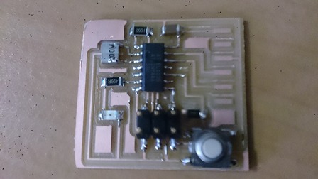
7. Populating the board
- Once the milling and cutting-out of the board was completed, I
soldered the components on the board.
- The image of the soldered board was taken prior to the 6 pin
header soldering