 Fletch's Fab Academy 2014 Blog
06. Electronics Design
This weeks assignment was to:
- Re-draw the basic Fab Hello World board, adding a button and
LED in the process.
- Check the design rules.
- Make the board.
- Extra Credit - Simulate the board.
06.01 Re-Draw the Board
As the existing board is so simple I thought that it would be a good
exercise in Eagle to start
from scratch with a blank project and work through the whole
process. I used the existing partial
board design, the ATTiny44 data sheet,
the fab
invetory and an actual check of the contents of the draws by
our Fab Lab electronics workbench as a starting point.
Once I understood what components we actually had available the next
thing was to find suitable libraries for them. There seem to
be a couple of copies of differing generations of FabLab Eagle
libraries around, however the ones linked from this
tutorial seem to cover most of the components required. I'm
using a Mac and installing the libraries is slightly
'non-maccy'. Basically there is an Eagle folder in the
'Applications' folder, this contains a 'library' folder where you
should drop the new library files.
My completed schematic looked like this:
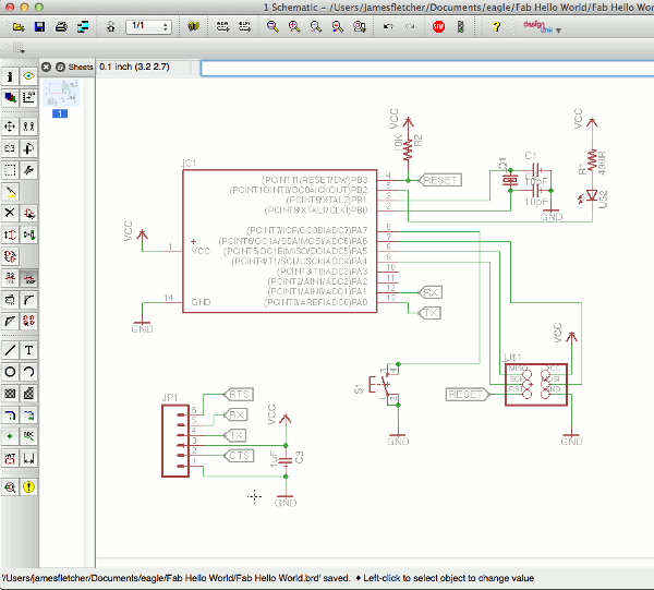
Notes:
- I've connected my LED differently from the tutorial. I
prefer to use the micro's IO pin to sink current rather than
source it as most micro's will sink significantly more than
source. The ATTiny datasheet claims symmetrical sink and
source currents for IO pins, but old habits die hard.
- My button connects to ground and I use the internal pull up
resistor in the ATTiny rather than the external one used in the
tutorial.
- I've used different IO pins for my LED and button from those
in the tutorial. This was just to make it easier for me to
route the board.
- I've decided to use a crystal and pair of 10pF caps rather
than the resonator.
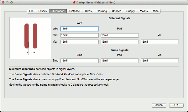
Next I created a new set of design rules in Eagle. Based on
the 1/64th (0.015625) inch tool size that we use to mill the traces
on the Modela I decided to set the minimum clearance to 16mil.
I also decided to use this for the minimum trace width, although
this could well be smaller.
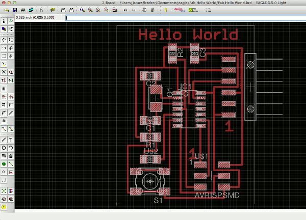
Initially I tried to use Eagles auto router, however it only managed
to route 75% of the board and left me with some real conundrums for
the manual routing. So I eventually ripped up all of the
traces and started again with a completely manual routing
process. After a few attempts I managed it with no 0R jumpers.
06.02 Check the Design Rules
I then checked the board against my Modela based set of design
rules. Bang! Loads of errors. Most were inocuous,
however the major issue was that where I had run three traces down
the center of the ATTiny44 the DRC was complaining about the
clearances between the traces.
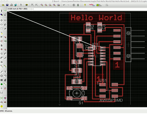
I should really have modified the board at this stage, but looking
at the example board layout in the tutorial and at another board
here in the lab I decided tha there was space for the three traces
and that I should just see how the board would come out. So I
followed the tutorial to export the traces and interior PNG file for
milling.
06.03 Make the Board
Once on the Modela I used Fab Modules to create the tool paths,
however where I had the DRC clearace issues no tool path had been
created as the tool was too wide to fit. I had two choices:
- Go back the Eagle and tweek the traces to space them perfectly
down the center of the ATTiny44. The correct choice!
- Nobble the tool size in Fab Modules to make them believe I had
a smaller tool that would be able to mil the design as is.
I decided to try option 2. By reducing the tool size from
0.4mm to 0.3mm Fab Modules created a tool path that separated the IC
pads from the traces. Whilst not ideal, I had faith that for
this quick test this would work OK. The tool would be centered
in the correct place, but would remove 0.05mm more material to each
side than fab modules expected, slightly thinning all of my traces
and component pads.
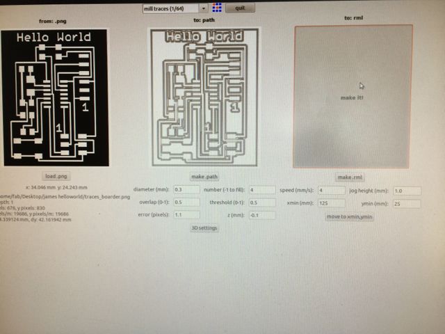
This actually produced a surprisingly good board.
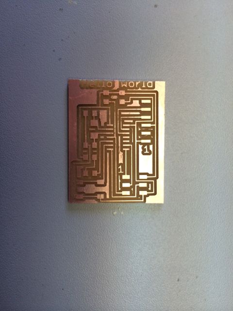
The only real issue is that I could have left more space around the
outside when creating the interior.png file so with the 1/32inch
tool used it's actually chopped off the top of my text.
Next job was to populate the board.
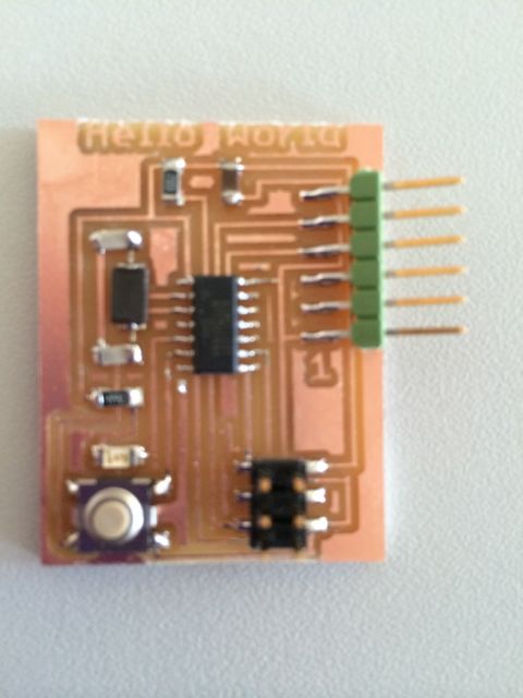
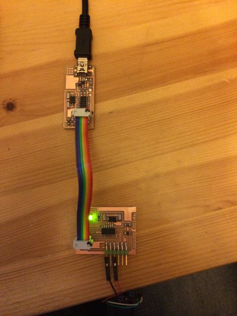
06.03.5 Test!
I wasn't happy about not being able to test the board for 2 weeks,
until we did 'Embedded Programing', so I decided to put together a
really quick and dirty test program, this would also give me a
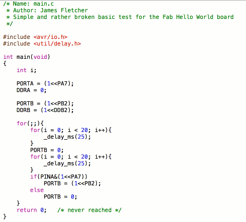
chance to work out how to use the 'Crosspack' AVR tools on the
Mac. The code below isn't pretty, it flashes the LED until the
button is pressed, at which point it leave the LED on. I left
the TTL serial interface tests, as there was little that could go
wrong here.
I programmed the board with the Fab ISP we made two weeks ago.
Eagle sch and brd files.