 Fletch's Fab Academy 2014 Blog
This weeks task is to make a 'FABISP In circuit programmer'.
We'll be using this device extensivly in later weeks to program our
embedded electronics.
The task doesn't require any creatrive input from us, the designs
are all provided. This week is really all about learnig the
work flow and learning to use the Modela micro milling
machine. However there are a lot of steps to the machining of
the PCB and final manufacture, so there is lots of scope for errors
and it could be quite a time consuming task. For the most part
I followed this excellent tutorial: http://fabacademy.org/archives/content/tutorials/05_Electronics_Production/Assemble_and_Program_FabISP.html
04.1 Workflow
04.1.1 Decide what to actually build!
There are 2 varients of the FABISP, one with a crystal and one with
a resonator to clock the ATTiny44A micro. After a quick check
of the parts available in the Manchester FABLab inventory I decided
to build the crystal based version as the timing for the software
USB implementation would be more accurate.
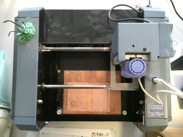
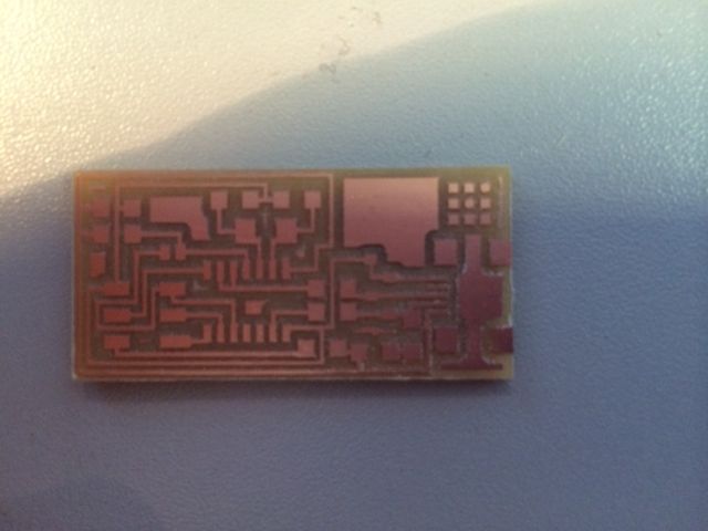
04.1.2 Use the Modela micro milling machine to mill a PCB
We start with a plain piece of copper clad FR1 PCB and a .png file
showing the pcb traces. Stick the blank PCB down with double
sidded tape, but make sure that there is some sacraficial material
under it, so that when we finally cut the board free we don't mill
into the machine bed and damage it or the cutting bit. It's
also very important to clean the bed before sticking down so that
our PCB material is completely flat. Our PCB traces cut is
very shallow (0.1 mm) so any hight discrepancy of this order will
cause the bit to cut too deep or fail to cut at all in some areas.
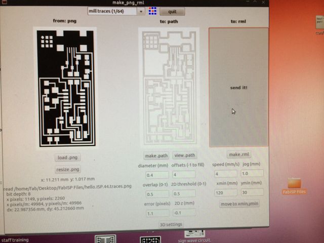
We then select the correct fab module (png to rml) and use the
software to control the machine and mil the PCB as follows
(following the steps from left to right in the fab module):
- Load the .png file.
- Select the type of job 'mill traces (1/64) - this pre-selects
some sensible defaults for cutting PCB traces based on using a
1/64 inch end mill bit.
- Make the PNG into a tool path based on the job type selected
above.
- Set the x,y origin for the area we want to mill so that it's
on our blank PCB stock. This requires a few iterations of
measure and using the 'move to' button to get right.
- We the set the z origin by moving the bed of the machine up
and dropping the bit down in the chuck so that it just touches
the surface of the PCB.
- Finally once the x,y,z origins are set we make an rml file and
send it to the machine
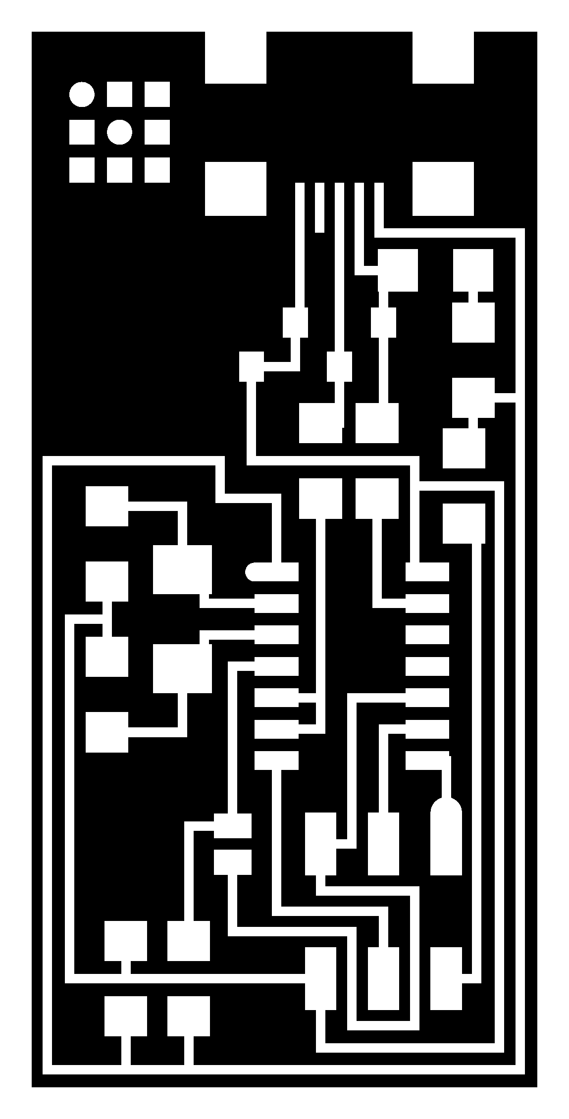
It takes about 10 minutes to mill the traces and you endup with
something that looks like this:
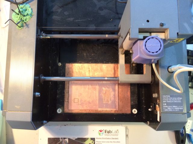
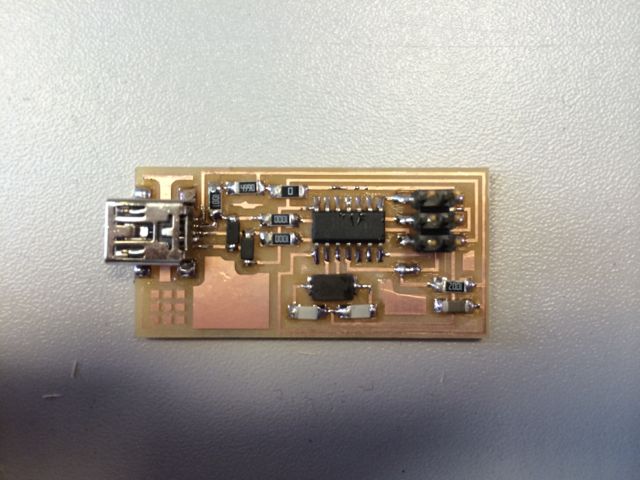
Once the traces have been milled we change the bit in the machine
for a larger 1/32 inch one and repeat the whole process for the
board outline .png to seperate our actual PCB from the stock,
finally ending up with this:
A quick gentle de-bur with a steel ruler and wash with soap and
water to remove and residue and trhen we can populate the board.
04.1.3 Populate the PCB
A steady hand and desk magnifier are required! The only
component that I had problems with was the Mini USB connector, the
ones in our inventory have a metal overhang at the back of the
connector that partially shrouds the pins and makes access during
soldering difficult. I'd recommend finding a different
manucaturers connector in future.
04.1.4 Test
- A quick visual inspection under the magnifier convinced me
that I hadn't got any obvious shorts and that it would be safe
to connect to my laptop.
- Then plug into my laptop via USB and check for blue smoke!
- Finally check that I had 5v between the VCC and GND traces on
the board when connected showed that I was at least in with a
hope of continuing.
- It may have been possible to use a scope to check that the
ATTiny OSC was running, but without checking the data sheet I'm
unsure if the initial chip config causes the OSC to run.
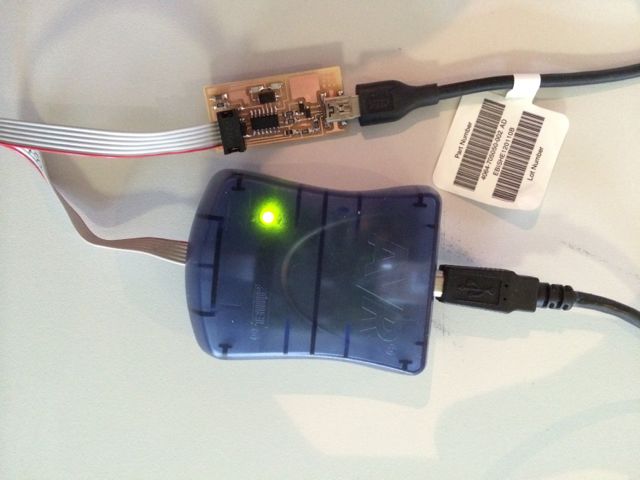
04.1.5 Program the FABISP
Again following the tutorial, I connected both solder jumpers on the
board (one requires a 0R resistor as it actually bridges a track)
and then used an AVRISPmkII to program. Note I had to connect
the ISP connector the other way around from that shown in Anna's
tutorial that I was following.
Also note that I got a single warning about function in-lining when
I complied the FABISP firware.
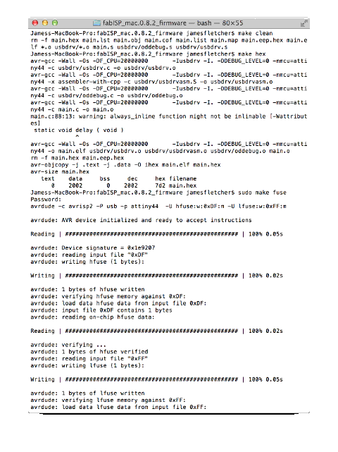
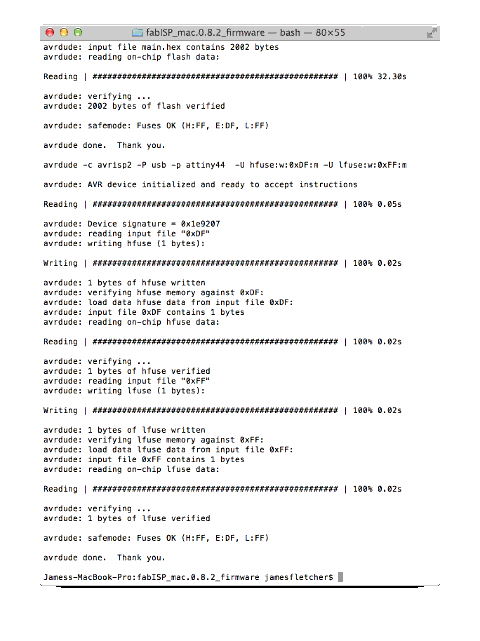
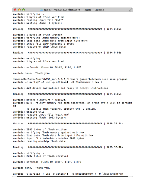
Once I had successfully programmed the device it appeared as
'FABISP' in my Mac system report. I then removed the two
solder jumpers.
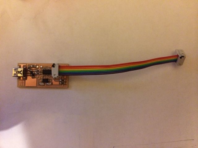
Here's a picture of my finished device with black dots marking pin 1
on the ISP connectors.
04.2 Problems with the Modela
The only issue we had was that at one point the Modela and the PC
driving it got out of sync for one of our students. We had to
delete the 'print jobs' from the controlling PC and then reset the
Modela. To delete the jobs run:
ps -aux
And identify the two processes that need to be killed. One is
called something like 'rml_send' and the other is 'cat fab.......',
they should have consecutive process numbers. Then kill each
process by number with (e.g. process number 2266):
kill -9 2266