4. Electronics Production
Index
- Assignment
- Introduction
- Rolland Modella MDX-20 Our machine
- Making of fabisp
- Choosing the design
- Working with fab modules
- Setting up the machine and milling the board
- Soldering
- Soldering Step by Step
- Soldering the IC
- Soldering other components
- Pitfalls
- Programming the ISP
- Issues faced
- Summary
A. Assignment
- Make an in-circuit programmer by milling the PCB
B. Introduction
Once in my school days i remember trying to make a pcb and soldering things up. It was a
hard
time
with all those chemicals, glooves and those wastage of boards. It was good to see that things have
changed, at
least there
are other options coming up for PCB production. Traditionaly to make a pcd you need to screen print the
circuit
and place it
on the board and heat it with an iron so that the ink sticks to the board.After that You need to place
the board
in an
iron chloride solution( etching solution). During this the copper, more reactive compared to irom
replaces it
from the
ferric chloride forming copper chloride. Thus the copper gets dissolved in ferric chloride. Now as we
have
masked
the places where we want the copper to stay. The contact is prohibited for ferric chloride. Thus in the
regions
where it
is masked reaction does not take place and we get the printed Circuit Board. This was quite messy and
time
consuming.
I was really exited to see the milling machine and how it can be used to mill out the copper from a
board to
make a PCB.
No chemicals! No Heating! and no Lengthy procedures.
c. Rolland Modella MDX 20- Our Milling Machine
We use Rolland Modella MDX 20 in our lab.
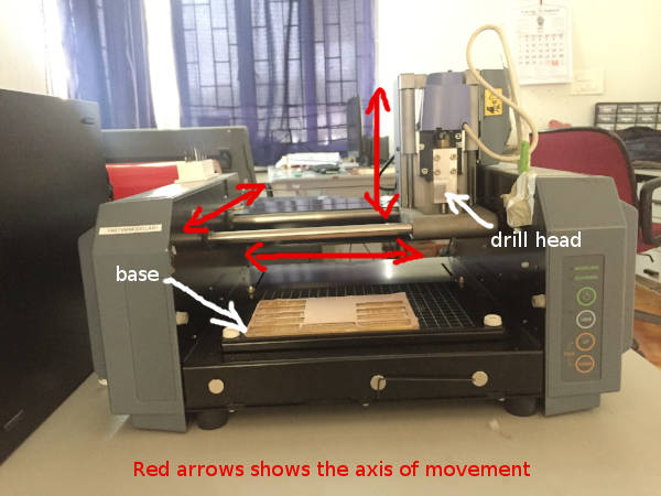
Rolland Modella MDX 20- Our Milling Machine
This machine can be used to mill a copper cladded board to make a pcb and
wax to make molds for molding purpose. This week we where introduced only to PCB milling part. It was
our
assignment to make a ISP (In System Programmer) which is used to program micro controllers.
Let me take you through the machine and its working. It is a 3-axix machine. It has a drill attached to
a 2 axis movable fixture. That means the drill can be moved along a plane. Now the drilling arm itself
can be
moved up and down. We can place different end mills in the arm depending upon the width you want to
mill away at a
time. End mills are available in the following sizes
- 1/64th of an inch
- 1/32nd of an inch
- 1/16th of an inch
- 1/8th of an inch
We use
- 1/64 end mill- for milling away the copper
- 1/32 end mill - for cutting the copper baord
End mills
D. making of fabisp
D1. Choosing the design
Before i start using the machine, i had to choose from different ISP designs which i
want to make. These ISP's are called
FABISP
as these circuits and designs are opensourced by the fab team. I choose Brians
design as it had a couple of LED's one to indicate the power and other indicating flashing. I belive as
a amature these indications are of great use while debugging.
The design and the circuit diagram where all provided in the website. All we had
to do was
to download the traces and the board outline files in png format to get started. The images are shown
below.
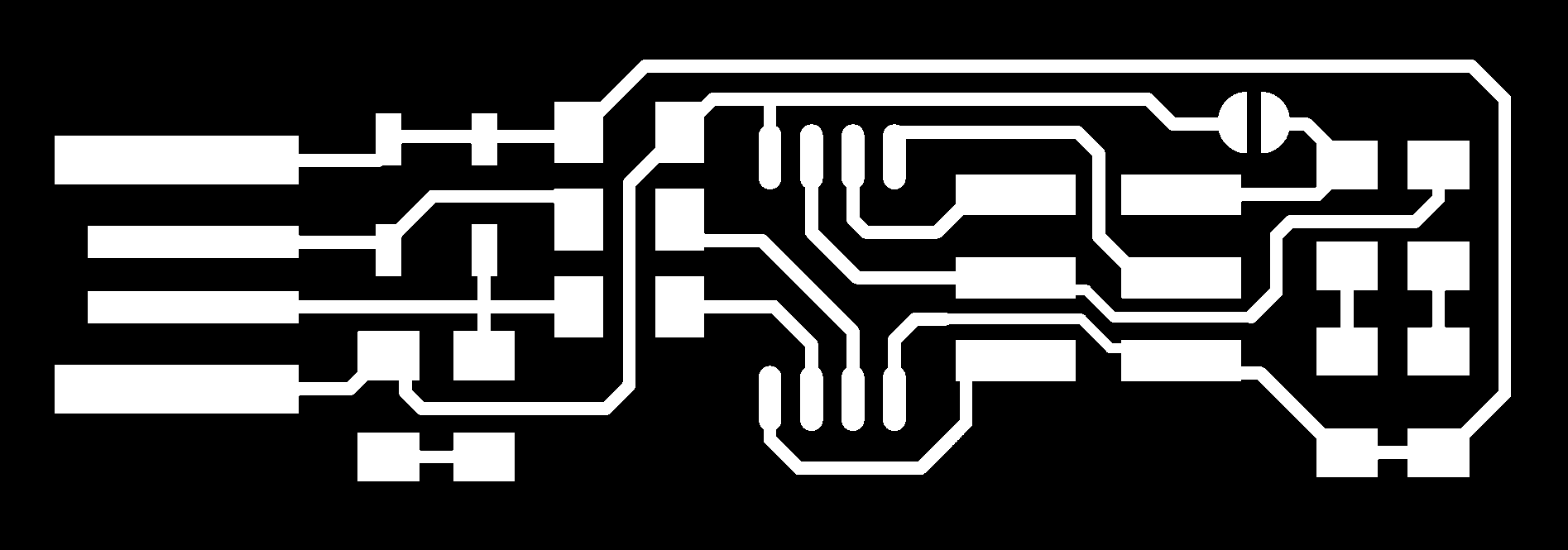
Traces image

Cutting Image
These images are designed in such a way that in the traces image the
white parts represent the region where
the copper need to be retained and the black is the region where copper needed to be removed. In the
cutting image the black and white junction is where
the cutting happens. A path is drawn in the intersection of these two colors and cutting happens through
these paths.
Remember that in the cutting image if you put white outside and black inside then the machine cuts to the inner side. This can sometimes
go over your traces. Thus make sure that you have black outside and white inside for peoper results.
D2. Working with fab modules
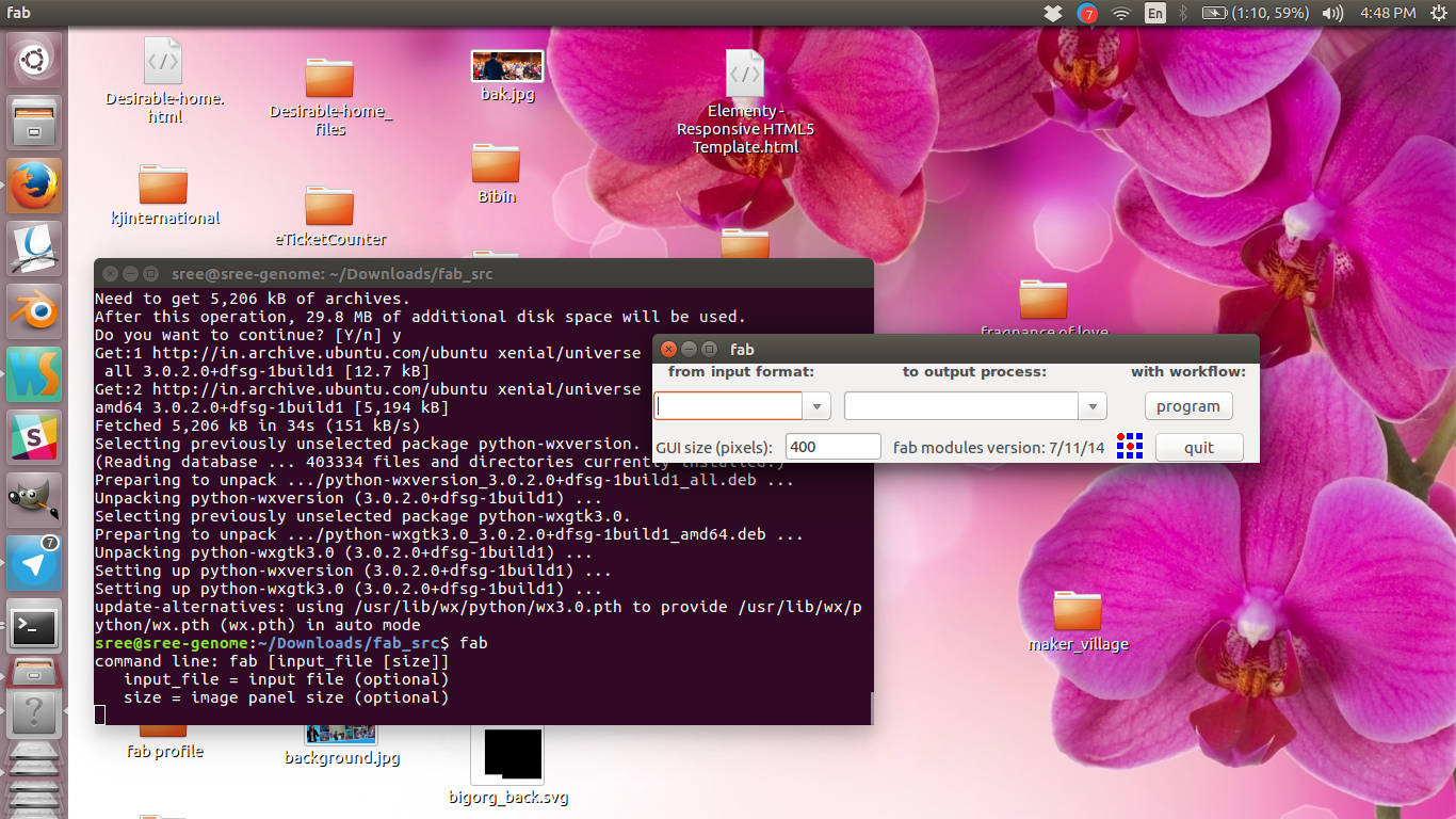
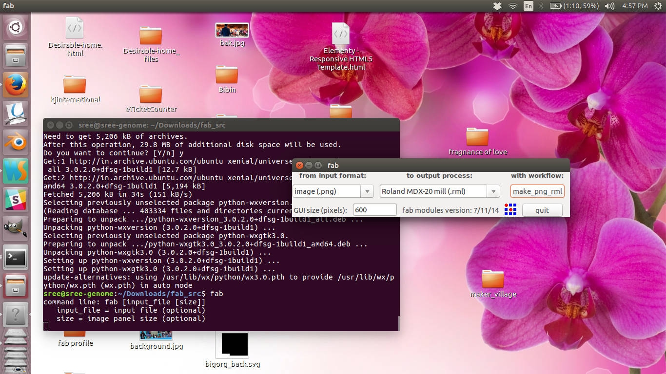
Once you have your images ready, you can install fab modules if not installed already. Steps to install fab modules can be found here. Once you have the modules installed you can launch it by typing the "fab" in the terminal click enter.
You will see the following UI showing up.
Fab modules initial screen
Now choose input as png and output as roland rml and click make
png_rml.
 Choosing input and output formats
Load the traces image into the ui and choose end mill size to be 1/64
from
the top dropdown.
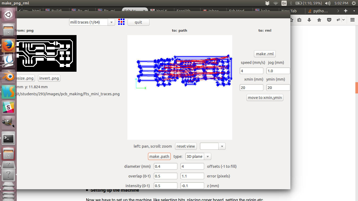
UI for milling
There are different options in the ui.
- Diameter: Diameter of the end mill
- Overlap: How much the bit overlap in adjuscent paths
- Offset: It determines the amount of copper milled out
- Error: Pixel approximation while creating vector path from png images. Less the error smoother the paths
- Intensity: Power
The default parameters are good enough for the go. Once you are done
click on the make .rml button. You can see a new "send it " button appearing and the time taken for the
process is shown up.
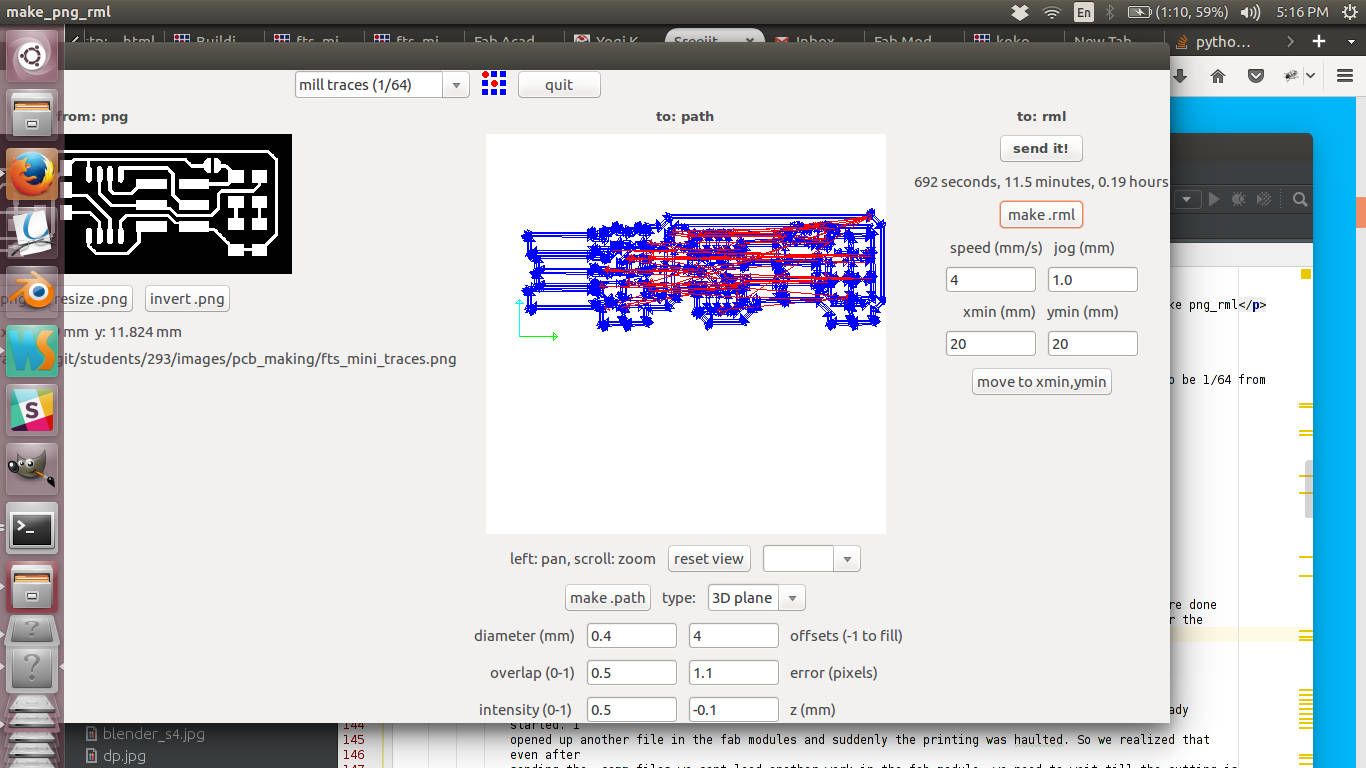 Send it button and time of milling.
d3. Setting up the machine and milling the board
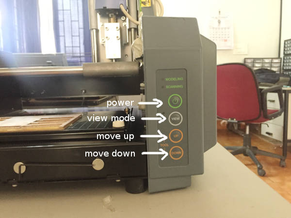
Milling machine controls.
Turn on the machine and put it on the view mode by clicking the view button.
You will notice that the base moves outwards so that we can place and fix the board on the base.
Now we need to place the copper cladded plate sicked on to the base plate of the machine
with a double sided tape and make sure that it is perfectly horizontal and even everywhere. Our base
plate
was having a pcb already sticked on to it so that it can act as a sacrifactial layer. So we sticked our
plate
over this layer
Go back to the printing mode by clicking on the view button again.
The drill moves and position itself to a default position. The drill head will be at its top most
position.
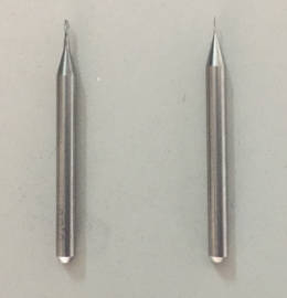
Now insert the 1/64 end mill into drill head, and make sure that 70% of the bit goes inside the head.
We use an Allen key to remove and
fix the end mills
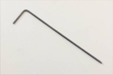
Allen key.
By trial and error position the drill in the exact portion where you want it to be.
This can be done by changing the x and y offset in the ui and clicking move. Once you have the drill
positioned in the
exact location you want it to be, its time to adjust the end mill so that it just touches the surface.
First we have to pull the drilling head down such that there is only the thickness of the board left to
move
downwards. Now loosen the end mill using an Allen key such that its tip touches the plate. now tighten
the screws properly
.
Press the down button once and you will find that a bit of drilling happens and material is thrown
out.
Now we are ready to mill the board. Click on the send it button and you will see the machine starting to
mill our
board. It will take a few minutes to couple of hours depending on the size and the milling operation to
be
performed. Before you start the drilling operation make sure that you have noted down the location on
the
drill initially because for the cutting operation you need to start exactly from that point for proper
results.
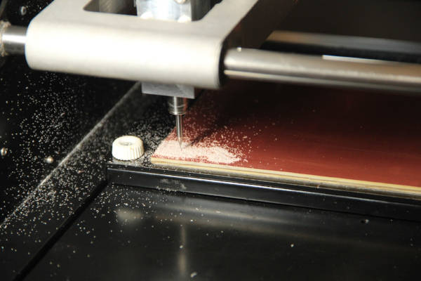
PCB milling
PCB after milling
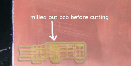
Once you are done with the milling, its time to cut the pcb out from rest of the
board.
As before load the png cut image and pick 1/32 from the top dropdown, few settings will appear and we
are fineo go with that. Once we are
oky with the settings move the drill head to the exact position where we started the milling operation
from. Do the other procedures of
setting up the machine and end mills as in the milling operation. Once you are done click the send it
button and we will see a progress bar
in the screen and the machine will start the cutting operation. After the process remove the dust with a
vaccum cleaner and remove the PCB
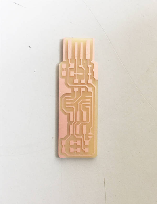
Final PCB
d4. Soldering
We use SMD(Surface Mound Devices) for our project. First the components where identified from the website and was written down to a paper. From the inventory in the lab these components where identified and sticked on to the paper corresponding to there names using a double sided tape. It is very essential to do it this was as the components are very small and the labelings are hard to read. So if you mess up with these items you are going to waste a lot of time figuring out which component is which. So always be careful while picking comopnents from the inventory and do stick them to the paper corresponding to there name.
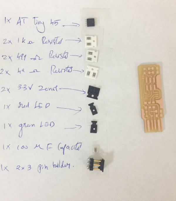
Inventory for soldering
I had to refer a couple of tutorials on soldering to get started. Though i have a hands on experiance on through hole soldering, i am new to SMD solidering. These tutorials helped me out. How to SMD soldering , though all the tools shown in video is not available in our lab, it is a good tutorial to get a concrete idea on how to do it
The main tools in our lab is shown below.
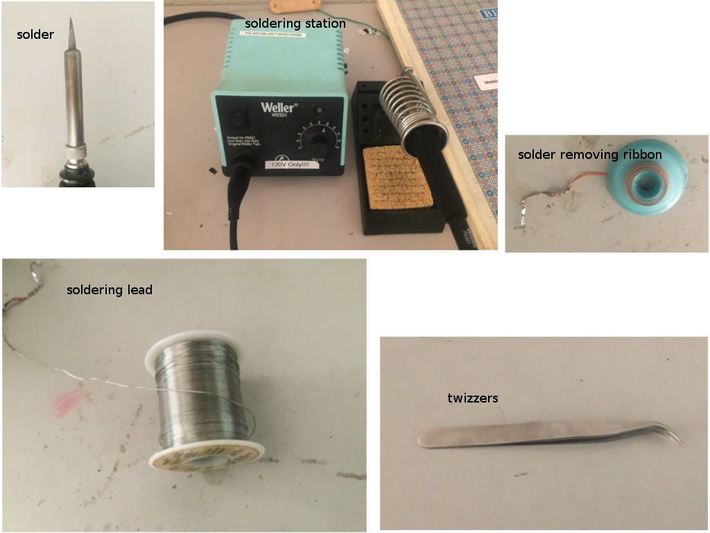
Tools
One important thing missing in the image is flux.
It comes handy to clean the board and when you find that the soldering lead does not
stick into the pads.
e. Soldering Step by step
e1. Soldering the IC
It is a good practice to start with the bigger components while soldering.Here the IC
is
the biggest component, so lets learn to solder it first.
- set the temparature in the soldering station to around 600 to 700 farienheit
- clean the pads with flux
- Place the ic on the pads such that all the legs are placed correctly on the pads and there is equal margin in the both sides. There should not be any rotation of the chip.
- With the soldering iron, melt a little bit of soldering lead and take it in the tip of the solder
- Now touch the solder tip with the soldering lead on any of the corner legs of the IC. You will see that the lead flows down and covers the leg and the pad joining them
- If you find that the ic is not aligned properly then touch the iron tip on the same leg for a while making the solder melt. Now slightly adjust the IC to bring it in place.
- Now you have your ic properly in place, you can go ahead with soldering the diagonal leg. Folow the same procedure
- For the other legs follow the style of soldering shown in the video, where we place a big amount of solder on one leg and streak it to the other legs utilizing the surface tension of the soldering lead.
- After completing soldering of all the legs you can touch each leg with a clean soldering tip so that the soldering lead can melt and distribute evenly, this will give you better results.
- Once you are done you can remove excess flex with a piece of cloth.
Method 1
- set the temparature in the soldering station to 750
- clean the pads with flux
- Touch the solder tip on one of the corner legs of the ic pads, this will head the pad
- Touch the soldering lead on this pad, the lead melts and fills the pad
- Place the IC on the pad properly aligned, you will notice that one of the leg is over the pad with solder
- Keep holding the ic in place and touch the solder tip on that leg corresponding to the pad with solder. You will notice that the solder melts and the IC moves down and sticks to the pad
- You need to solder the other legs using method 1
Method 2
e2. Soldering Other Components
Other components can be soldered in either method 1 or method 2 depending on your personal preference. I prefer the second method
e3. Pitfalls
1. Sometimes while soldering there occurs bridges between legs of ic. TO remove them
put a little
more amount of flex in the area try heating it up. Use the wik to absorb excess solder. Now drag the
solder to remove
the bridges. Add more flex if required. This is well explained in the video above.
2. Don't heat the leg of a component for a long time or else you will burn that component
3. If you keep heating the pad for long time it may come out
4. Make sure that you connect the following pads with solder before moving on to programing.
Finally i have my pcb with components soldered to it
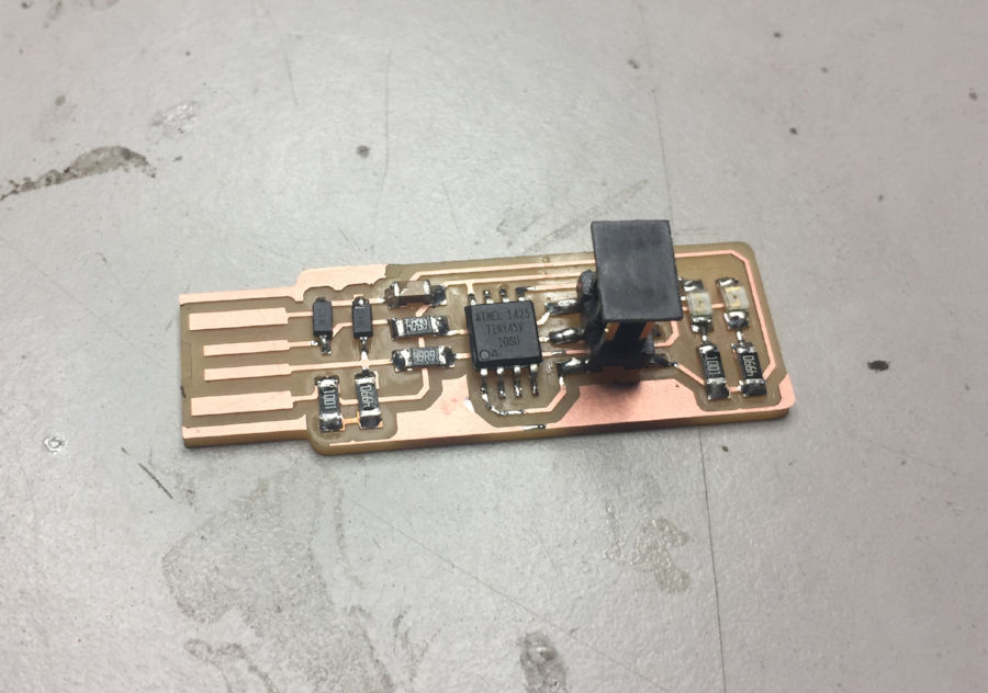
Final pcb with soldered components
f. Programing the ISP
Programing the ISP is also well documented at Brians website. The major steps are documented below.
- Software installation: In linux you need to run
sudo apt install avrdude gcc-avr avr-libc make
to install all required software, which include avr programming tools and libraries and make. - Download firmware: Use this link to download the firmware code
- Unzip the downloaded file: YOu can now unzip the downloaded file
- Run
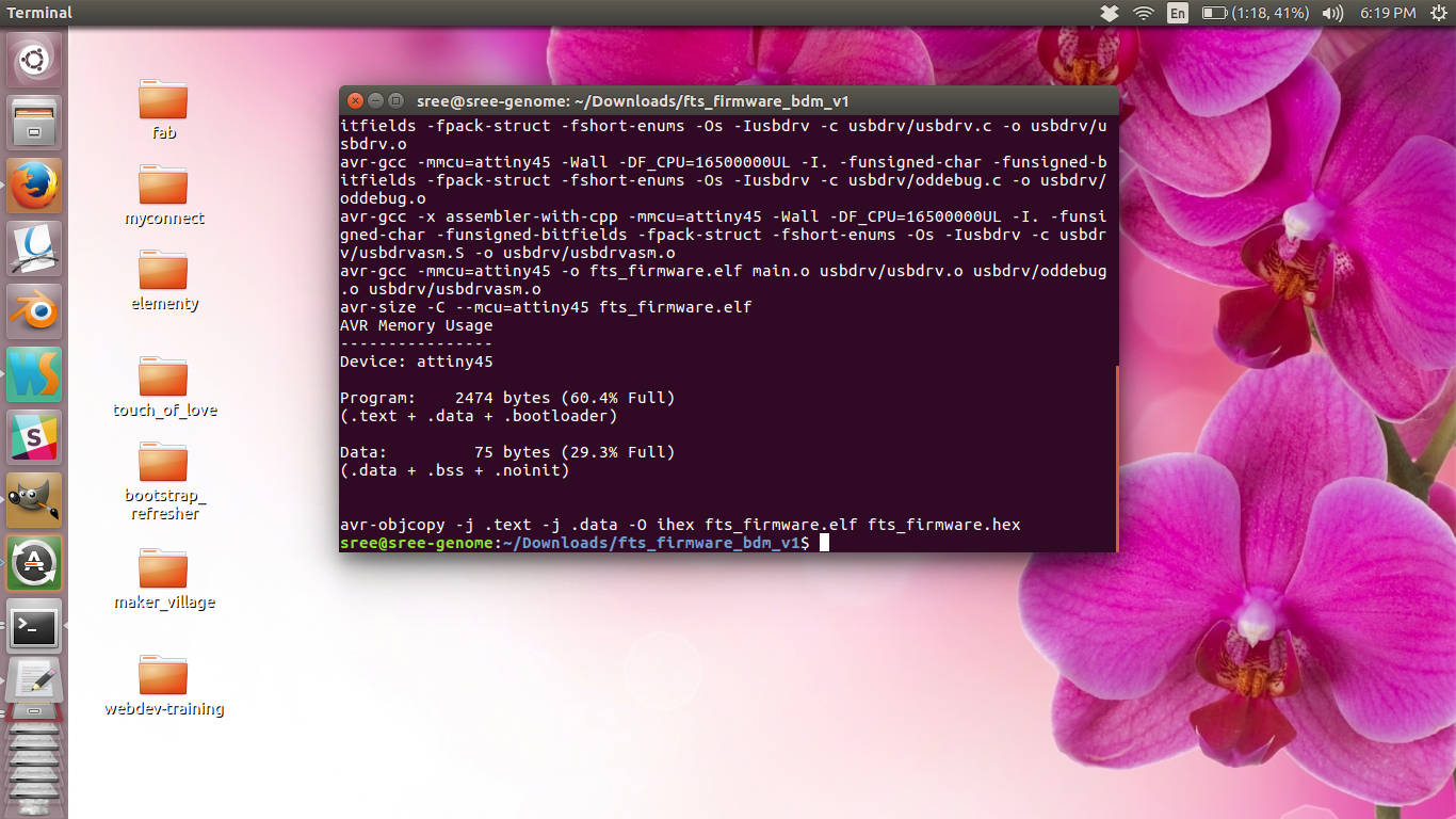
make
This will generate the .hex file. After completion you will get a file called fts_firmware.hex - Update MakeFile: Open the make file in the directory in gedit and near the top
find the line saying
PROGRAMMER ?= usbtiny
and change usbtiny yo the programmer you are using. I am using a ATtiny board so no need to change this. - Test by connecting to usb Now we can connect the device to a usb port and see if the red led glows. If it does things are good so far. It is recommended not to plug the device directly into the PC's usb rather you can use a short usb extension for this.
- You need to have another ISP programmer in order to program your board. I used Syeds ISP to do
this.
You need to plug the other ISP to the PC and then connect the isp cable from that to the new board. Once you have this connection is established you can move ahead and program your own board to make it as a programmer. - Erase terget chip now erase the target chip by typing
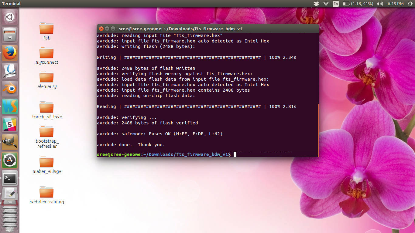
make flash
You will see some progress bars. If some error is shown try holding the connections tighty and try again.
- Configuring the fuses run
make fuses
to configure. Here we are burning the program into the MC, The program burned is to make the IC behave like a programmer, ie take the hex file provided by the compliler and burn it into the MC. It also does pulling up/down the reset pin based on the type of ic being programmed. For Attiny the programmer pulls the reset pin down to bring it to the programming mode and then flashes(burns) the program into it - Blow the reset fuse run
rstdisbl
With this we are disabling a fuse bit in the high fuse byte. This bit is specific to programming an MC. If we disable this fuse bit the MC will no longer be programmable. Here we are not planning to use the MC in the ISP for anything else other than to program other MC boards. This step also ensures that you dont accidently change the program in the ISP MC making it unable to operate as a programmer. - Test the ISP by pluging your isp into the usb port and type
lsusb
This command lists all the usb devices connected to our PC. This will help us see if the if our programmer is working properly. IF our devices is listed here we can ensure that it is working properly and all the steps we did is successful.
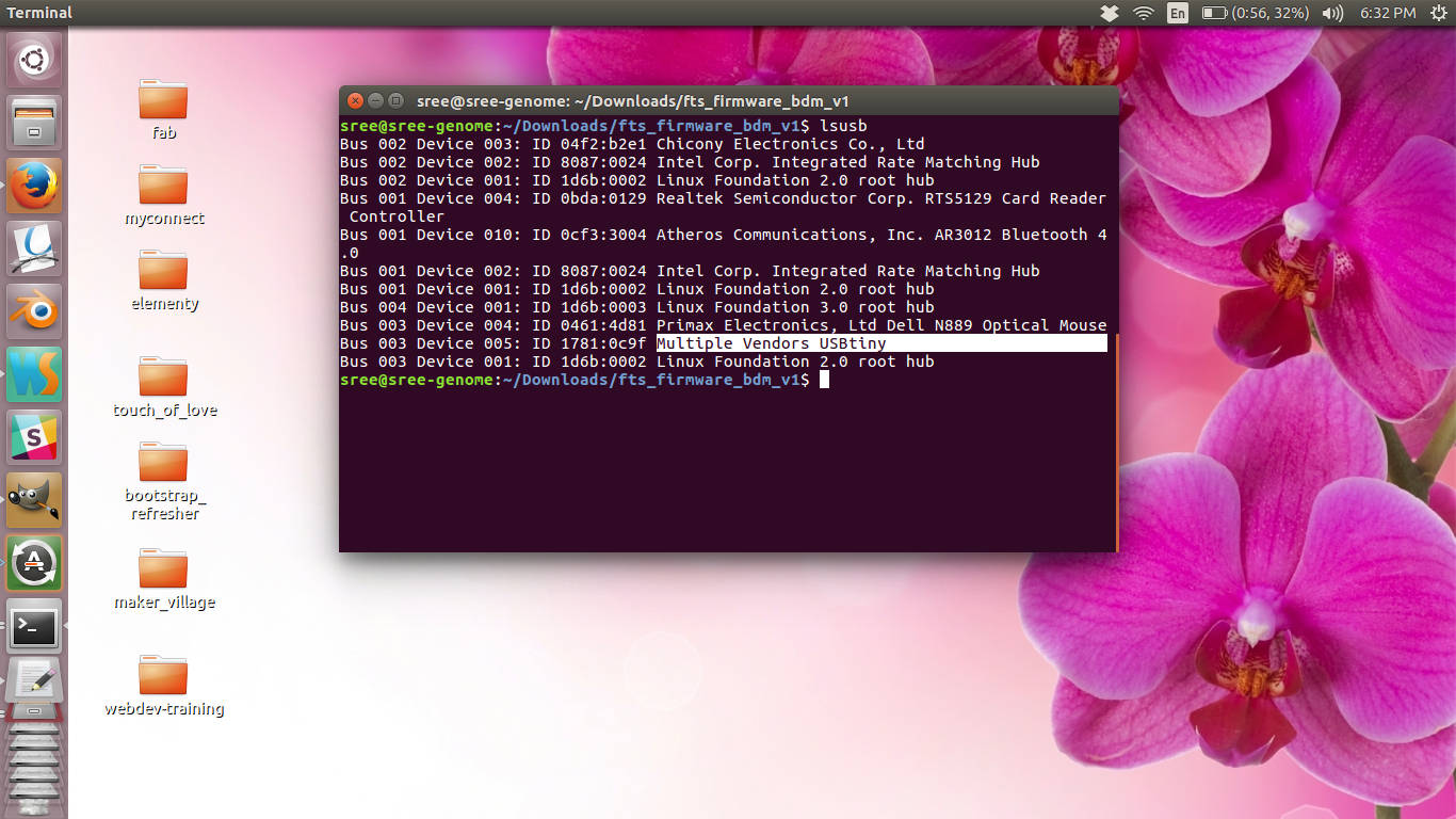
If it works properly you can see a "multiple venders usbtiny" in the list.
- Now your ISP is ready, you can use it to program other boards.
f1. Issues faced / Points to remember
- You need to put some extra solder in the usb connecting pads. If they are not proper you will either see the red led not lighting up or somethings blinking.
- After soldering check continuity to make sure that all the connections are proper
- Make sure that your connectors wires are tight enough.
- zenor diode and LEDs are polarity sensitive so make sure that they are connected to the correct terminals
- Alignment of the IC can be checked.
g. Summary
- Learned to mill pcb in Modella machine.
- Learned to use the fab modules
- Make my first pcb and soldered the parts
- Got a first hand introduction on how to program an avr microcontroller
- Learned to solder smd components
- Make my avr programmer and tested it.

This work is licensed under a Creative Commons Attribution-NonCommercial-ShareAlike 4.0 International License.