Our assignment for the week was to redraw the Hello Echo board and add an LED with a current limiting resistor and a Switch. Additionally we have to mill and stuff the board and see if it is working. If not we should try debugging it make it work and use the electronics testing equipments we have in our lab. We could also try and simulate the board. As Neil said the objective is to get used to many design tools and become familiar with all the testing equipments in our lab.
EAGLE is a electronic design automation application with schematic capture, PCB layout, auto-router and computer-aided manufacturing features. It widely used by many people and the learning curve is gradual. I found this software easy to use and has a lot of good features.
Eagle tutorials for Beginners like me.The first job is to Install Eagle. It was recently bought by Autodesk hence you need an Autodesk account to install Eagle. Once installed you need to add the Fab library to the Eagle.
Download Fab Library fab.lbr
The Fab library is a collection of all the electronics inventories available in the fablab. You will be designing using these components hence you need to have them in your library. You can optionally create parts of your own by drawing custom foots prints.
After adding the Fab library you can start drawing the schematic.
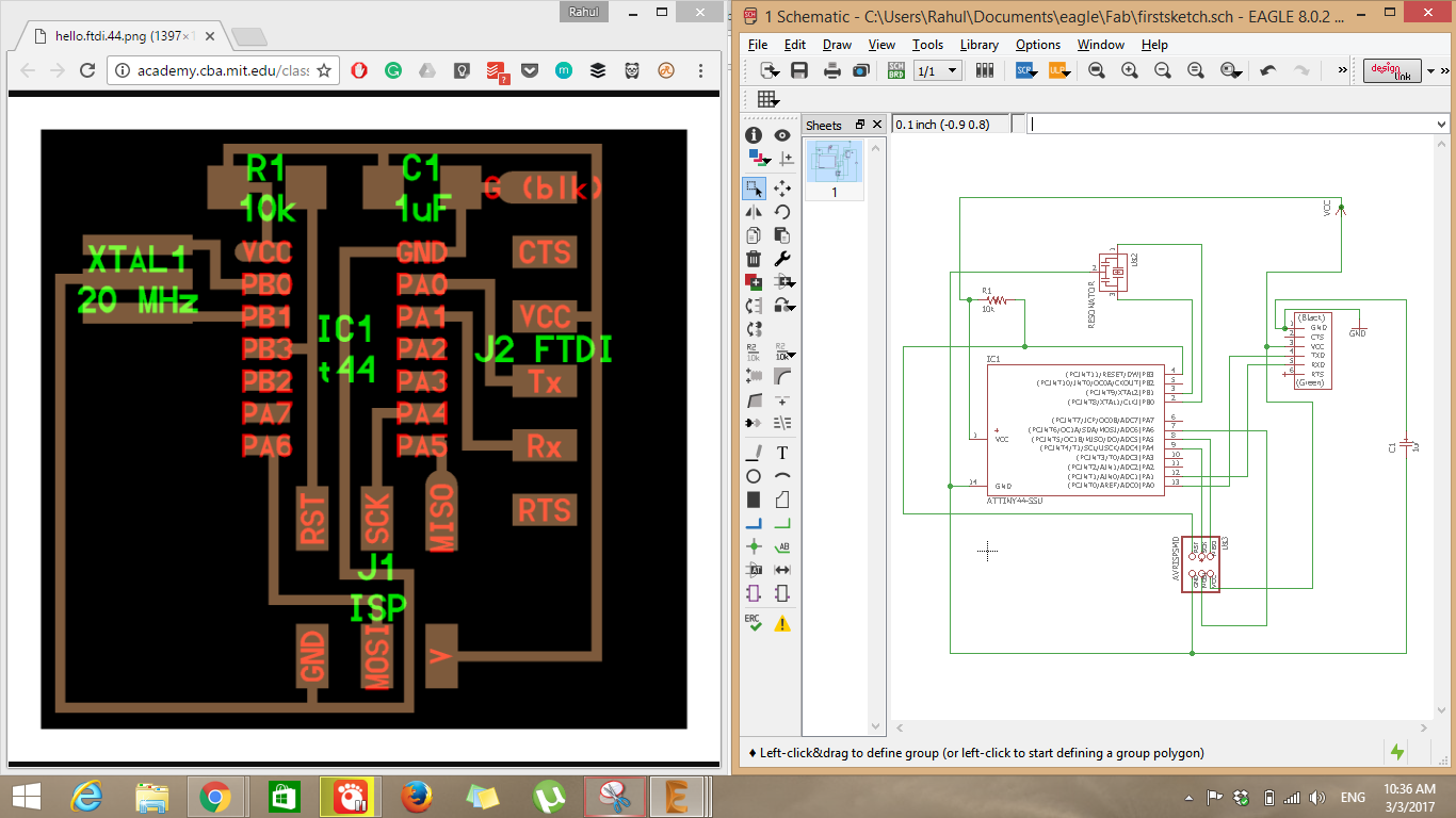
We will be using the schematic of the Hello Echo Board, and our task is to redraw this schematic to include an LED and a resistor.

Components Required
I started Drawing the schematic by referring to the original board design. For Drawing a board in Eagle the Steps are :
Common Problems
In some cases the Wire tool may not form proper connections, hence it is advised to use the net tool to connect different components electrically. Double check your connection to make sure that the lines do not cross over the component rather than touching them.
After one successful attempt, I remembered the Brian ISP programmer we the made a few weeks back, It has an 2 LEDs one connected between VCC and GND to show the power ON state. I wanted that functionality in my board also. Hence I started to change the schematic to include on more LED connected between the VCC and GND.
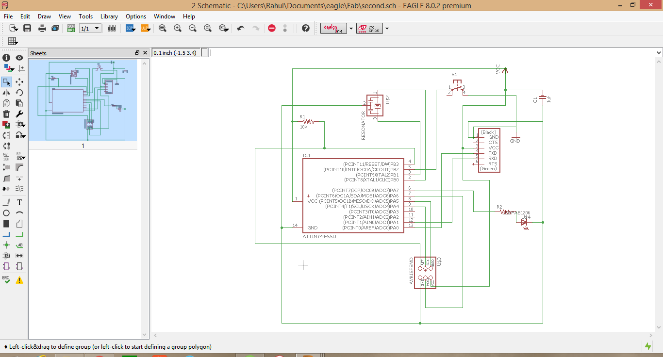
I added an additional LED, a current limiting resistor, and a switch to the schematic. The LED was connected between the PA7 pin and GND and the switch between PB2 and GND.
ERC involves checking a schematic for all the electrical connections. It will show errors, warnings etc. We can check this and correct the errors from the schematic. ERC will be displayed as a tiny icon in the bottom left of the page.
After Drawing the schematic you can switch over to the Board view by click on the top icon. In this view you can see the components and their foot prints and some yellow lines representing the connection you made in the schematic.
Before routing the board, the most important step you have to do is set the Design rules. The design rules relate to the trace width, the clearance between the traces etc.
The design rules can be set by clicking on the DRC icon in the bottom left corner.
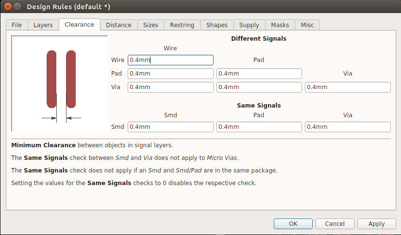
These are the default design rules in EAGLE, we changed all the value from 0.4mm (4mil) to 1.6mm (16mil) since that is the smallest end mill we have.
Next place all the components within the boundary. This is part which involves more thinking from your part, because the better the arrangement of the components, the better the routing.
This is the part where you use your awesome spacial acuity to neatly arrange the components and route the traces in between them.The objective is to reduce the size of the board and increase the packing density but still leave enough room to clearly isolate the traces an avoid any interference.
It takes practice to master the art of placing components in a board. You'll spend most of your time doing this. once you are done with this you can start routing the board.
You have two options when routing your PCB, Manual and Auto-Routing. What I found is that a good way to route your PCB is to do Selective Auto-routing. Wherein you auto route and get an idea on how the traces will go and then route them manually. This is a good method, it allows you to visualize the board first and then optimize the result the software is giving you.

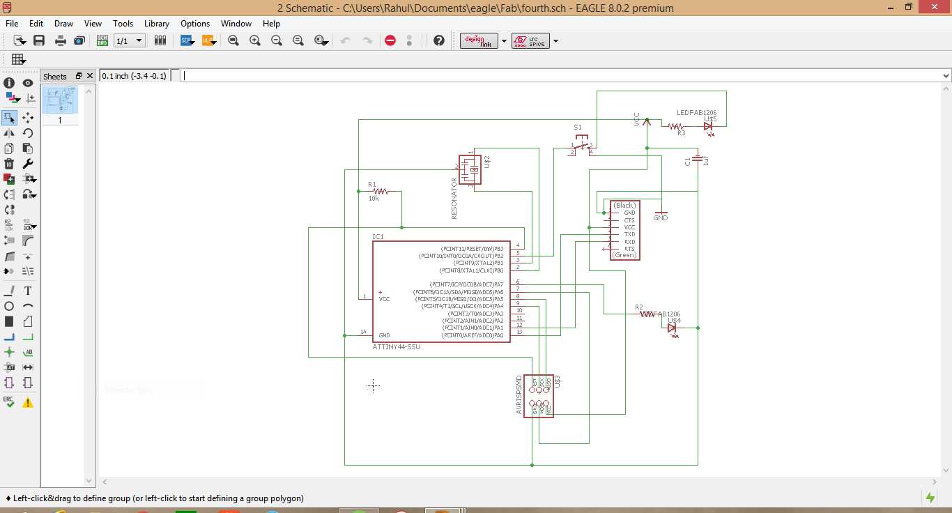
I rearranged the board again to place all the components in a neat fashion and used the Autoroute command to connect all the lines together. This did not work for my at first. After each Auto route I understood more about where to place the components better and after many iterations one was successful.
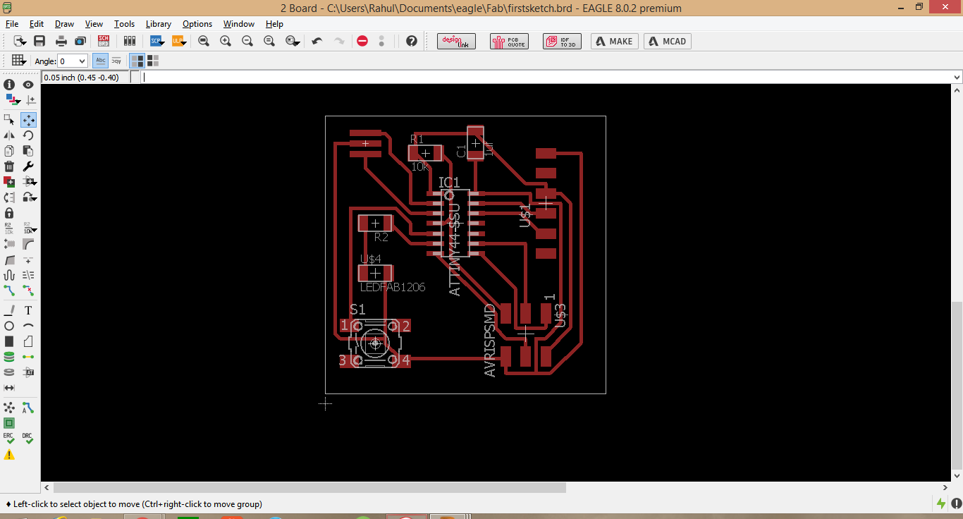

After a few Successful routings, I arranged the components a bit to make space for adding some text to the board. I wanted to write "Hello Echo"


This is the Final Board I designed with two LEDs and a SWITCH added to original version of the board. I found that there are two unused pins on the board which could be used for something productive. Hence I drew two additional pads and connected them to the unused pins. I'm happy with the design and EAGLE was a lot of fun to use. In the future, I will try more complicated designs.
I liked Eagle for its straight forward navigation and ease of use. The learning curve is gradual, You can learn to build circuits after spending about two days working on the software.
I tried this software for its ease of use. Anyone can quickly pick it up all the controls are intuitive, but it lacks all the functionality that EAGLE provides, which I kind of miss. The procedure is pretty basic. You add the components by clicking the insert component and you can search for the part you want, but the library is not extensive but it gives you the option to add your own parts.
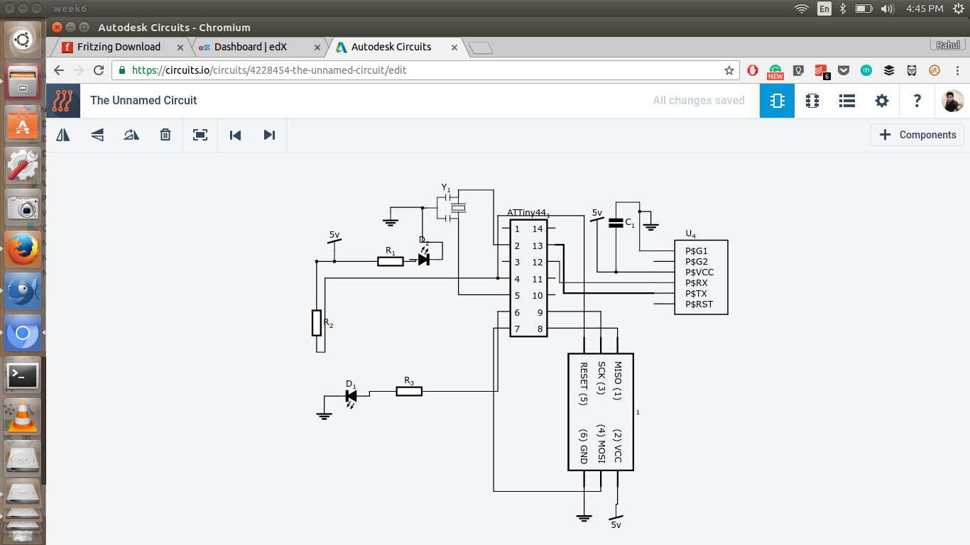
After inserting the components, just click on the two ends of the component and they will automatically be connected.You can switch over to the PCB view and rearrange the component use the Copper trace tool to draw traces between the components. There is no autoroute option, so everything should be done manually.
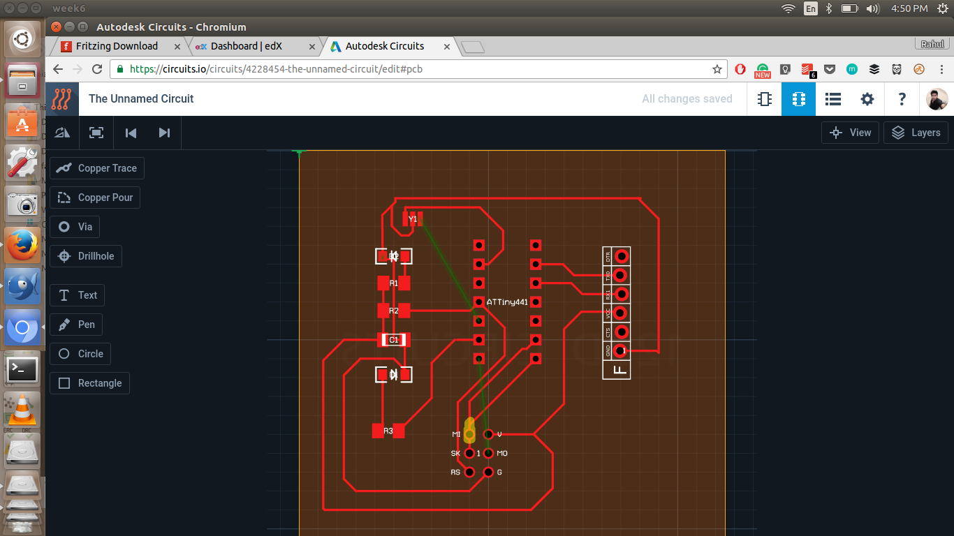
I liked autodesk circuits for its accessibility. I can switch over to windows and still work on my design, everything is saved in the cloud. Its good for designing simple circuits which don't have too many components. In board view autodesk circuits frequently went unresponsive, when I try to rotate and move components, might be the graphical load.
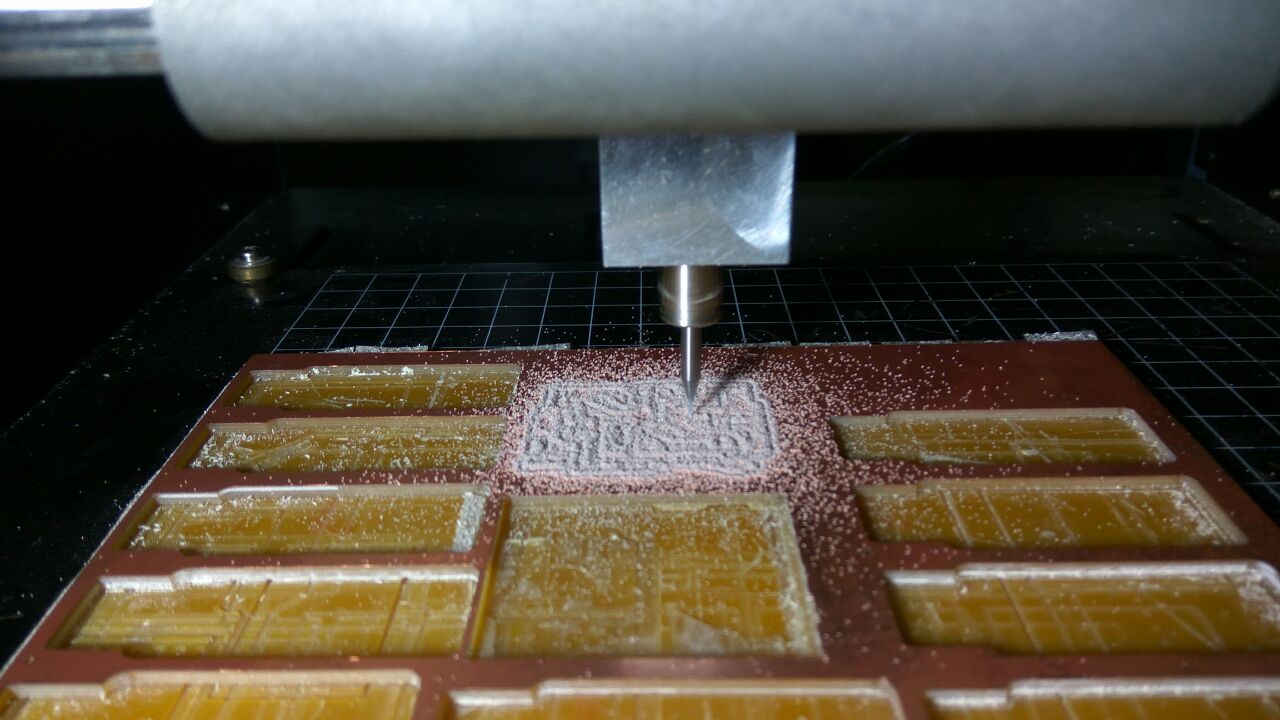
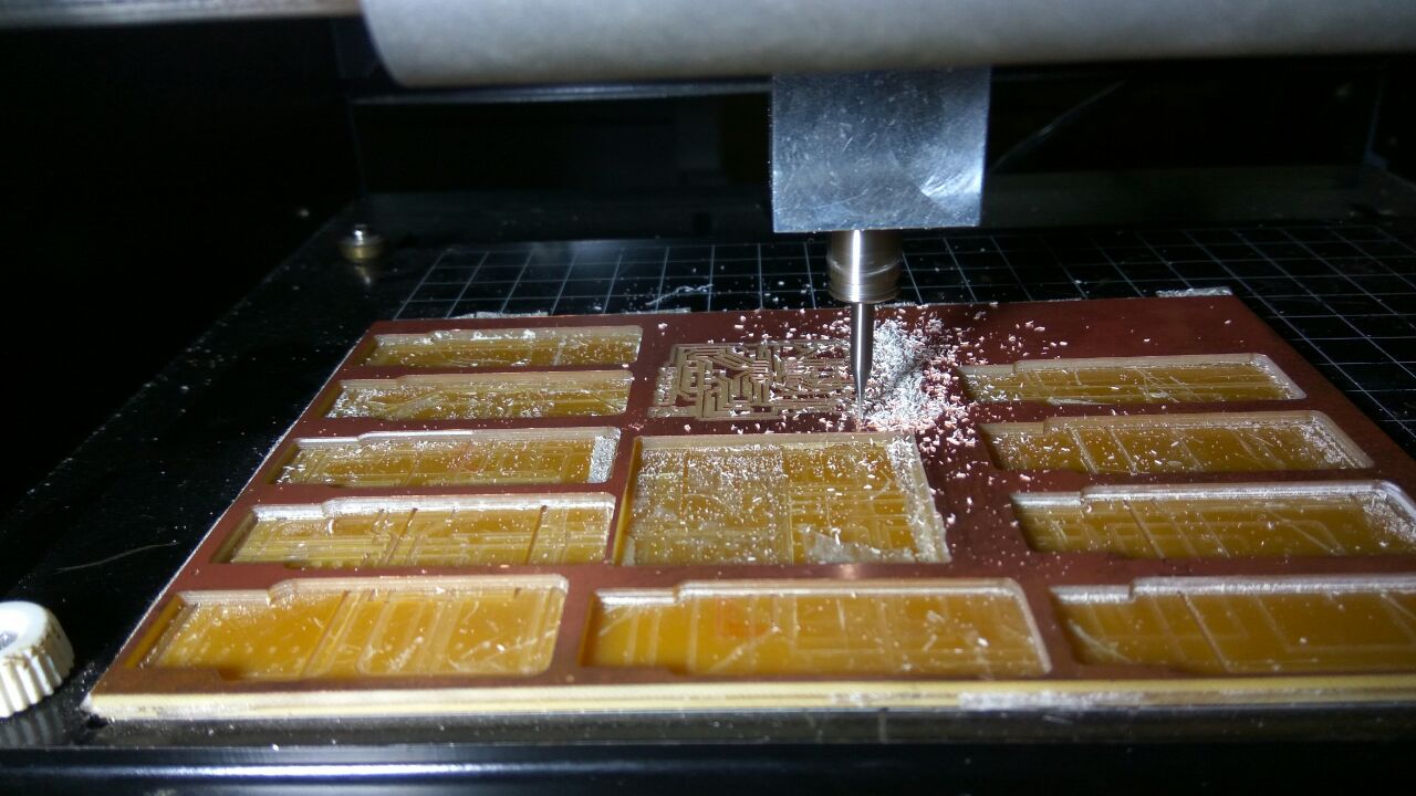
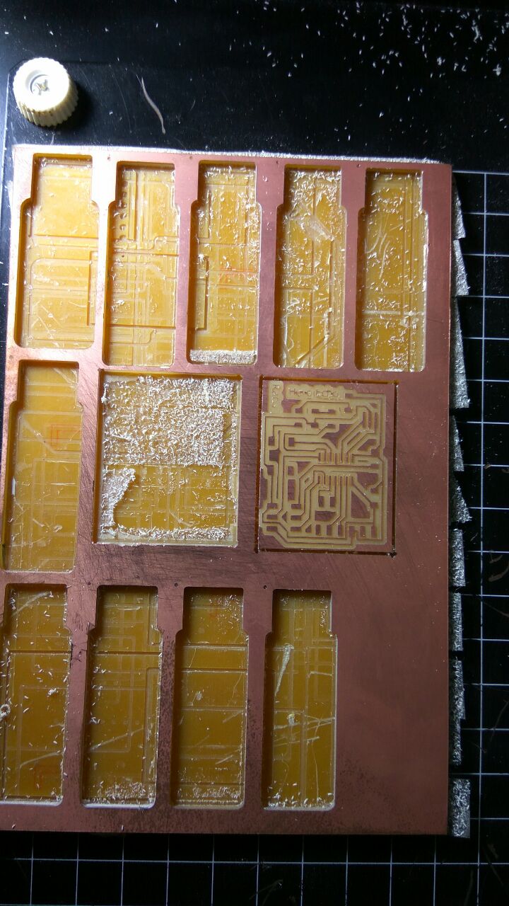
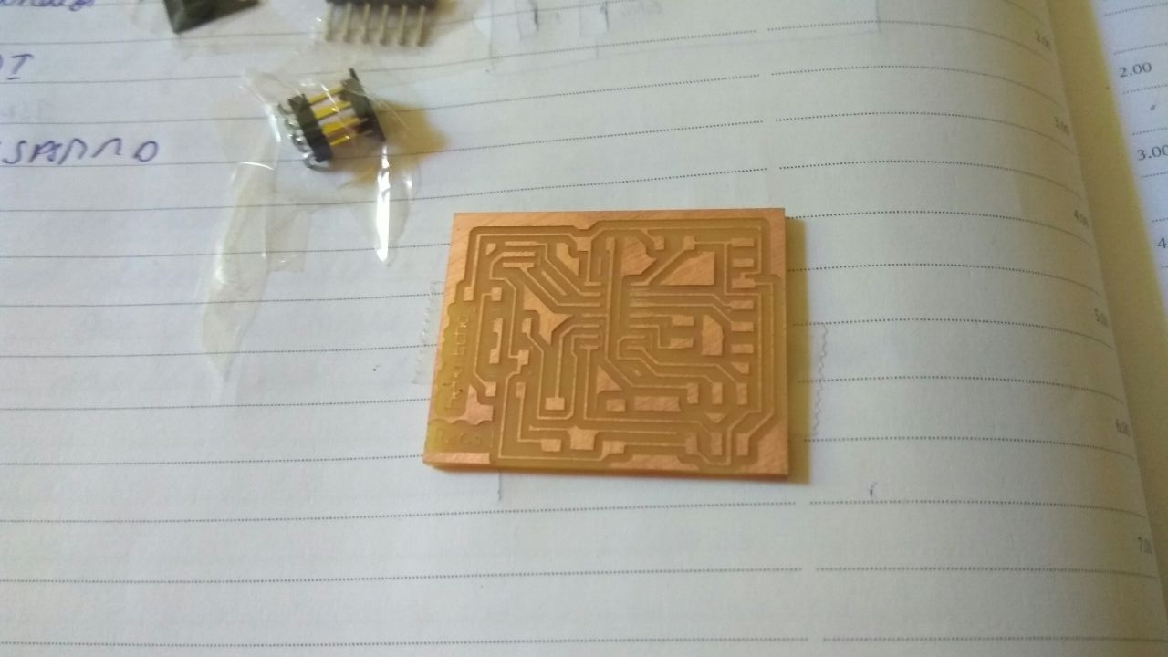
We use the Modella MDX 20 CNC mill to mill the PCB blank. The Details of which are covered in the week 4. I exported the board as a .png image and used the Fab modules to cut out eh board.

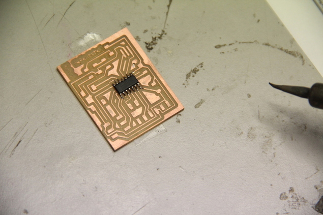
The next step is to stuff the board with all the components I will be following the same procedure as in week 4 to solder the components to the board.
Components Required
Made sure that the orientation is correct and the pins are properly placed on the pad.

I bend the Headers so that they would be perpendicular to the board.
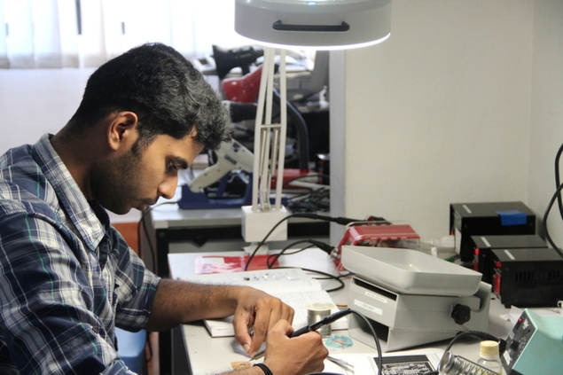

Now that I have some practice soldering the components, I was able to do it much faster than before. But soldering the Resonator was hard as it completely covered the pads, Hence I had to put it slights to one side, solder one pad and then finished soldering the rest of the pads and came back to solder the first pad.
Note: When soldering the Switch, you must orient it properly. The switch is symmetric and it is difficult to know which points are internally connected. An easy solution is to use a multimeter to check the continuity between the leads so that you can orient it properly. You should also consider this when designing the schematic of your board.
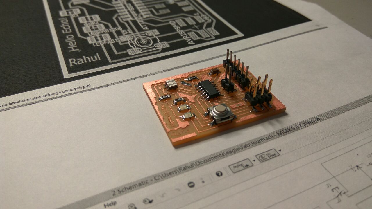
I had added two extra pads to the two empty pins on the board so that I could connect them to a header pin and use them as I/O pins. I cut out the traces and the pads were fine and I was able to attach the header to the pads.

But unfortunately while handling the board during programming, I had accidentally ripped off the traces of the pads. Now there are no pads left to solder them back to.
In my efforts to fix the board, I first thought to cut small pieces of copper sheet and stick them to the pad and solder the headers back on. But this proved unfruitful and I had an other idea which I thought was good at that time. I thought if I could drill two holes on the board, I could stick the header pins in solder the joints. This turned out to be a bad Idea as the solder does not stick well to the board and the traces to the pads are too far removed.

As you can see, it did not work and I'm left with two holes on my board.Lesson learned. Always treat your board with care.
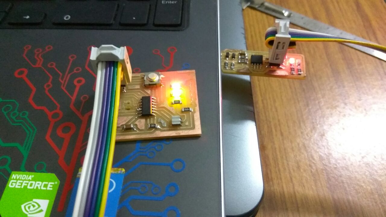
I wanted to see if my board was working, hence I decided to flash Neil's Hello echo program on my board. I connect my board with my ISP programmer I made in Electronics Production week, and proceeded to program the board. Since I added an LED between VCC and GND, It lit up and I knew the board was working.

Note: When connect the ISP header always refer your schematic and connect the corresponding MISO, MOSI, VCC, and GND pins.
I downloaded the make file for the hello echo board from the archives and proceeded to flash the board.
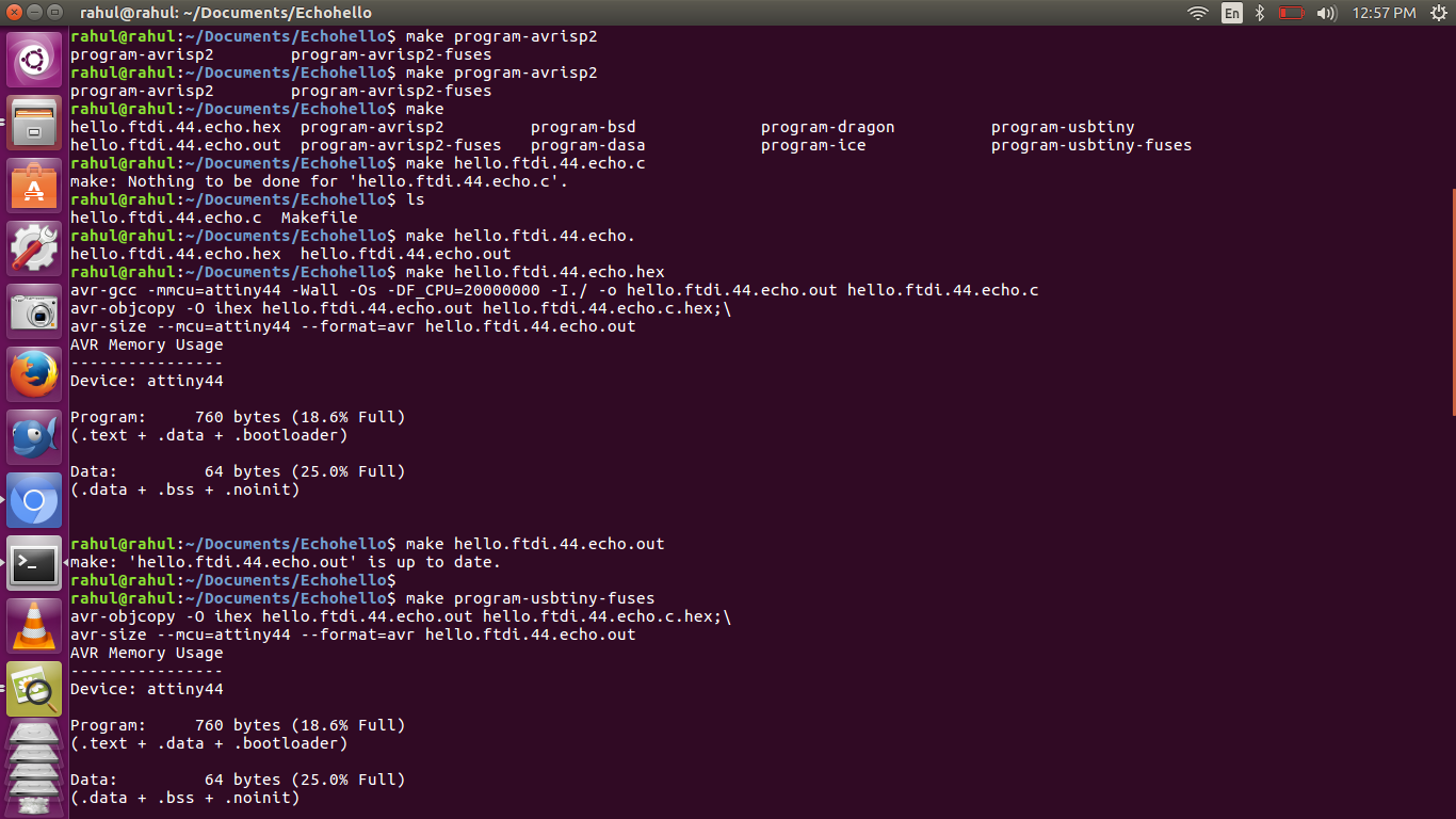
Using avrdude to make the Hex file
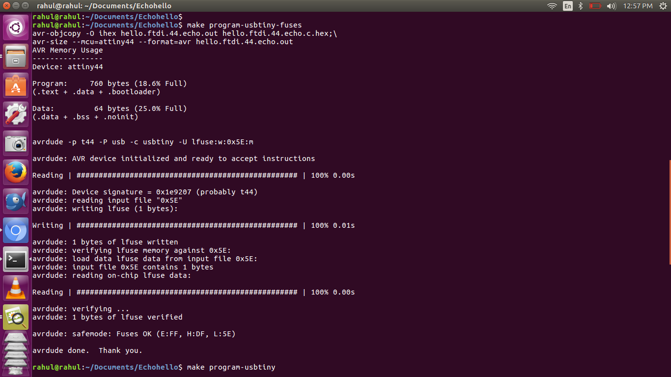
Since we connected an external 20MHZ resonator to the ATtiny, we have to set the fuse to use the 20MHZ signal instead of the 8MHZ internal clock.


I got the usb to serial connector and plugged it into the FTDI header. Note: connect the usb cable properly by looking up the FTDI pin out and align it with the GND VCC pins of FTDI header.
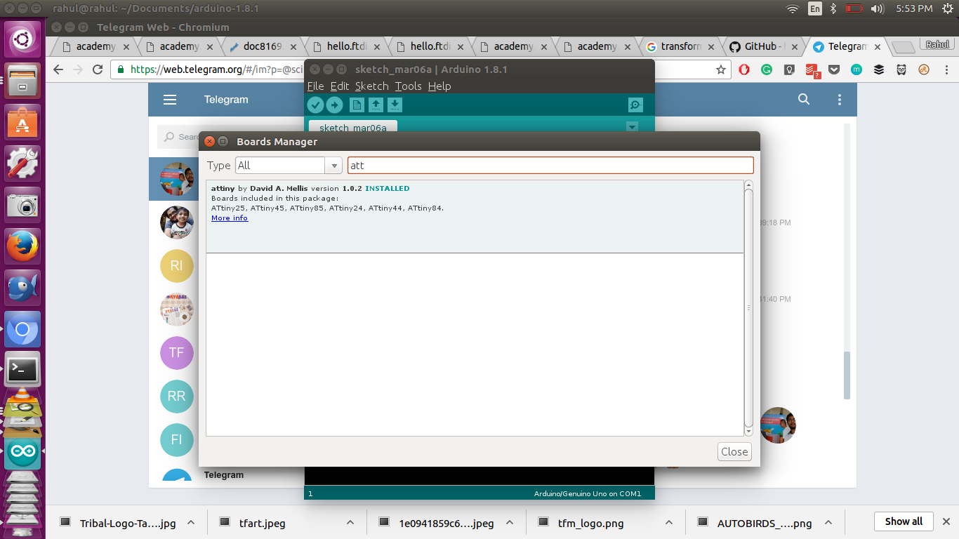
Installing the Attiny board to Arduino using the board manager.
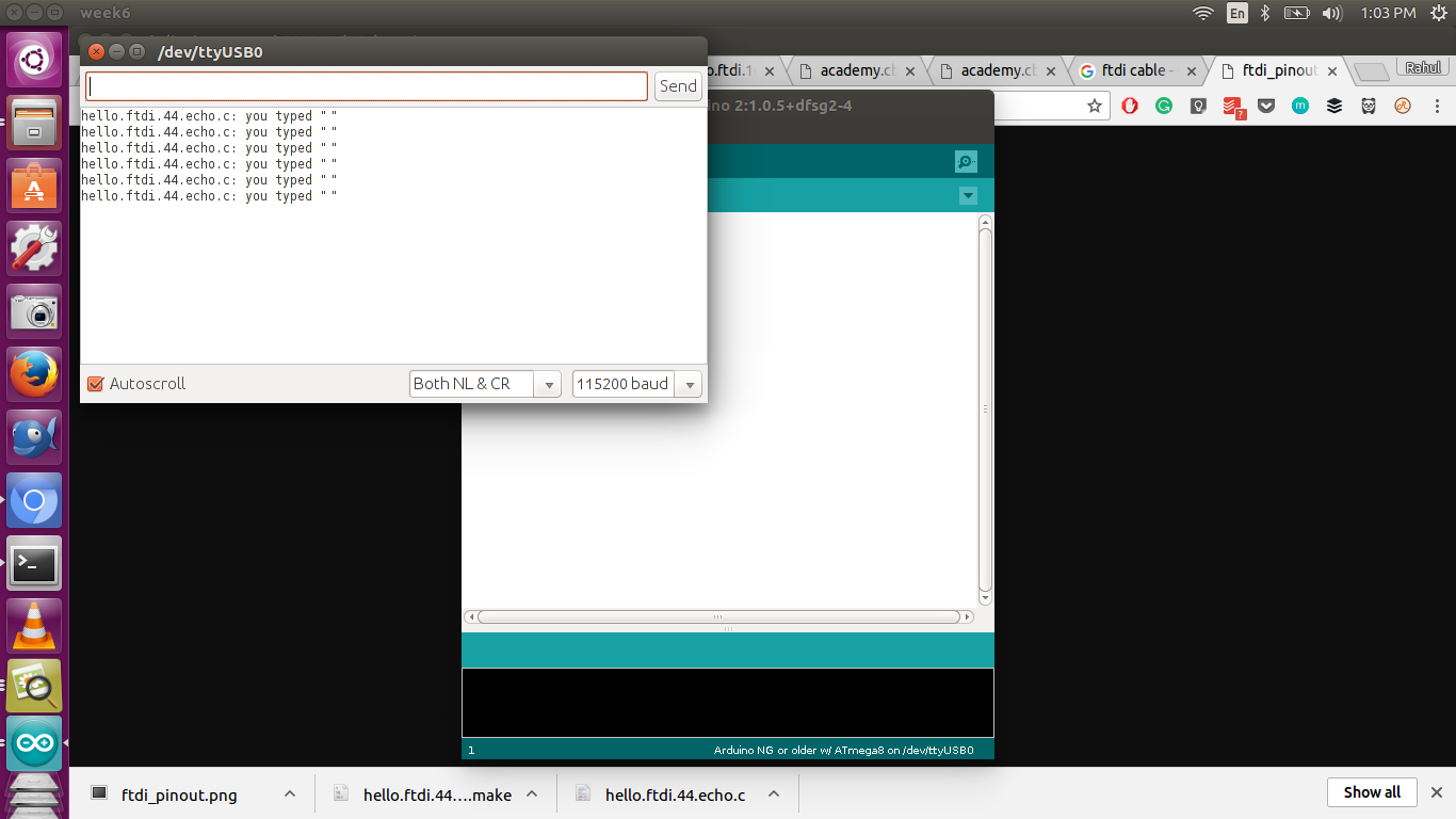
Trying to communicate with the board using arduino's serial monitor. It did not respond at first, we tried reinstalling the board in board manager, changed all the settings for programmer and the board, and finally we shut everything and restarted arduino and it was responding properly
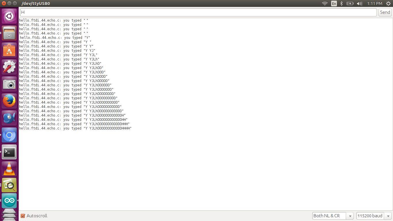
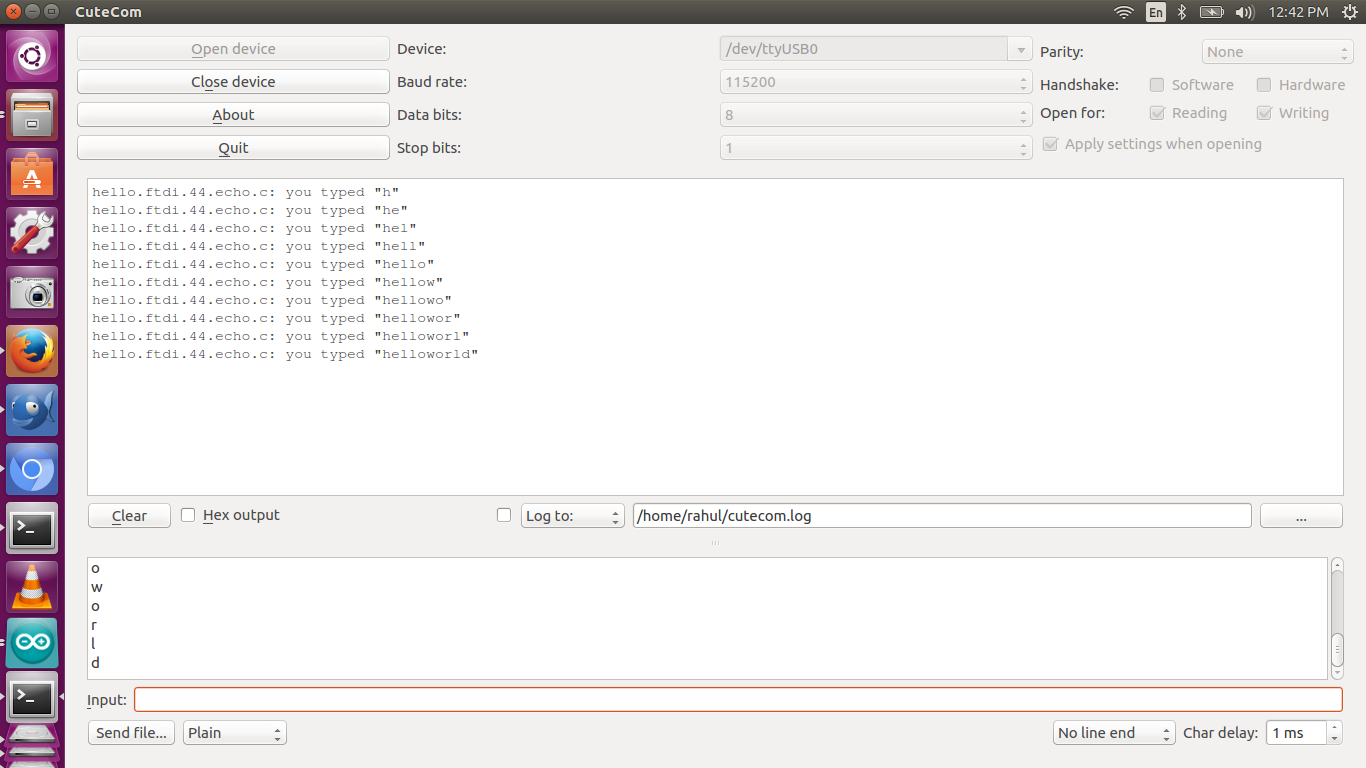
Our instructors told to install cutecom for serial communication It is working fine, and I'm able to get the output.
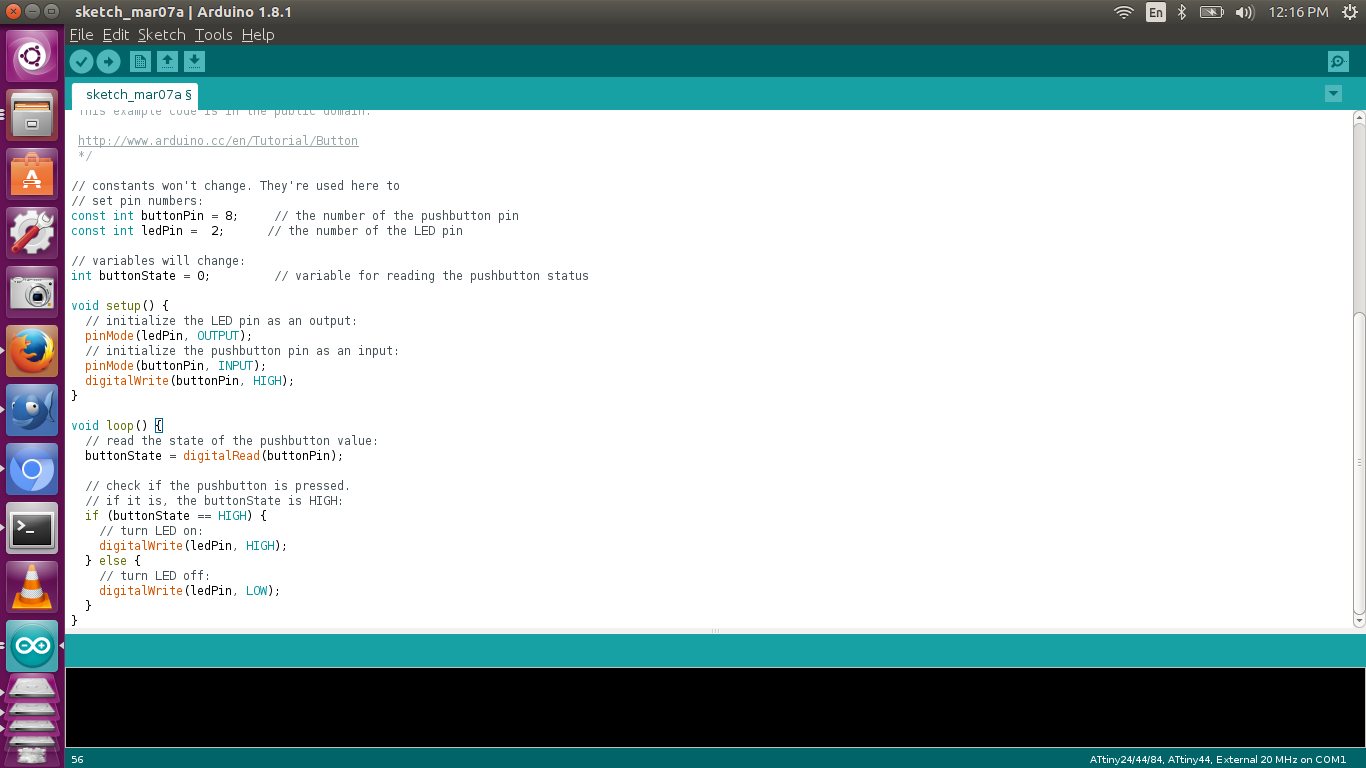
I used an arduino example program for turning on the LED when a button is pressed. I changed the pins of the program to correspond to the pins on my board after referring the Arduino pin datasheet of ATtiny. The program was flashed successfully after burning the Arduino bootloader. But it did not work properly the first time. We fixed the problem by adding digitalWrite(buttonPin, HIGH) This initialized the pin the button was connected to as HIGH and when the button was pressed it would become low. Now the code works and it was successfully lashed into the board.
The program works and now when I press the button the LED will turn OFF and ON.
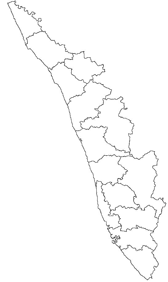
Originally I wanted to create a map outline and place LEDs where all the Fablabs are located, but since then I reduced it to a basic design of the map of Kerala and put two LEDs where the Fablabs are located. One in Trivandrum and other in Kochi. I searched online and found an outline image of Kerala showing all the districts. I then edited the file to remove unwanted parts. I opened the file in Paint and exported as Monochrome Bitmap Now I have to import this bit map into eagle.
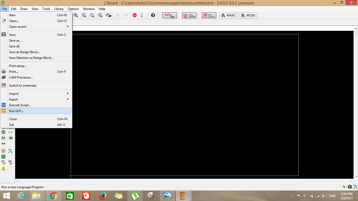
In board view go to File>Run ULP

Select import-bmp-ulp
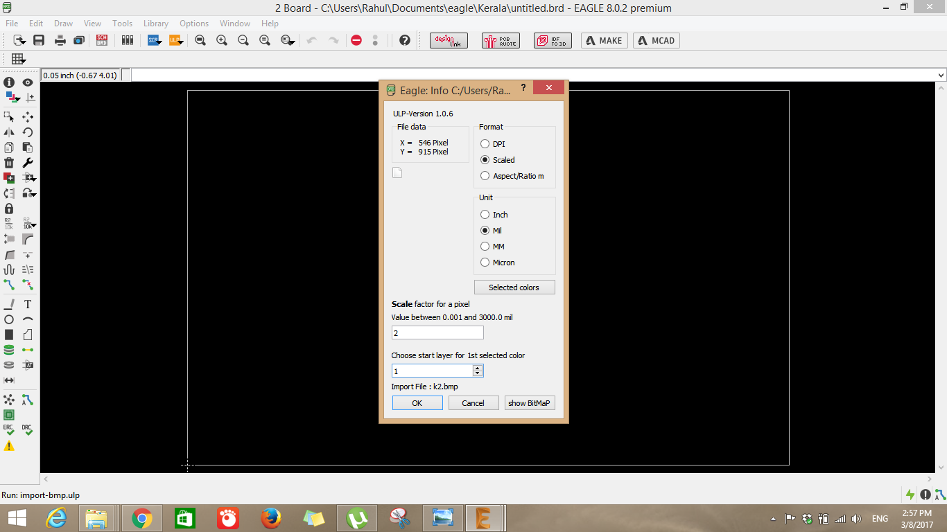
Try different scales to find the correct one

I designed a simple schematic which has two LEDs and a Resistor. The use of ICs are not needed as I'm not planing on programming the LEDs.
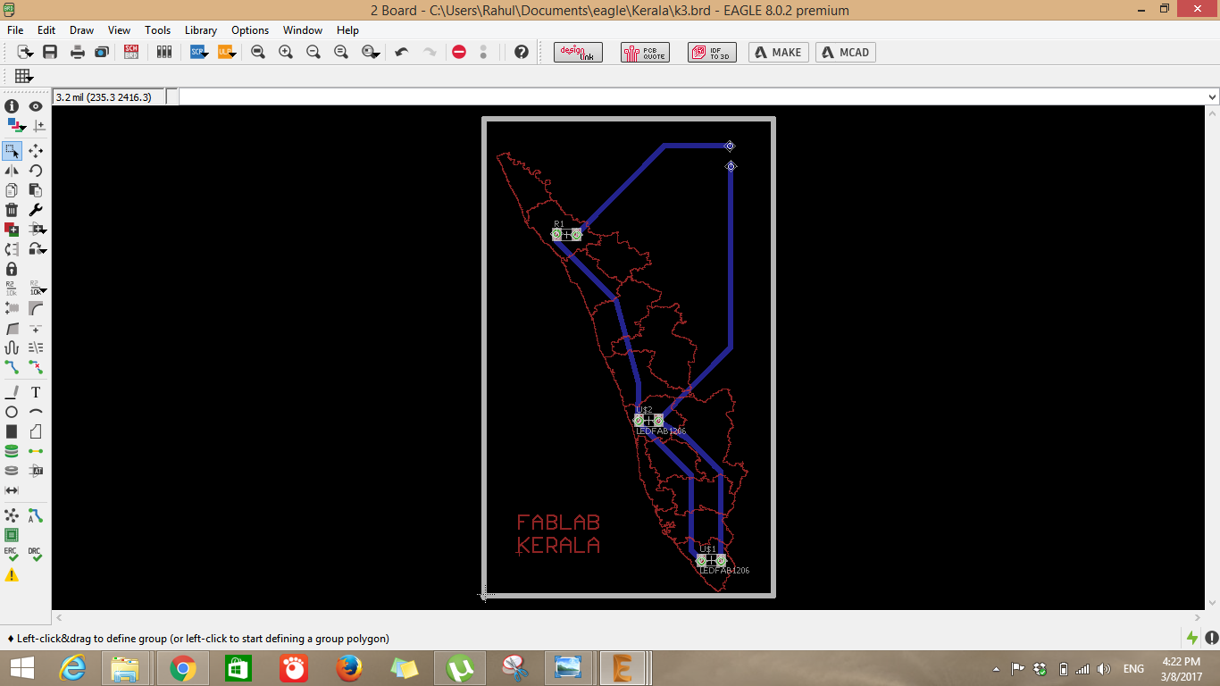
I wanted to make the face of the board look clean hence all the power connections will be given on the bottom layer. I plan on vinyl cutting the bottom layer and sticking it. I gave vias at all the points on the pad so that it can connect to the bottom of the pad.
Currently I did not have time to mill the board, but I learned a lot about importing bit maps into Eagle, I will try it in the future.
rahulsrajan.com
rahulsrajan01@gmail.com
Trivandrum, Kerala ,
India.

Technopark, Kerala, India

