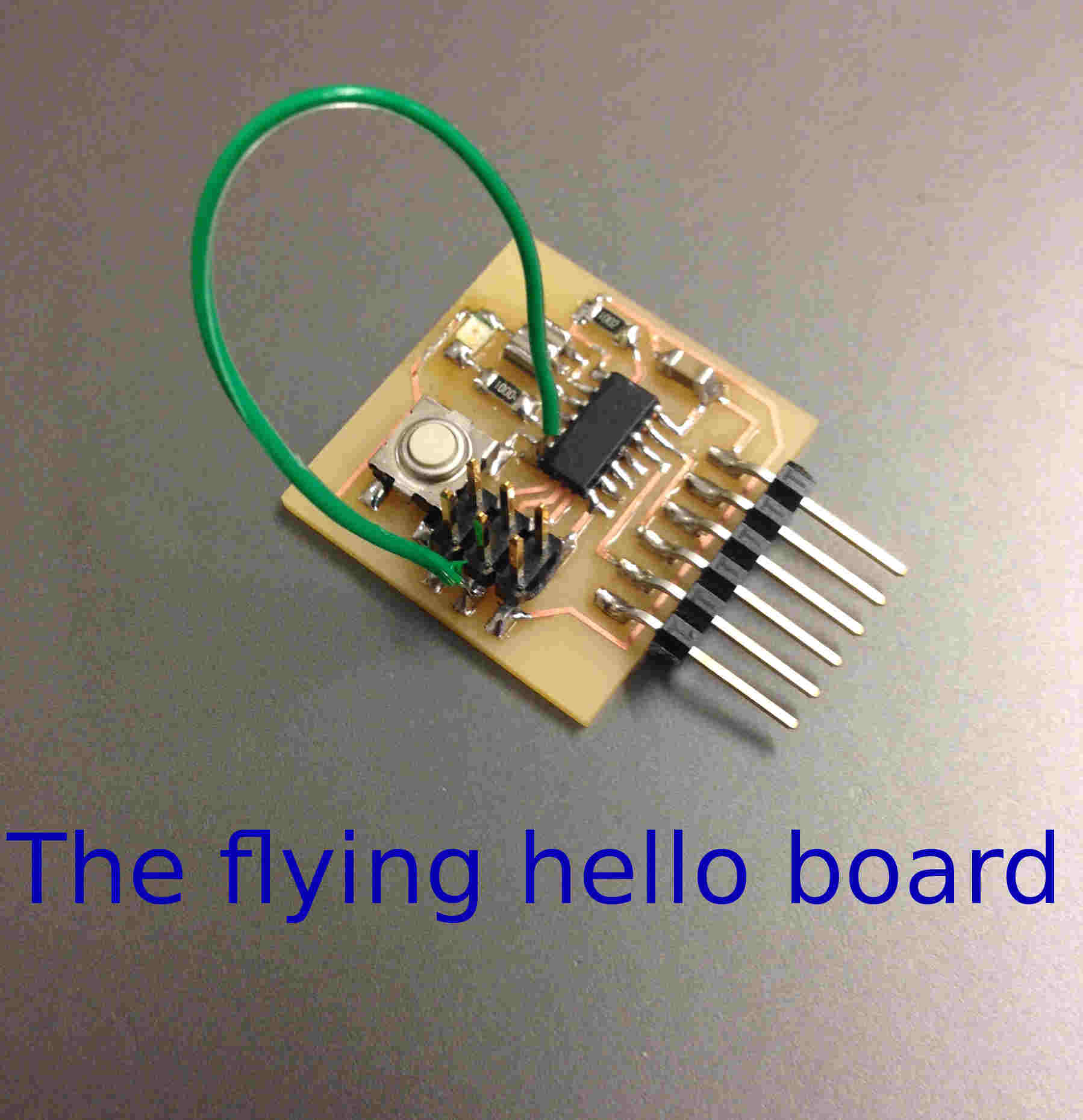
This week we we're asked to redraw the echo_hello-world board, add to it a LED and a button and, after checking design rules were respected, make it (mill it, solder it, check it work).
Prerequisites
I' ve been studying electronic at university for what regards Physic's electromagnetic
theories quite recently and continuously (Physic's course at Engineering, in Italy at
least, is a friend that usually goes along with you for more than a exam period) and
I admit I liked the subject quite a lot, despite I never had an occasion to see the
practical application of those laws.
Honestly, I realized what I knew wasn't enough to understand how to link a microcontroller
to a button or a LED but it helped me a lot in facing with some basic definitions, rules and
components name (in italics) you have to know when diving into electronic production:
- Ohm's laws:
- current;
- voltage;
- resistance (-->RESISTOR);
- Power (P= I2 x R );
- Anode and Catode;
- CAPACITOR;
- MICROCONTROLLER;
- Kirckhoff's laws:
I know there are loads for further words and definition to be clarified (also to me)
but I believe that if you already have a vague idea about definitions above, you can
start this weekly assignment without panic.
If you can't understand a single word of those I listed, DON'T PANIC as well!!
What I suggest you to do is to read chapter 2 and 3 (at least ) of
Practical Electronic for Inventors by Paul Scherz and also chapter 1, 2 and 4 of
Electronics for Dummies by Gordon Mc Comb and Earl Boysen - this book is a good starting point for those whose electronics knowledge is as big as a sand's grain.
EAGLE 7.7.0: import libraries and examples
1.How to import a library on EAGLE
I decided to start my week with the most common software for electronics design:EAGLE.
I already had it on my computer so I didn't have to download it.
Anyway I didn't know how to import an already-written library (and I needed to do it to get
fab.lbr to design my board),
so I had a look at
this tutorial.
Briefly, what you had to do is:
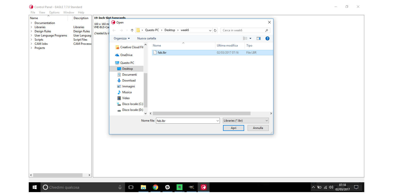
- 1-Open EAGLE and go through File-->Open..->Library and type .lbr file path:
- 2-Go trough File-->Save as.. in your library window's menu bar and save .lbr file in EAGLE-#.#.# \ lbr (# stands for software version number) :
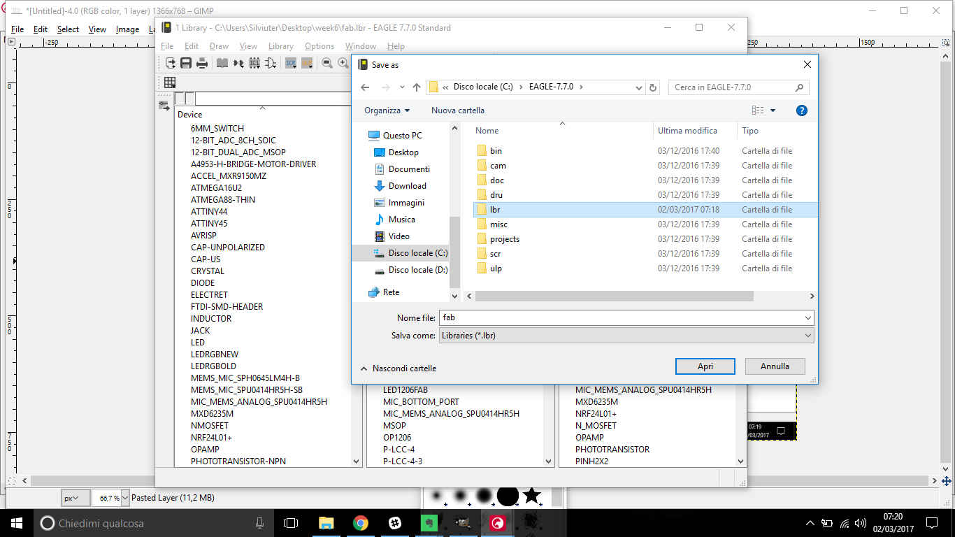
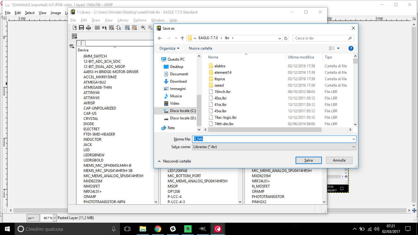
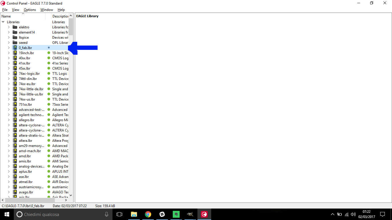
NB: I changed library name putting a "0" before so as to have my library on top the list, as shown below:
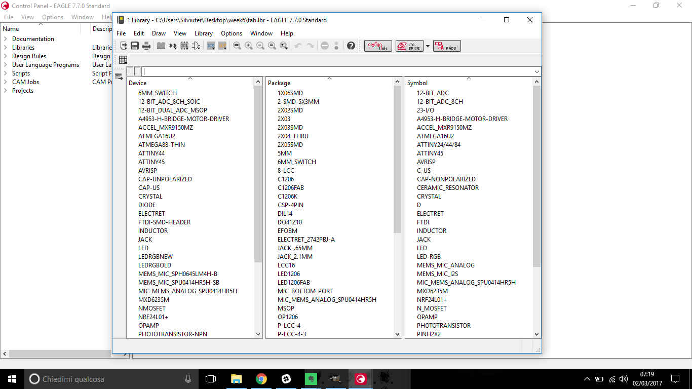
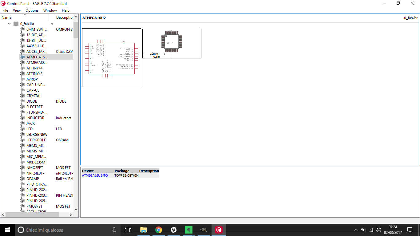
Going through the library, you can see details of each component just by clicking on it:
2.hello world board example
XMEGA version
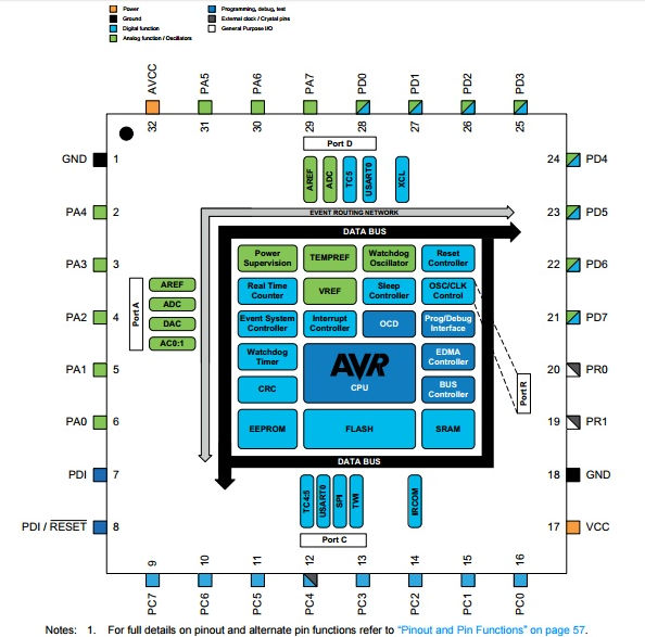
Making acquaintance with XMEGA 16e5
What I then wanted to do was to get to hello world board example and to make myself an idea about components and how they were linked.
I first glanced at two images I found on the week schedule: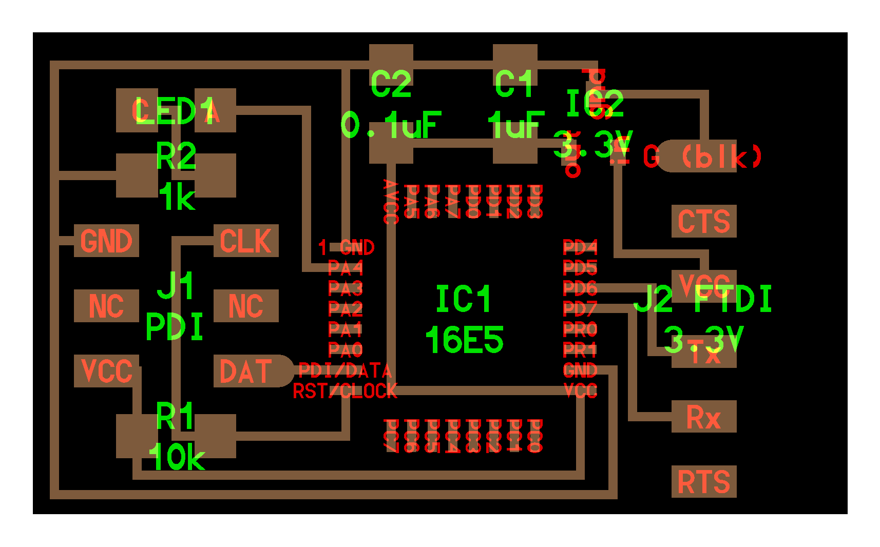
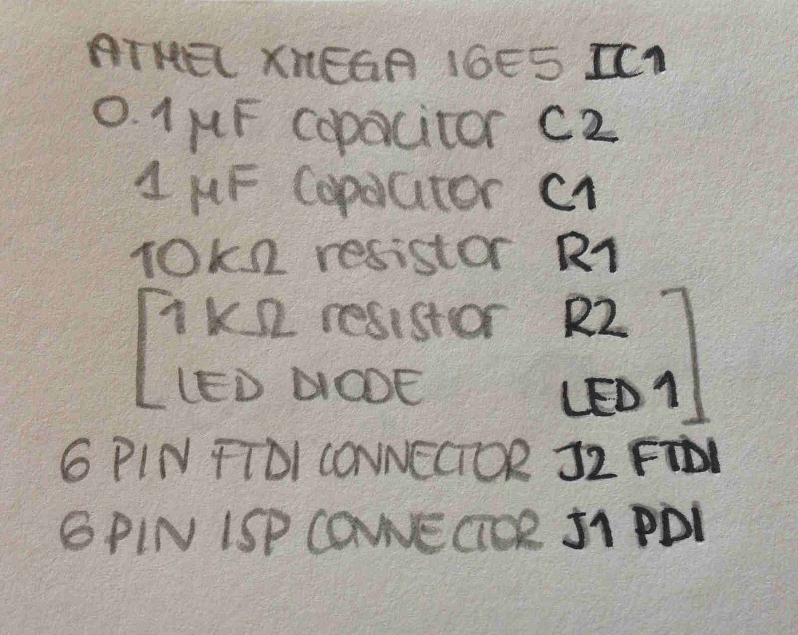
 I so tried to write down my BOM from the first picture:
 Analyzing the second one I tried to give each component its name:
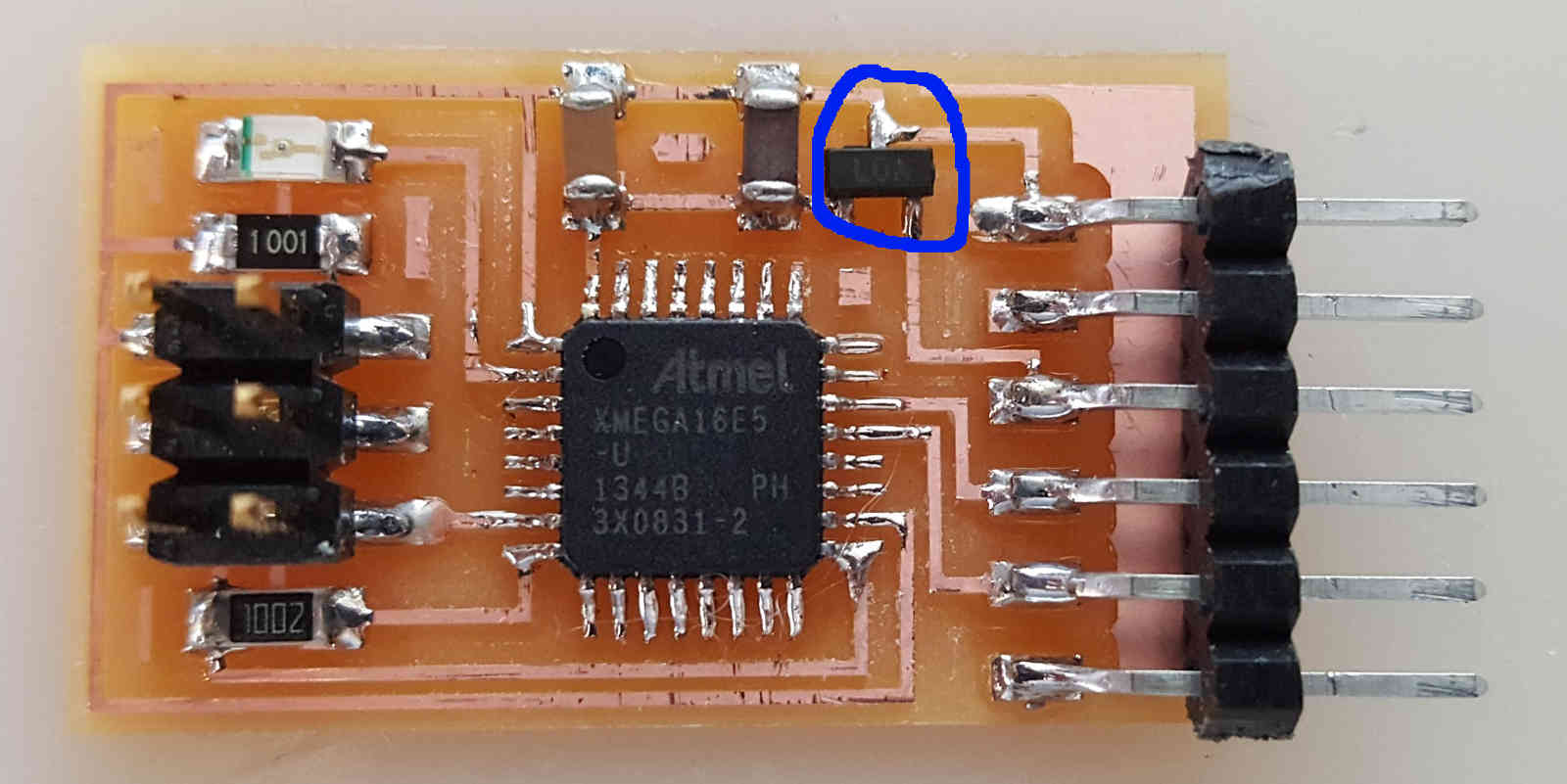
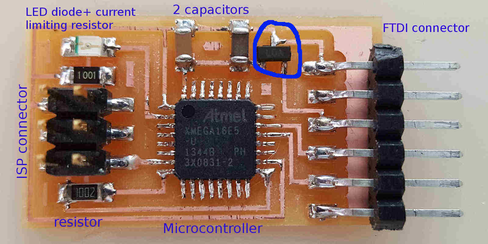 NB: that 3-pin something I circled in blue was missing my mind.
I then wanted to get to board schematic 1 and I so opened this tutorial from Fab Academy archive, hoping to find the file I was looking for but unfortunately I received a "404 Not Found" after clicking on this link at step #2.
Therefore, I moved to last year documentation written by my instructor and, since I'm dumb I just downloaded schematic file and opened it on Eagle. I immediately found some incongruities:
- I still didn't find what that 3-pin component was (it couldn't be a resonator);
- I was missing 0.1μF capacitor;
- microcontroller seemed to be different from the one I was supposed to use;
After...
- thinking my instructor made a mistake;
- feeling inner pain for pride sin;
- getting a confirmation about Atmel XMEGA to do be a microcontroller here and here ;
- checking my instructor board .png file was the same with mine (and it was NOT)...
....I realized I've been too summary in looking just to one previous documentation and in switching from the version I wanted to do to the one my instructor made last year. So..
IMPORTANT! when searching on the Internet, check the features of the board you want to make and be careful to get the right files (.png files and schematic)!
After this error I felt like:.jpg) ...but my cat said he loved me anyway :) !
...but my cat said he loved me anyway :) !
As soon as I realised there were two versions of hello world board I decided to go along with the first I met, the one with XMEGA 16e5 microcontroller. Which are the differences?
- XMEGA is a class of more powerful microcontrollers...
- Therefore they present little more difficulties in programming;
- Using this kind of microcontroller in making an hello world board gives you th opportunity to implement it more than with a LED and a button because you have a lot more of free pins;
- there are two capacitors instead of one (see BOM above);
- it already a LED and a resonator in series: baby there's no need to wise up, you still have to add one ;) ;
- it present a current regulator2 (yeah, that 3-pin something);
How to make a new device on EAGLE
It then comes to EAGLE design.
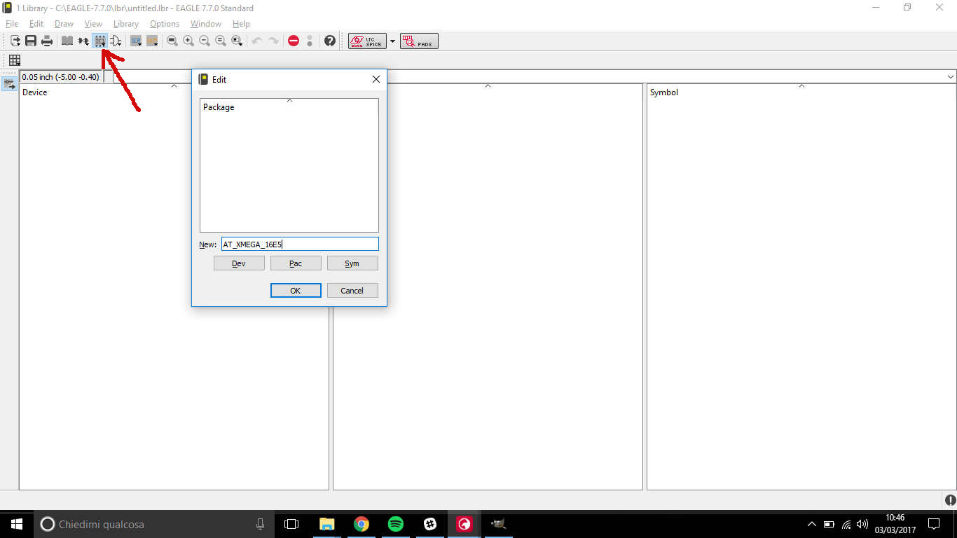
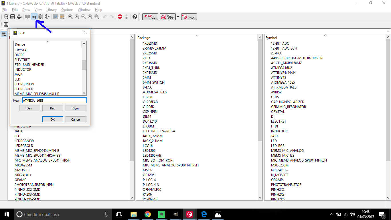
Owing to the fact that on fab.lbr there's no device3 for Atmel XMEGA 16e5
I had to create one. When you have to do that, basically you have to open your library and add a
package4 and a symbol5. In fact, each component on EAGLE is made of
this two elements, linked together: the package is your real component (so you have to check on
datasheet exact dimensions of pins, case etc) and pin function (to say it better, the name
related to pins' function) is said in the symbol.
Package design
I started drawing a package because I still didn't know there's a standard one on
fab.lbr that also suits Atmel XMEGA 16e5 features, but I learned that
from the datasheet (I'll tell you where in picture below) soon so I stopped wasting
time and patience in this precise but entertaining procedure.
 I will briefly explain how I started, getting lots of help from these tutorials and websites:
- on Adafruit.it there are great tutorials about both symbol and package editors;
- in this article there's a global overview about components design;
- PACKAGE:
- SYMBOL:
So, as I said, I started designing my XMEGA 16e5 package and I found this
part very challenging, because you have to be careful in respecting your components
dimension so as to have a realistic idea of size proportion among other board
elements so that you draw a schematic most like the board you'll mill.
IMPORTANT!: find and analyze dimensions info on
component's datasheet before drawing!!!
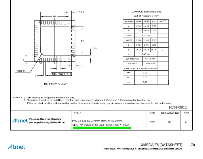
I found this technical drawings at page 68 of XMEGA 16e5 datasheet (PDF at the end of the page):
....Did you see those tiny words in the bottom of the picture?? Yes, dude,
I didn't care about them at first just like you, but they matter quite a lot...
Go back and read them, they'll be relevant in few steps
So, finally, we come to package design:
I went through File-->New..->Library to create a new library - this step isn't
necessary, if you feel confident not to make a mess into fab.lbr you can just open it.
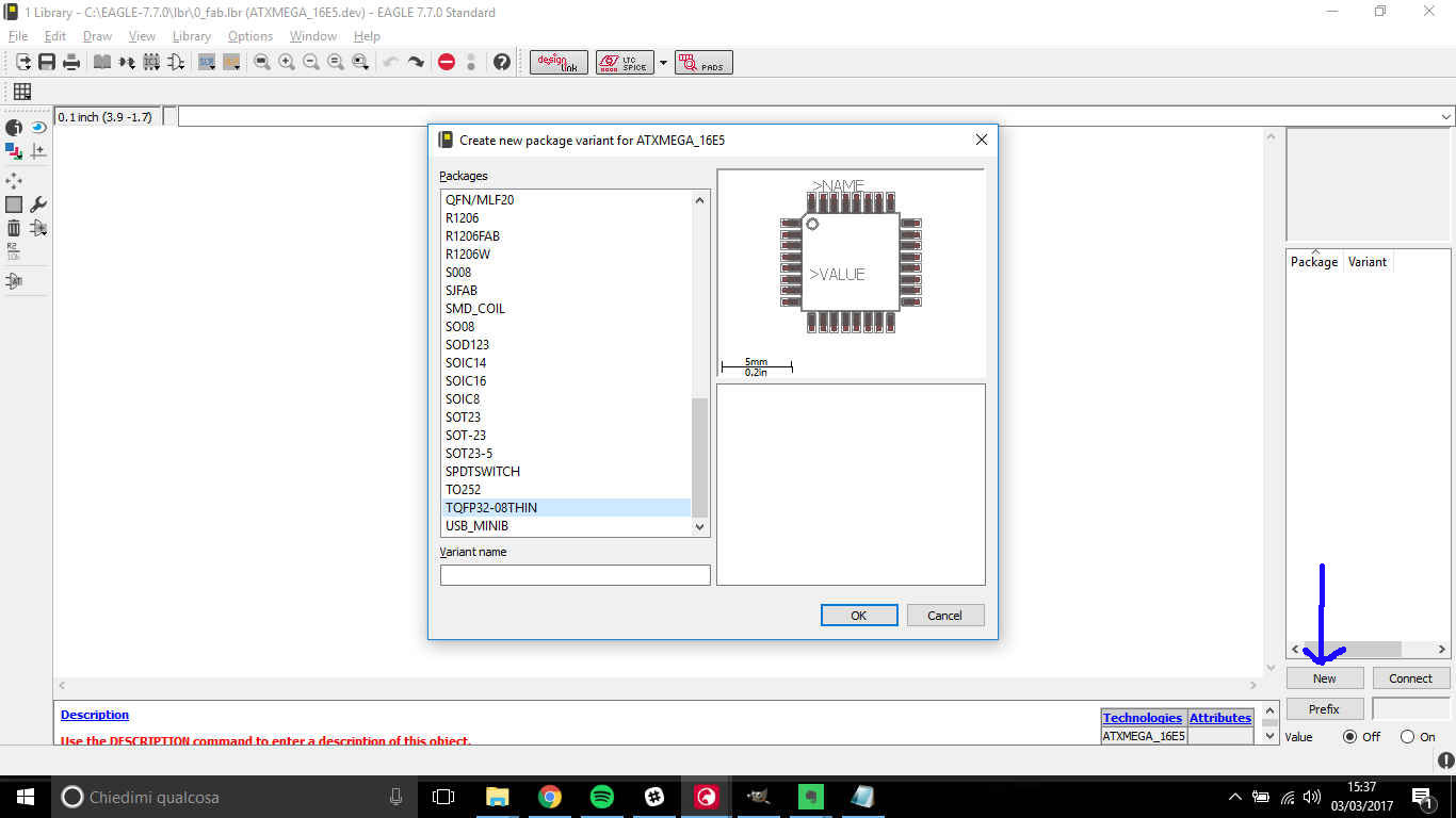
 I thenk clicked on Package symbol and create a new one
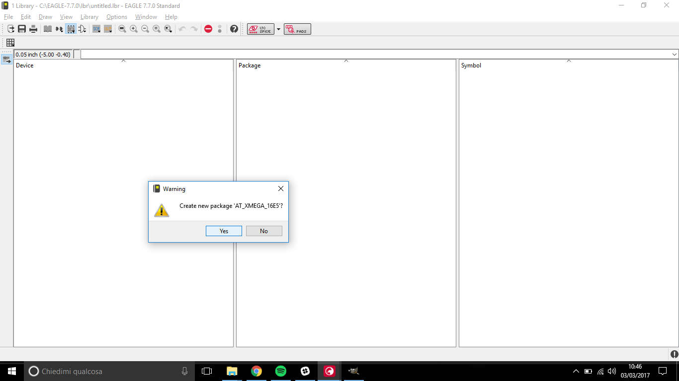
 After this operation (also for symbol editor) you will be asked to confirm your operation, click "Yes":
 The workspace becomes black with a grid:
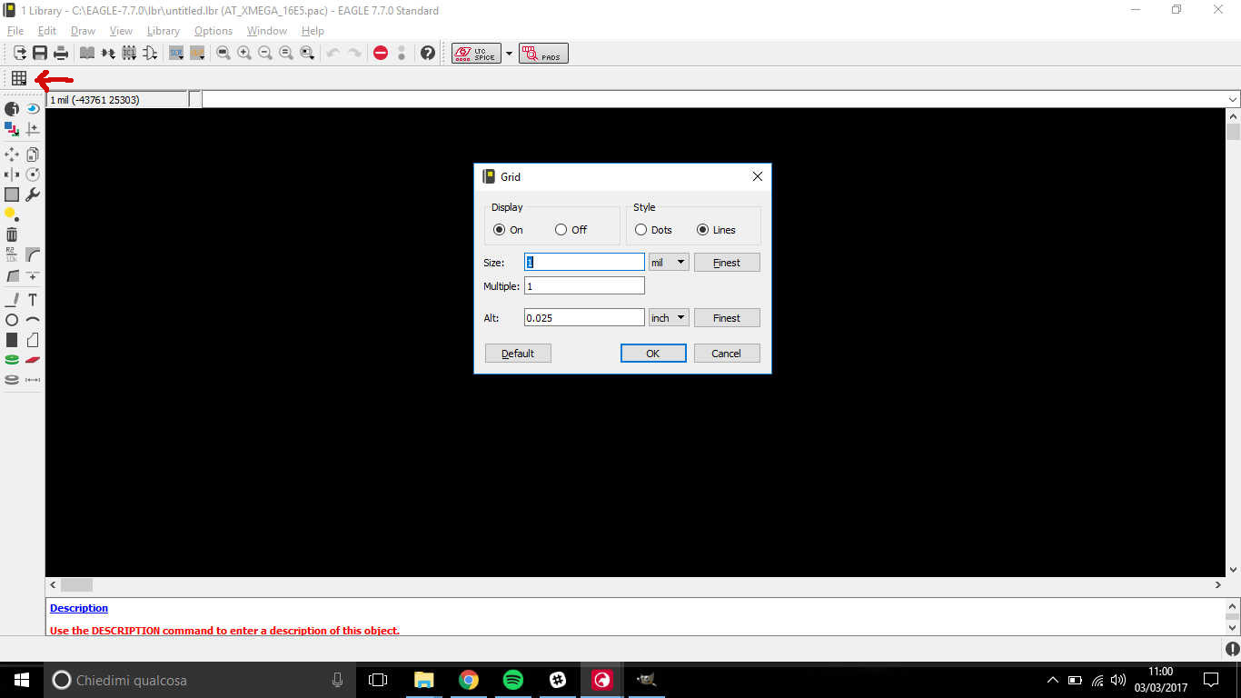
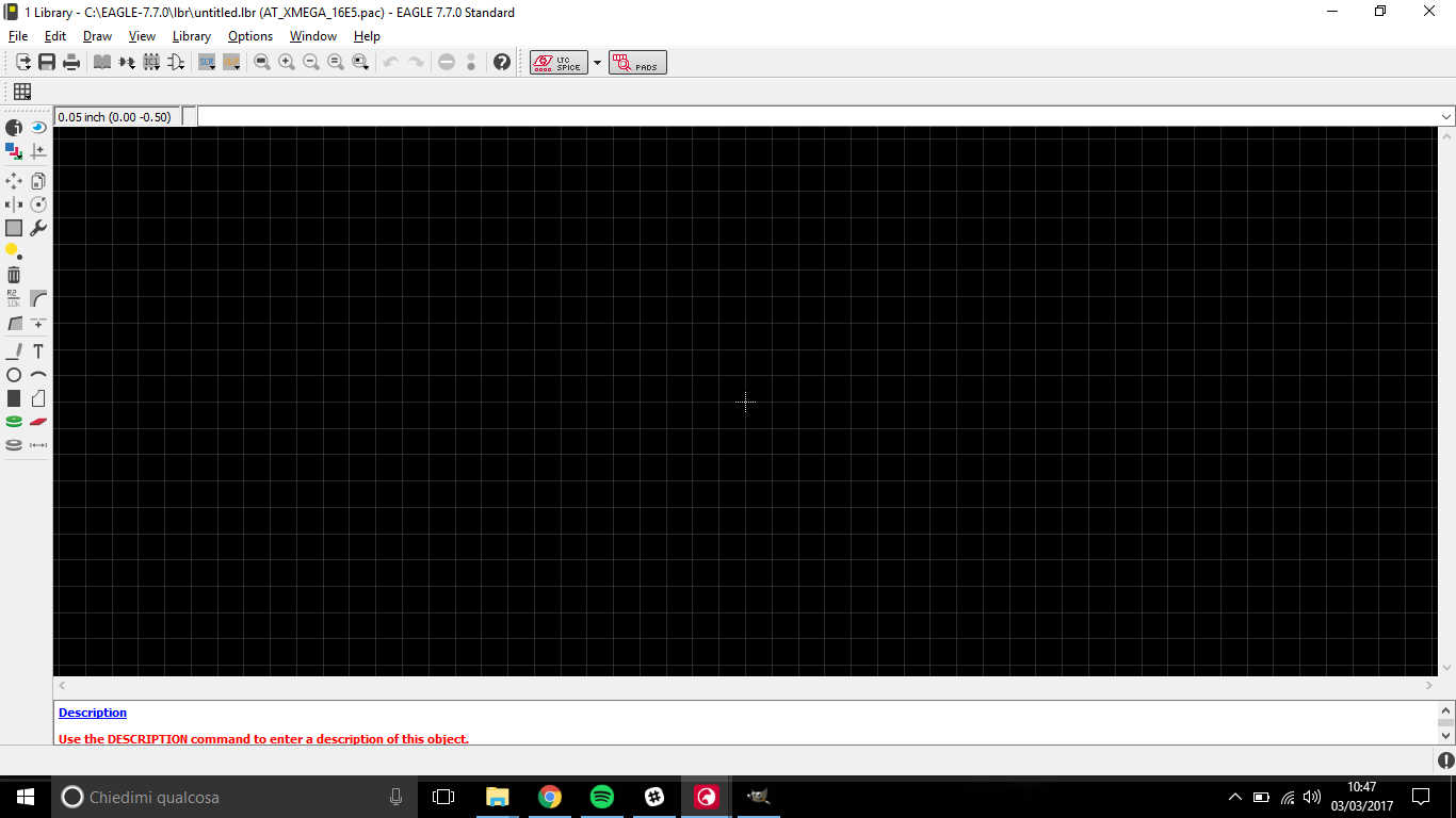 You can change grid features clicking on its symbol in the upper left part of workspace- I chose 1mm size:
 I then used WIRE
command in the command line above workspace:
I then used WIRE
command in the command line above workspace:
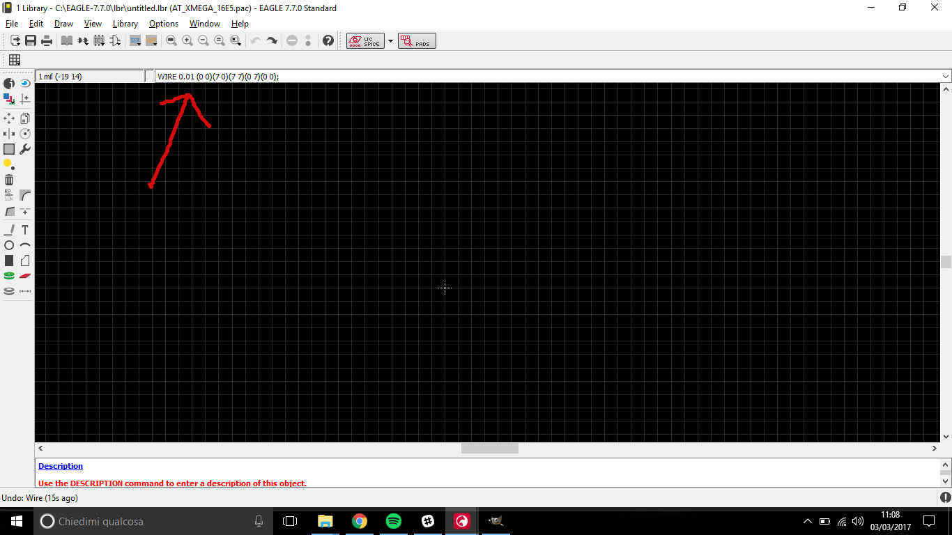 As you can see, the formula looks like WIRE #
(x0 y0)(x1 y1)(...) -where #
stands for line thickness- and in XMEGA 16e5 case I used 7mm side square.
As you can see, the formula looks like WIRE #
(x0 y0)(x1 y1)(...) -where #
stands for line thickness- and in XMEGA 16e5 case I used 7mm side square.
I then wanted to add pins to the microcontroller body so I clicked on
SMD symbol and changed size in upper bar to make them suitable to my
component (see datasheet and this file for my sketch dimensions).
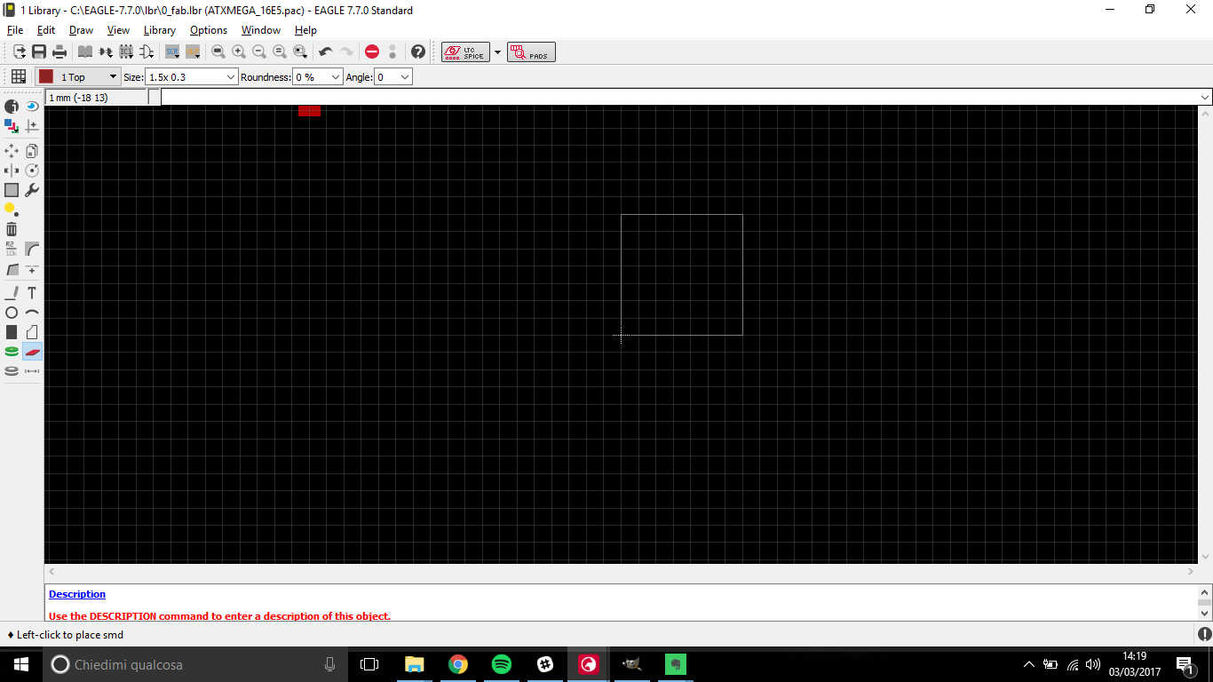 I then used SMD
command to put pads in (that one I think was) the right position:
I then used SMD
command to put pads in (that one I think was) the right position:
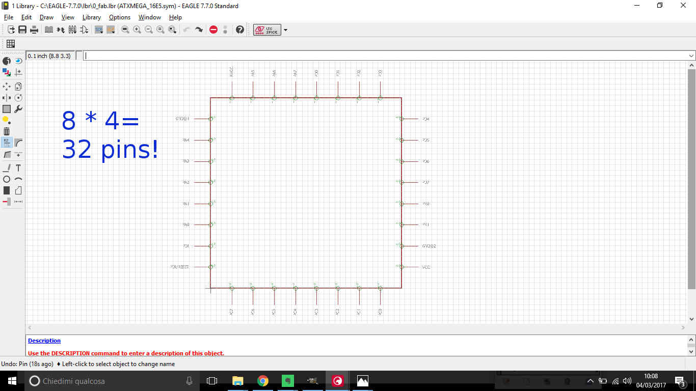
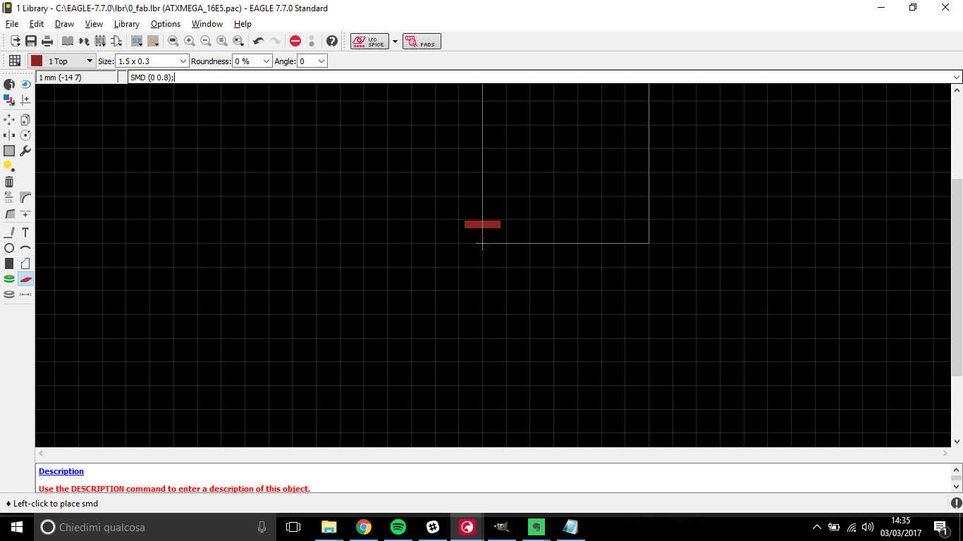 After putting 8 of them in the left side, I saw there was an error:
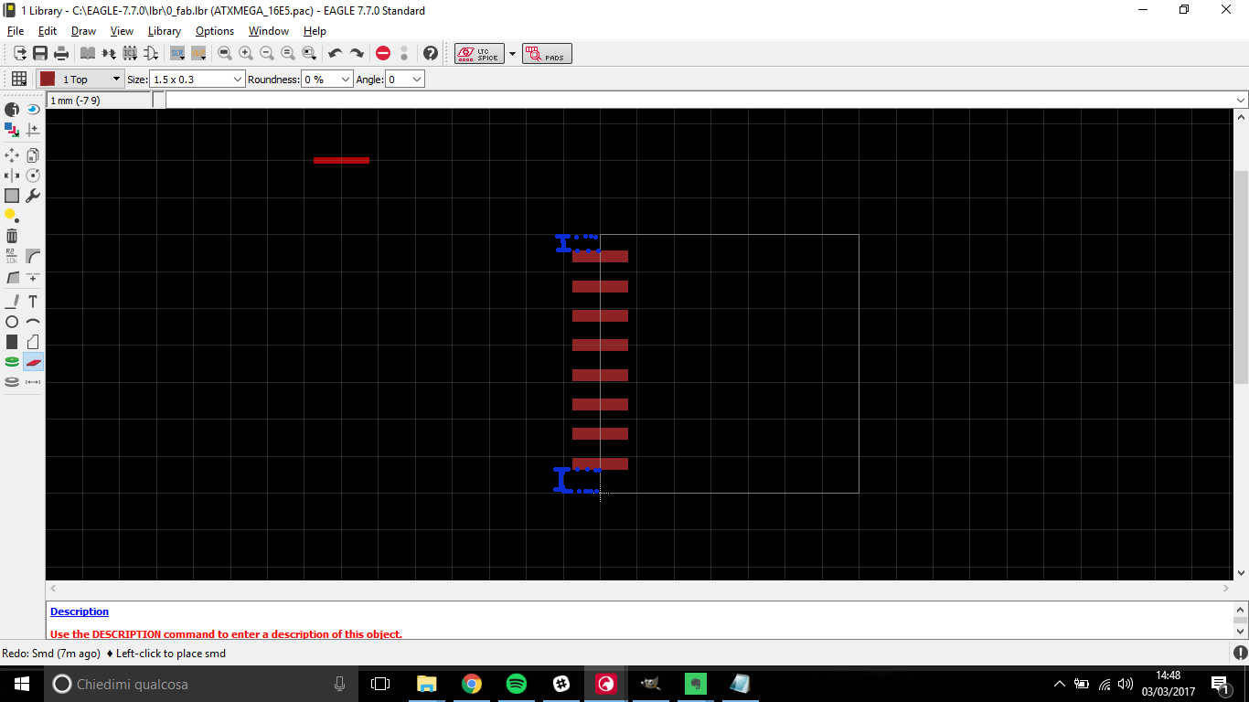 As you can see the upper first and last pin were shifted from edges with different quantities.
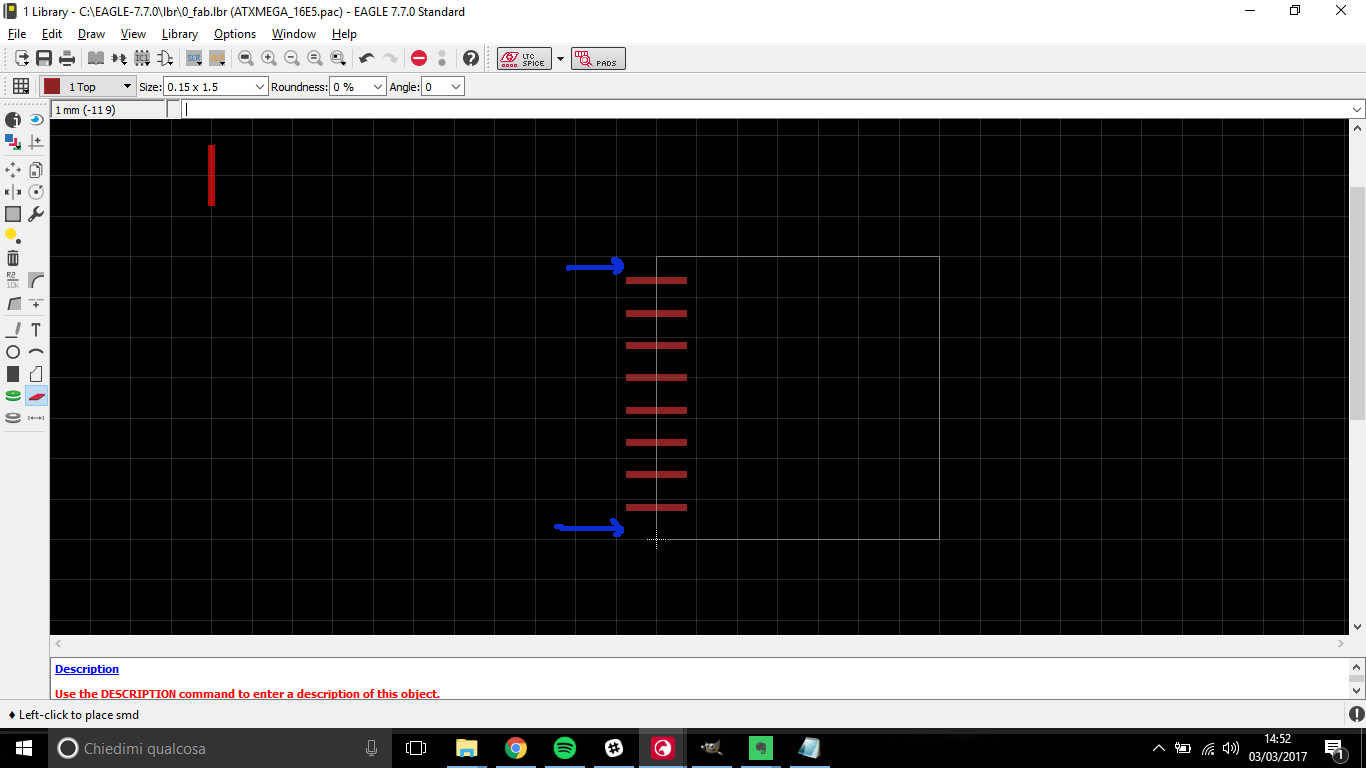
I tried to repeat the same procedure two times and the third with half thickness of SMD
but I still had same problems:
As you can see the upper first and last pin were shifted from edges with different quantities.
I tried to repeat the same procedure two times and the third with half thickness of SMD
but I still had same problems:
 I so started thinking there wasn't a reasonable reason why, to do this weekly assignment
all the students should have improved fab.lbrwith more than 200
almost equal packages of XMEGA 16e5.
I so started thinking there wasn't a reasonable reason why, to do this weekly assignment
all the students should have improved fab.lbrwith more than 200
almost equal packages of XMEGA 16e5.
....Meditating...
Do you remember I said those tiny sentences matter quite a lot?
That's because there's a sentence saying :
"This drawing is for general information only".
It made me think I was using dimensions (the ones in the table) that beside being discretionary
(there's a minimum, nominal and maximum value you can use) didn't even correspond to real
one. I searched for the document said to refer to but after five minutes of no results,
it came to my mind that it was impossible that loads of programmers haven't never found
a common design for XMEGA 16e5 device on EAGLE: so, after careful reading
of datasheet (just parts close to drawings, to be honest, because 300 heavy pages were
too much to be taken into consideration in just an afternoon) and I read that:
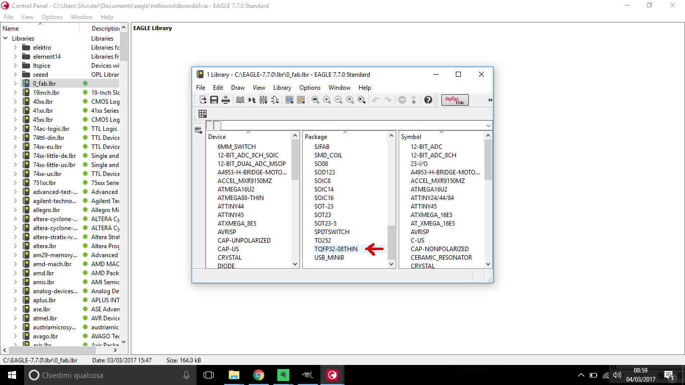
What the evil those words meant? they're package format acronym of XMEGA 16e5
and you can also find it on fab library:
 NB: please note that this package seems to have too large pads and, while milling, they really come out too close together; it will be enough to edit .png file of traces exported from EAGLE before sending it to fab modules
The problem in the line above, made me think I would really like to design a suitable package
for XMEGA 16e5 but it really takes a lot to do it precisely, so I preferred to follow
.png editing way.
Symbol design
Since I had the package of XMEGA 16e5 but not its symbol, I created a new one clicking on Symbol button:
 To make my symbol, I just used these commands:
- Wire;
- Pin;
- Name;
Result:
 To give proper names to pin I referred to datasheet description:
 NB:
NB:
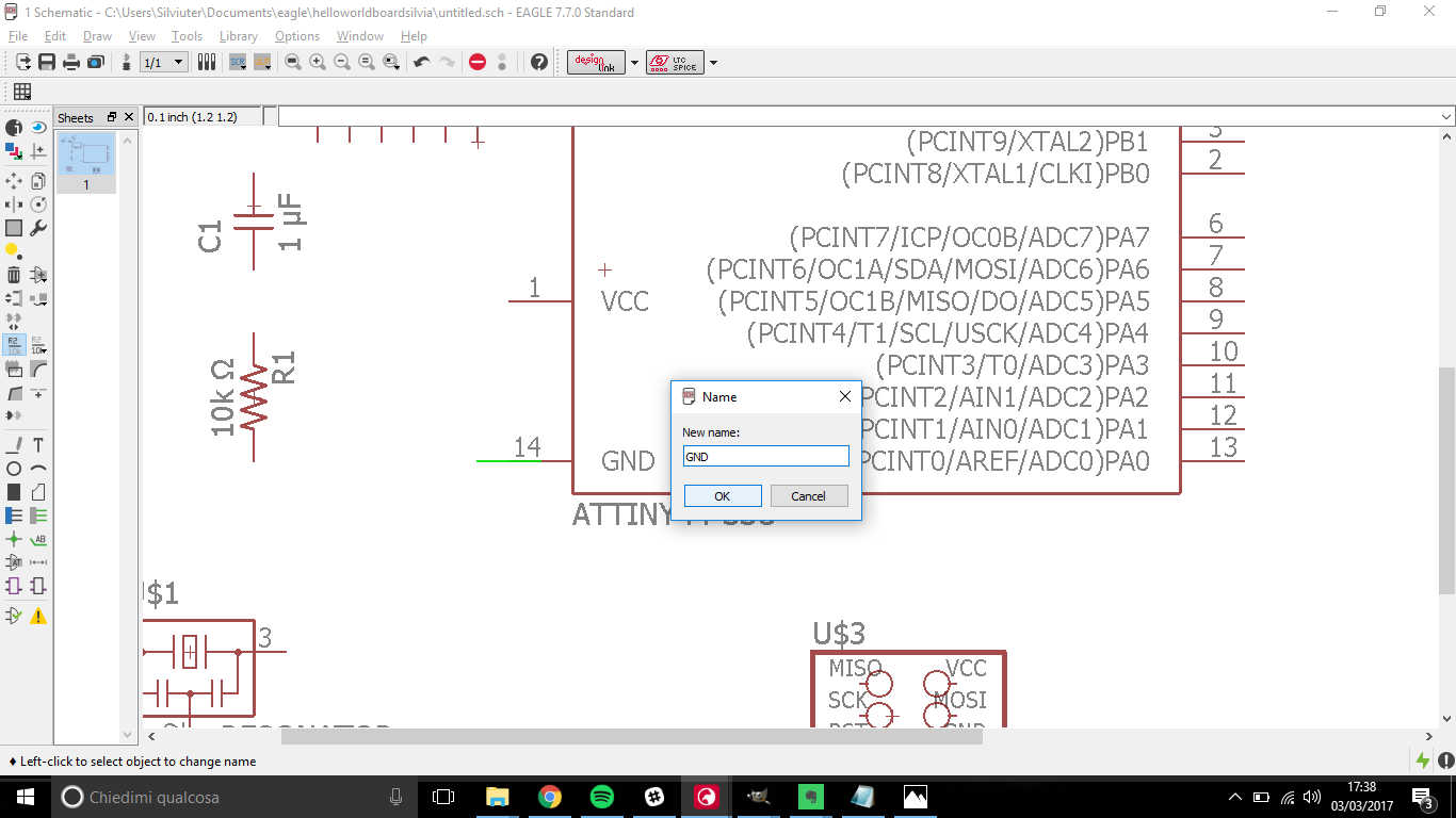
- please note that XMEGA 16e5 has two GND pins, so I gave them two different names "GND@1" and "GND@2", because typing "GND" for both gave an error;
- dimensions and proportions of real components aren't necessary in this step, the symbol can be as big as much you feel comfortable in positioning pins
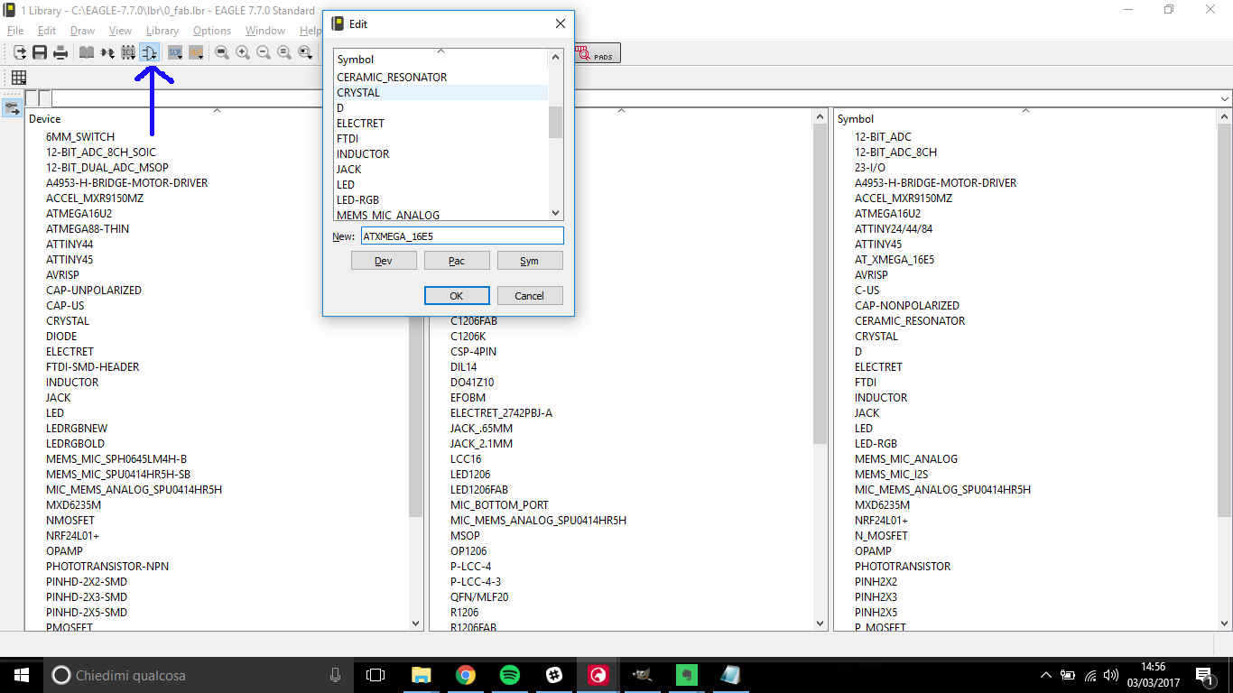
Create a device
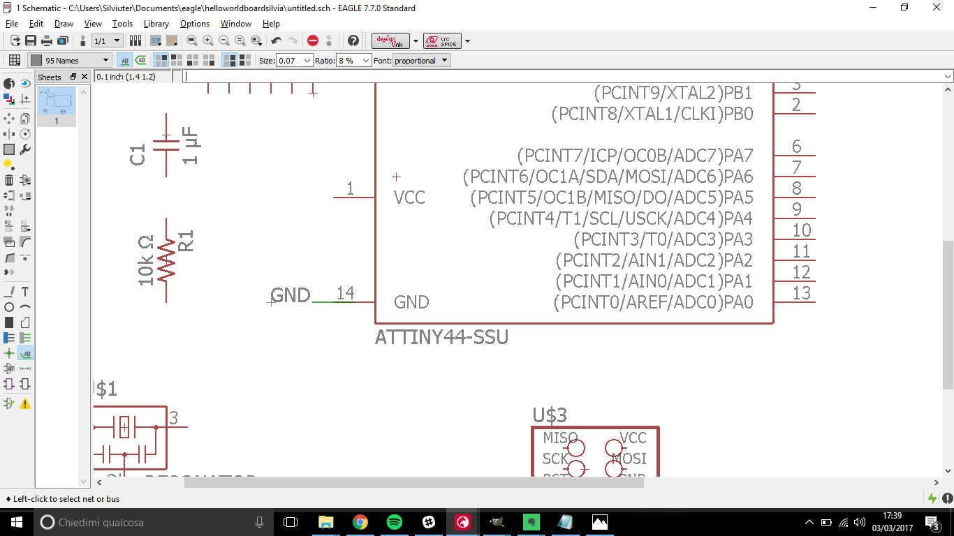
Now that I had both package and symbol, I had to make them communicate somehow.
In fab.lbr I pressed on Device button and added a new one:
 I then added the symbol I designed...
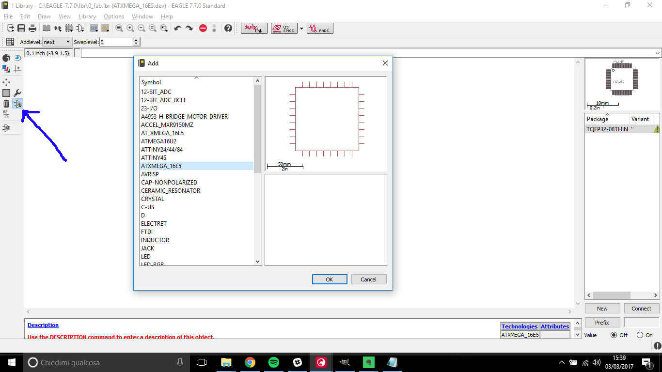 ...and the standard package (by clicking on New in the bottom of the window on the right
 Then, by clicking on Connect -close to New- a new window helps you in associating pin and pads:
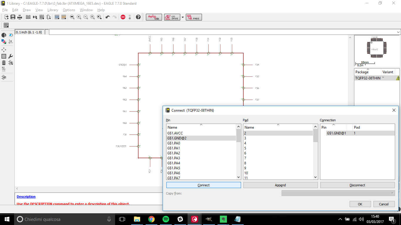 NB: pay attention to this passage, give a look to datasheet
pin number and care not to confuse pin names and numbers!
NB: pay attention to this passage, give a look to datasheet
pin number and care not to confuse pin names and numbers!
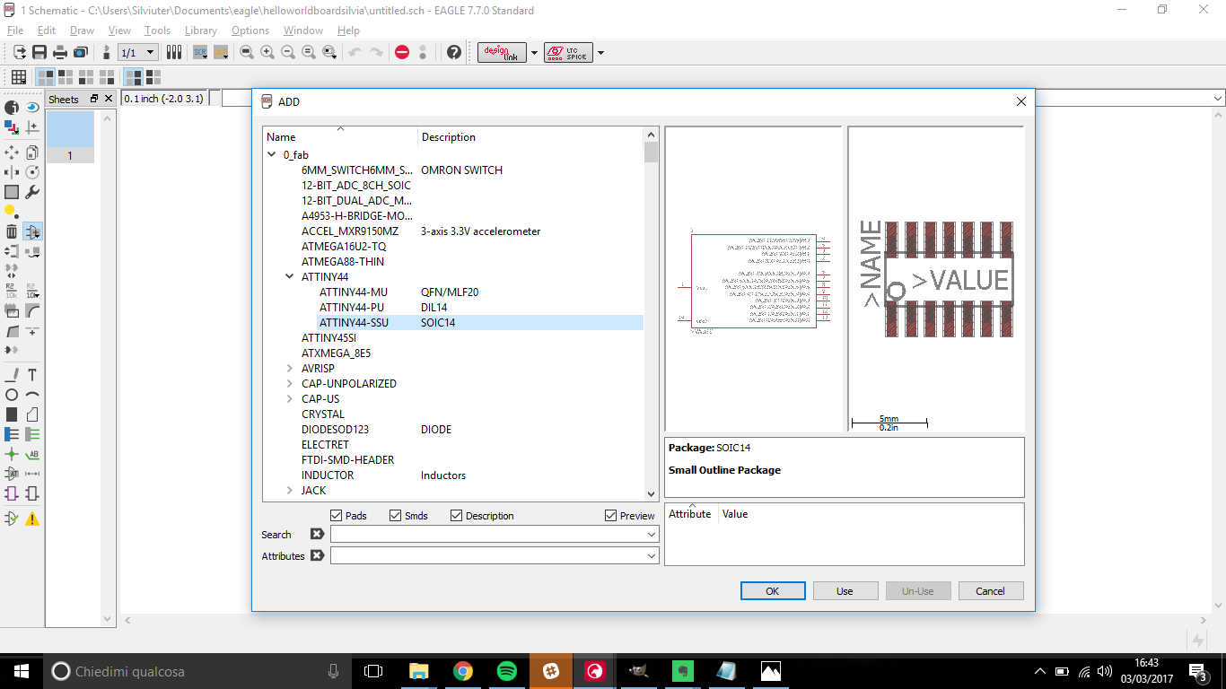
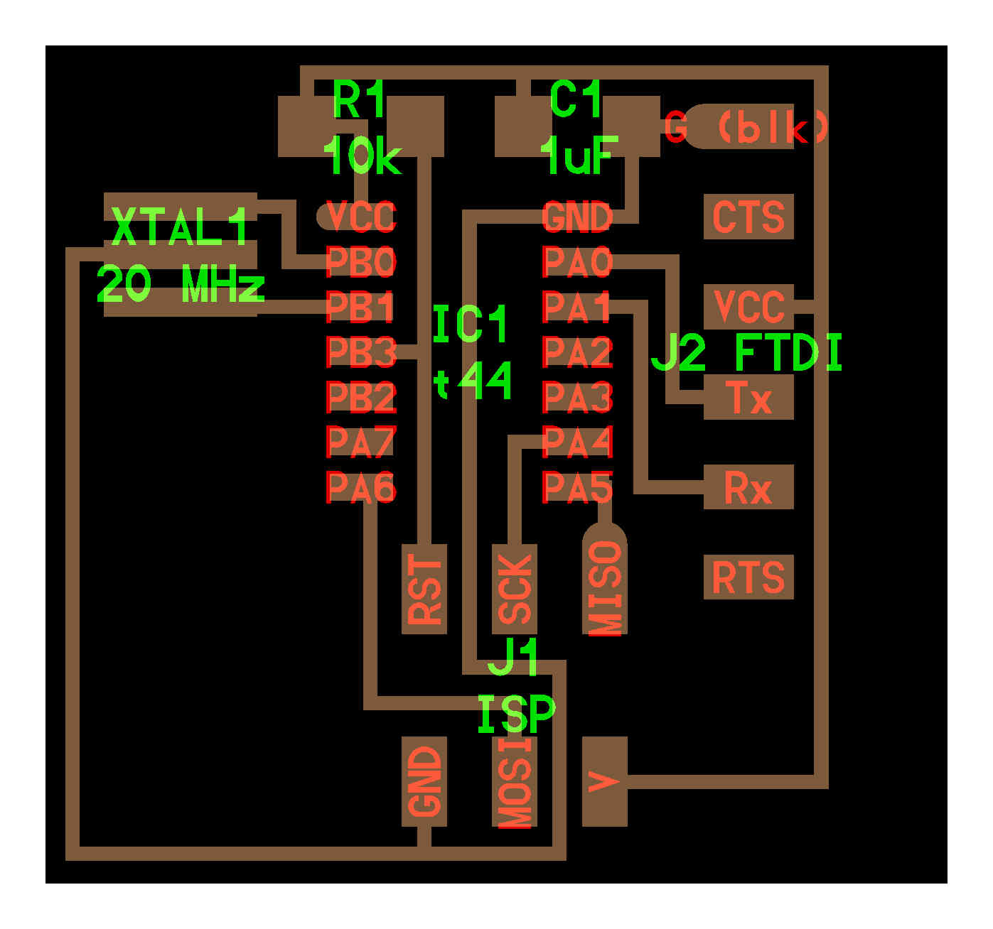
ATtiny44 version
General info
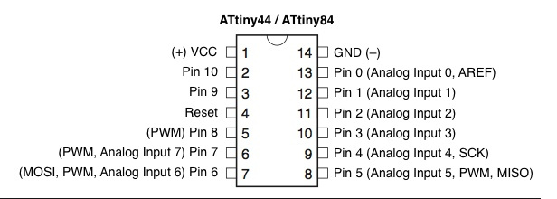
ATtiny44 is quite different from XMEGA 16e5 only just at first glance: 8 vs 32 pins makes a relevant difference in microcontroller potential but little Attiny can go with its head held high. In fact loads of projects have been made with this little 8 bit-microcontroller. I found a detailed description of Attiny features but I still have to study a bit most characteristics meaning still.
Components list
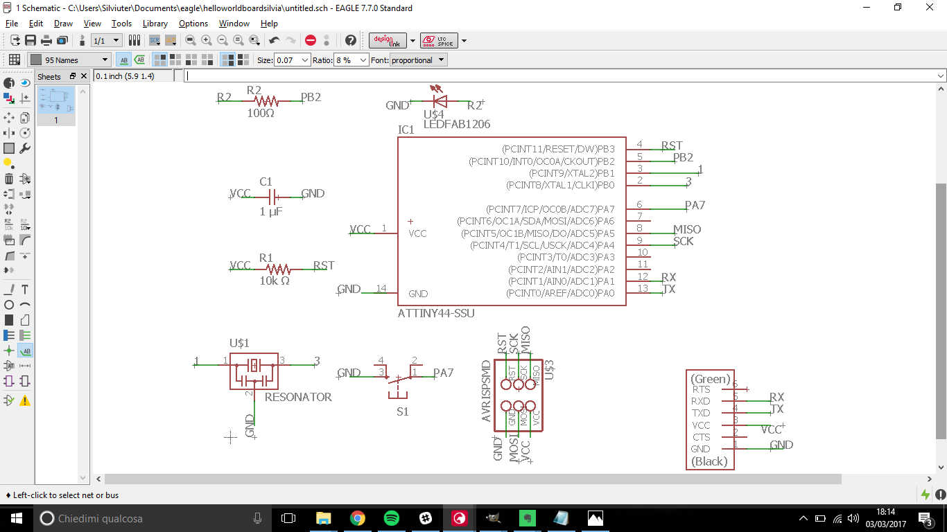
As for XMEGA 16e5 hello board, I wanted to make myself an idea about components and how they were linked:
 I then wrote down my BOM:
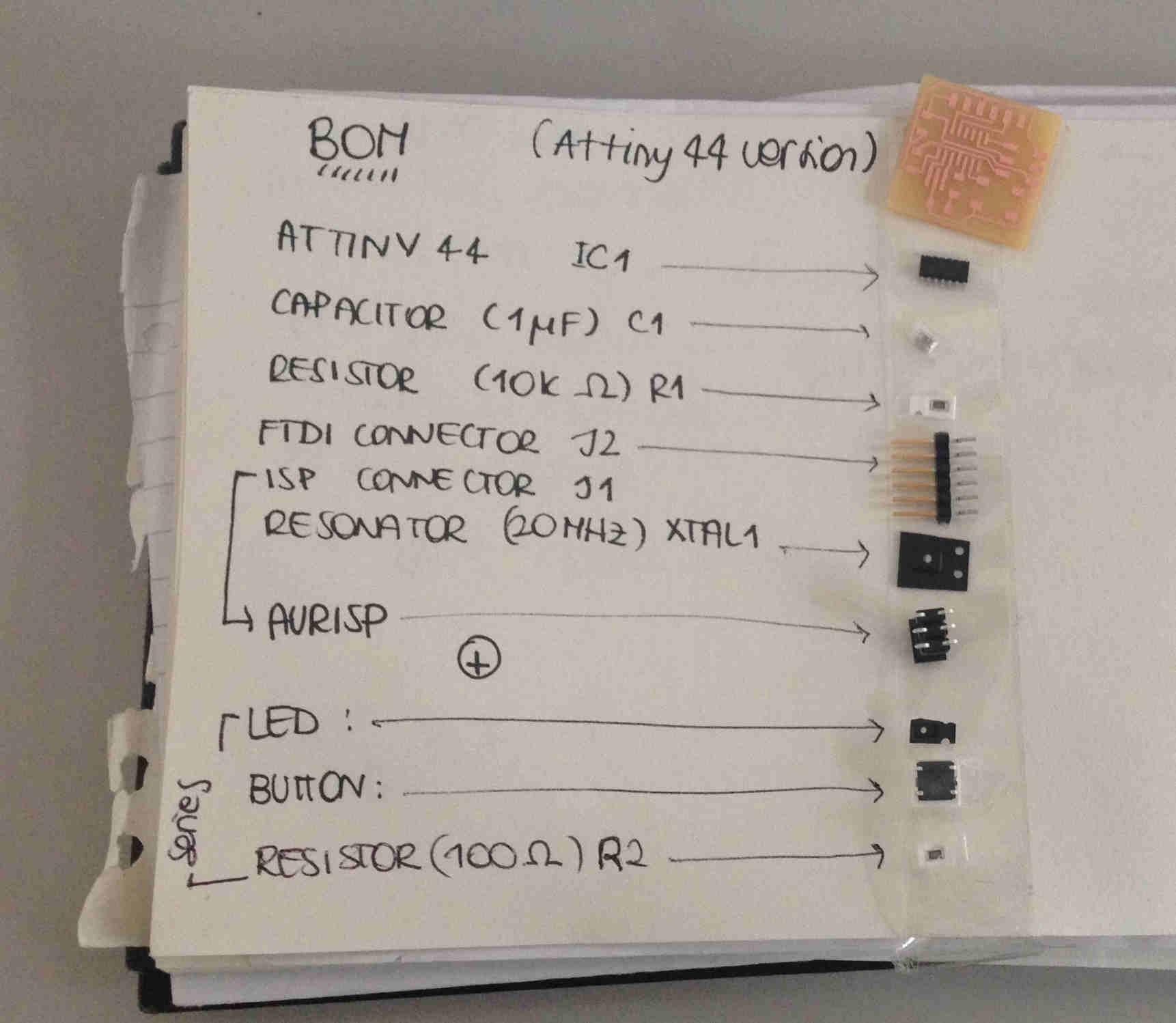 To this list I had to add an LED and a button. As for this last one element, I found great help in reading
Omron's switches datasheet for what regards linking and kind of switch - mine was without grpund terminal-.
To this list I had to add an LED and a button. As for this last one element, I found great help in reading
Omron's switches datasheet for what regards linking and kind of switch - mine was without grpund terminal-.
IMPORTANT: while adding an LED you need to put a resistor in series, otherwise it will get burnt (remember supply voltage is bigger than the one you must provide for LED current need).
To help you calculate which resistor you need, you can simply apply Ohm's law:R=V/I
As for "V" in this case you have to consider the difference between voltage supply and voltage drop along the LED, for "I" you must consider the LED desired one.
So V=(3.3-2)=1.3 V and I=20 mA.
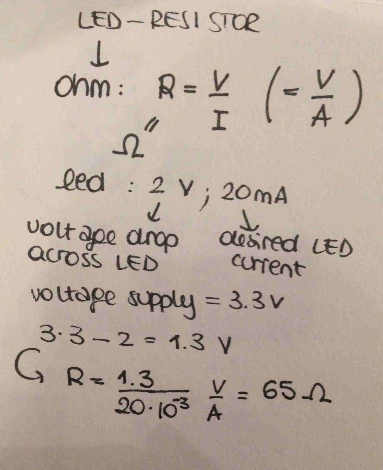 I chose 100Ω resistor cause it was the closest one in value to 65Ω (choosing a lower one would have made my
LED explode, higher resistors compromise only brightness)
TIP Don't feel confident with your calculus? try this website!
I chose 100Ω resistor cause it was the closest one in value to 65Ω (choosing a lower one would have made my
LED explode, higher resistors compromise only brightness)
TIP Don't feel confident with your calculus? try this website!
Schematic design
I was then ready for Eagle, so I opened it and went through File-->New..->Project.
NB:I already had fab.lbr installed (see above "EAGLE 7.7.0: import libraries and
examples" if needed)
My project appeared on the left column of the workspace and I opened a new schematic inside it (left click on
project name then right click and New..->Schematic). Using the ADD symbol you can put components
on the workspace:
 Repeat this for all components:
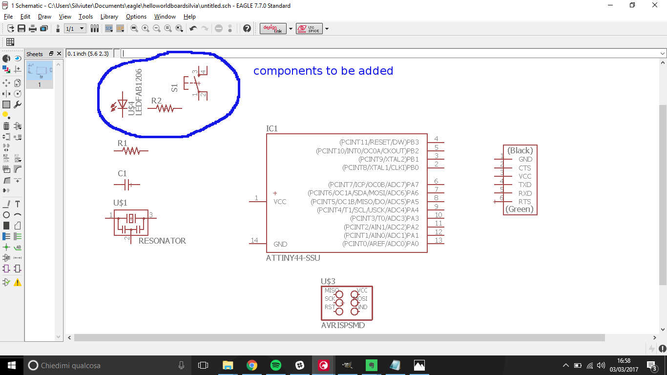 Then you have to link pins of different components; to make it easier, start from hello board .png file:
 Commands to be used are:
- NET: that creates link;
- NAME: that assign a name to the link;
- LABEL: that shows link name in a label;
- VALUES: for optional definition of quantities and units of measurements (see R2 resistor in my case).
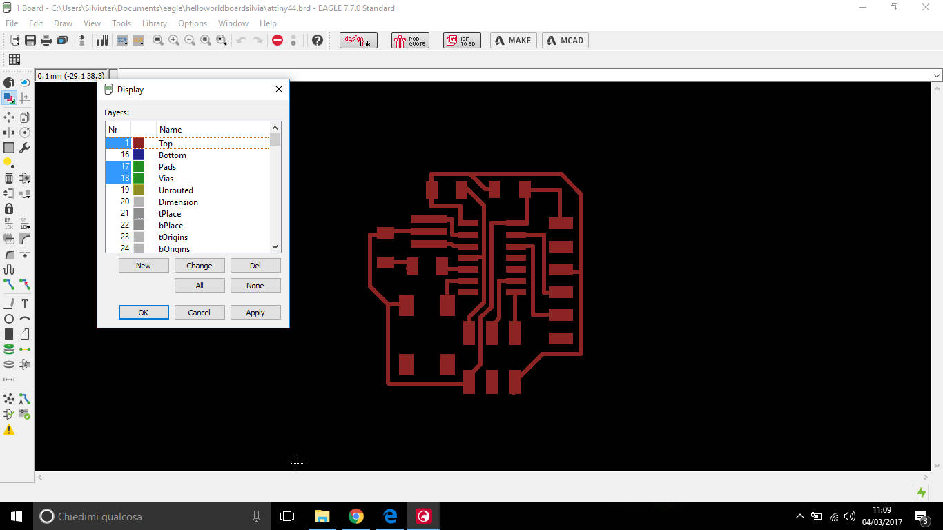
2.3 Board design
Here I found a good tutorial to get started.
I advice you to double-check connection and just after that switch to board visualization
(now connections will be displayed with yellow lines)
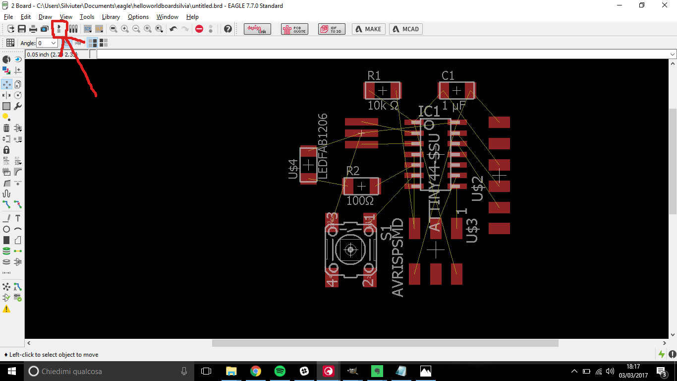 Yellow lines have to be switched to traces that can be drawn with ROUTE command.
 NB: If after routing, you still notice yellow lines, like this...
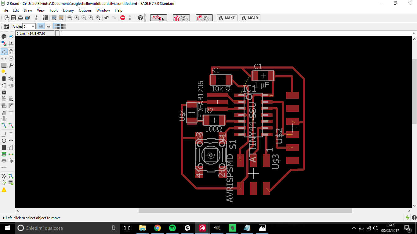 ...check red lines really snapped to pins.
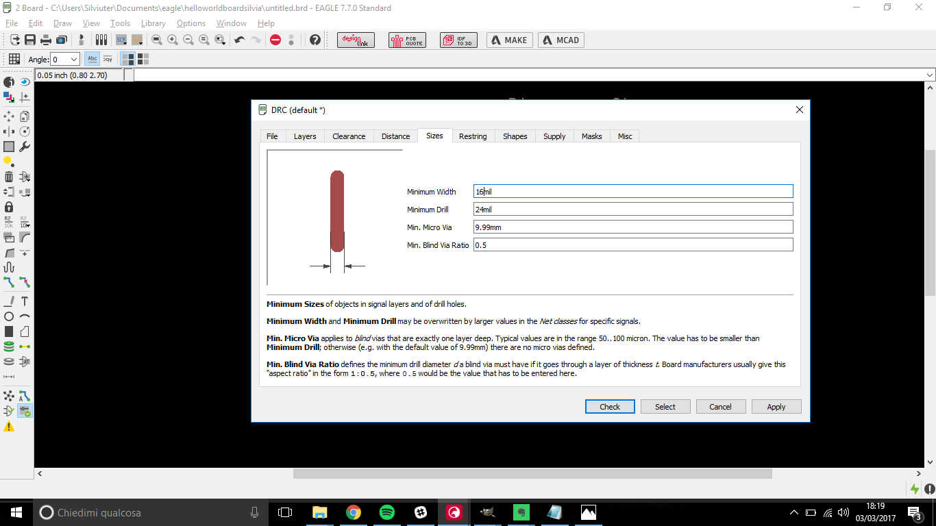
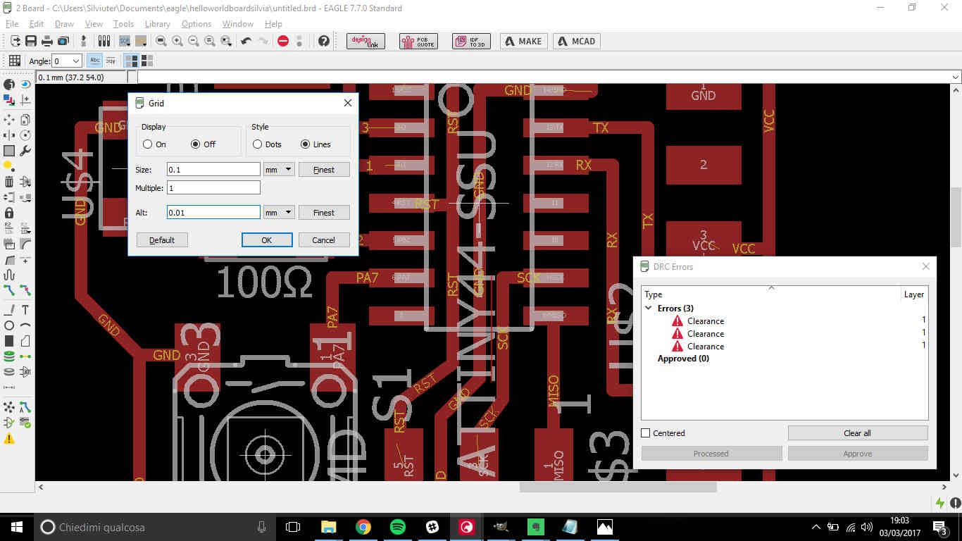
Then it comes to DRC rules: in this part you can set routes characteristics to suit endmill dimensions
(you can set them before or after routing)
 I changed Clearance and Size properties:
![]()
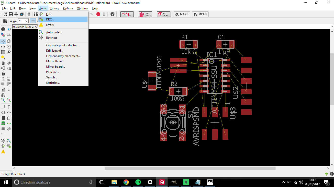
 To check if your routing suits DRC rules go through Tools-->DRC and click Check in new window.
Errors will be displayed with red lines.
To check if your routing suits DRC rules go through Tools-->DRC and click Check in new window.
Errors will be displayed with red lines.
TIP: when you have several lines to pass in a strict path, changing grid
can helps you in tiny movements. Also, press Alt button while moving will gave you a precise drag and drop.
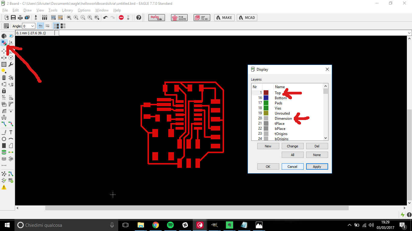
Export a board from EAGLE
You than have to export board design as .png file so as to be send to fabmodules. To do
that, you just need some layers of the design.
Don't follow these steps
I made a mistake the first time I exported layers,
and I gained bad results in milling. In fact, I selected Top and Dimensions
layers:
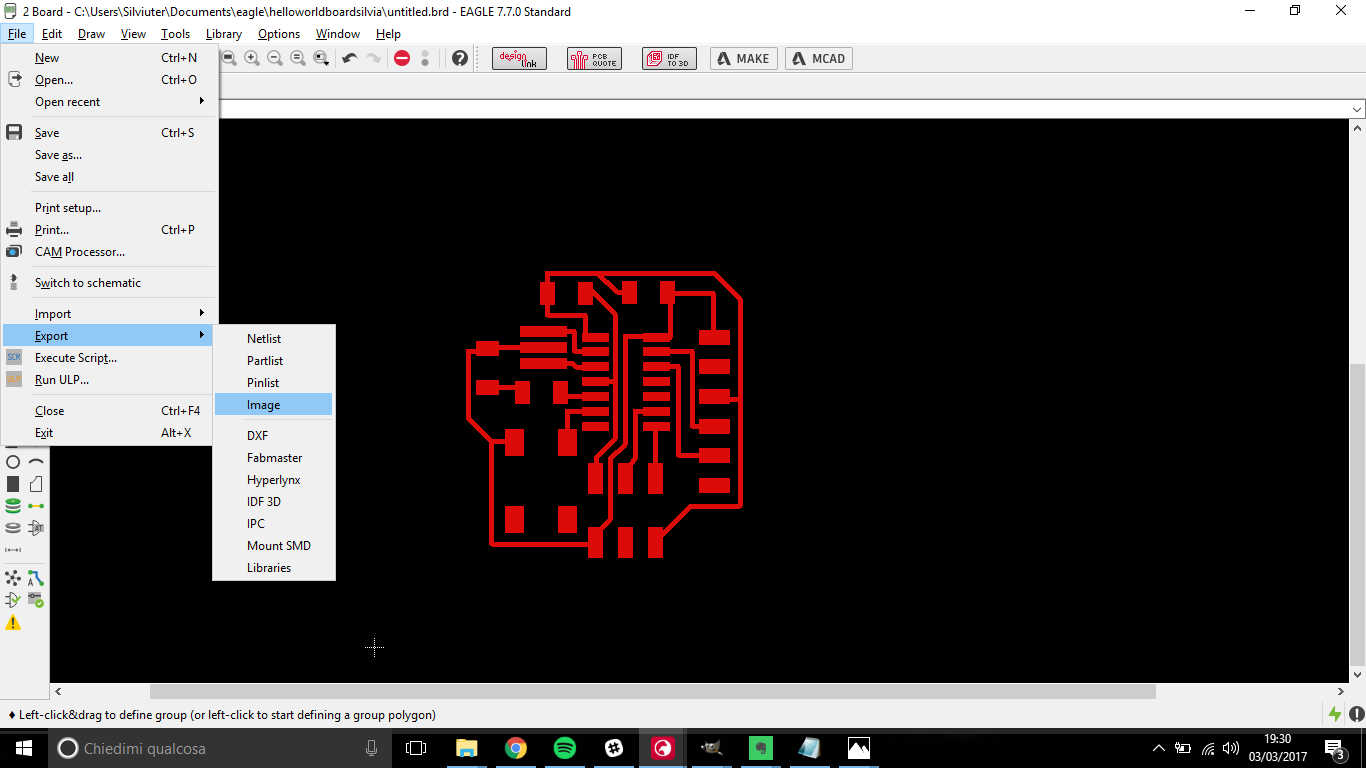
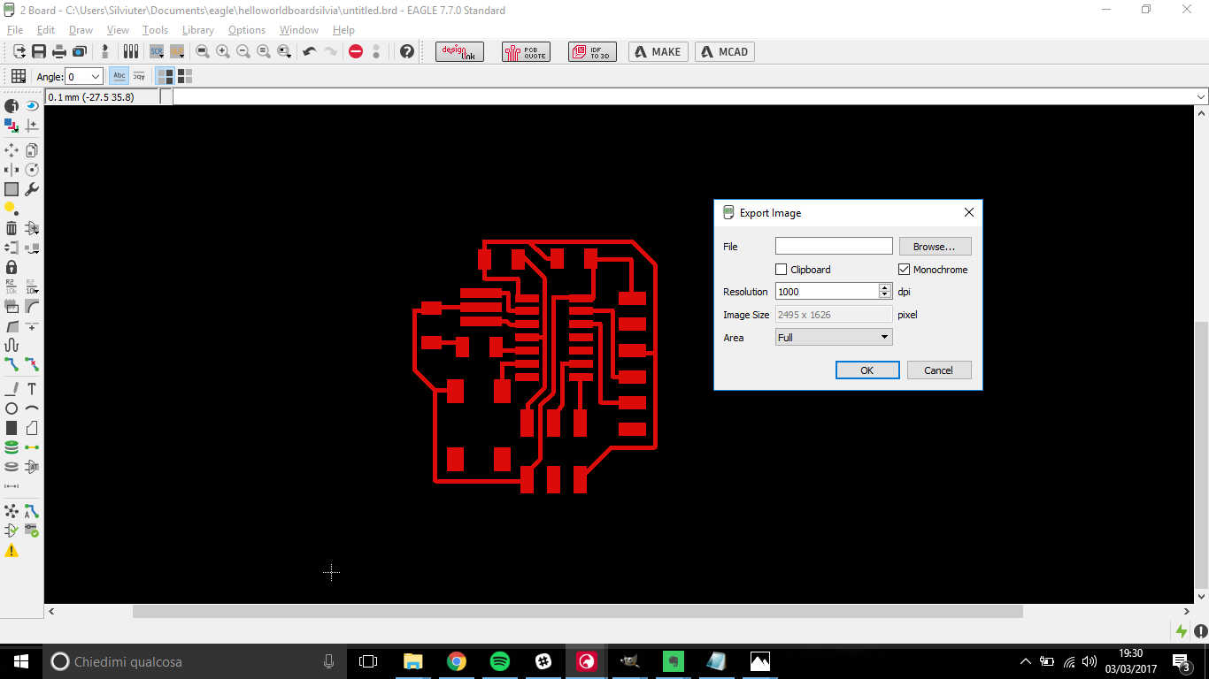
 Then, to export the image I went through File-->Export..->Image and set dpi (1000 or 500 is ok):
 My problem was that I made an error in adjusting outline and traces .png on GIMP (I will explain below)
and in exporting Dimensions layer, therefore feeding fabmodules with those images
gave bad results in milled PCB: I had no padding between traces and edges.
My problem was that I made an error in adjusting outline and traces .png on GIMP (I will explain below)
and in exporting Dimensions layer, therefore feeding fabmodules with those images
gave bad results in milled PCB: I had no padding between traces and edges.
 I then fixed the mistake on GIMP but I still had padding error on a side, so it depended on EAGLE image
exportation:
I then fixed the mistake on GIMP but I still had padding error on a side, so it depended on EAGLE image
exportation:
Follow this procedure
I talked about my problem to my instructor, who supposed the mistake came from wrong layers exportation. To him, the ones I had to consider where Top, Pads and Vias layers, so I repeated the procedure above making this change:
And I gained this result:
NB:if you notice something's missing, you're right. I realised I didn't link an AVR ISP pin on EAGLE, just after twice trying to test the board.
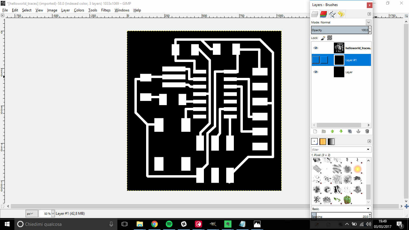
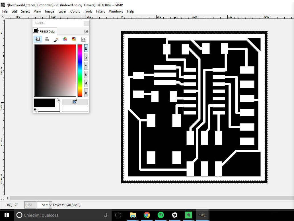
Using GIMP to edit a board .png
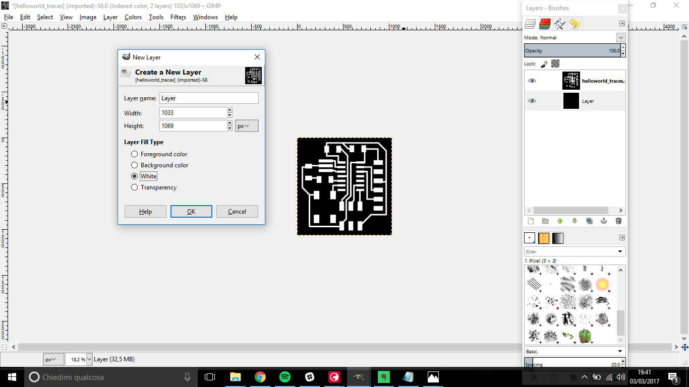
Once I had .png file I had to make them ready for fabmodules. There's simple process to follow on GIMP:
- open image;
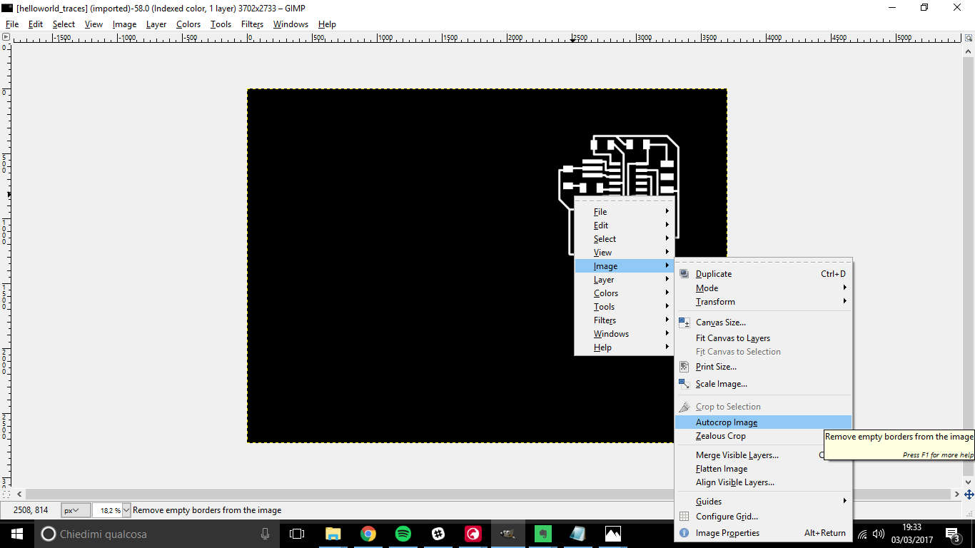
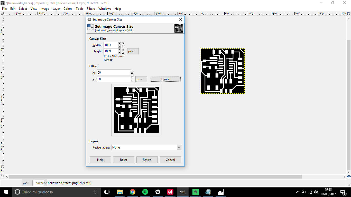
- right click: Image-> Autocrop Image;
- right click: Image-> Canvas Size;
- in window opened, add 100 px per each dimension and click on Center;
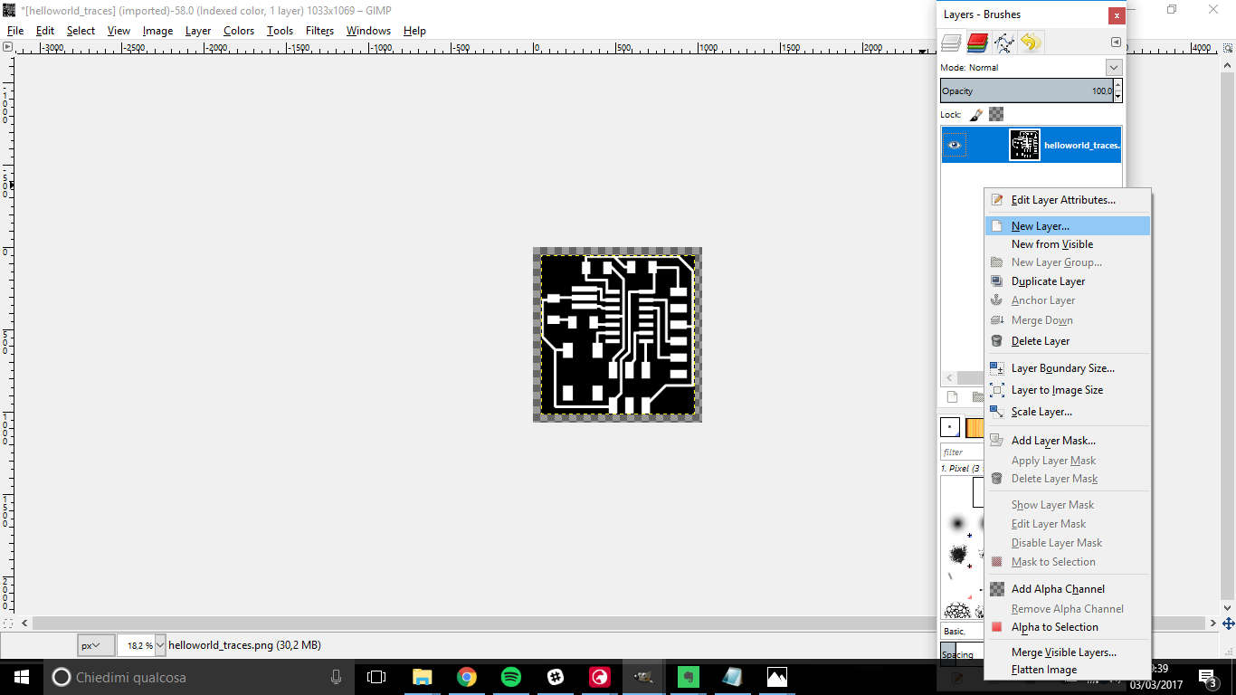
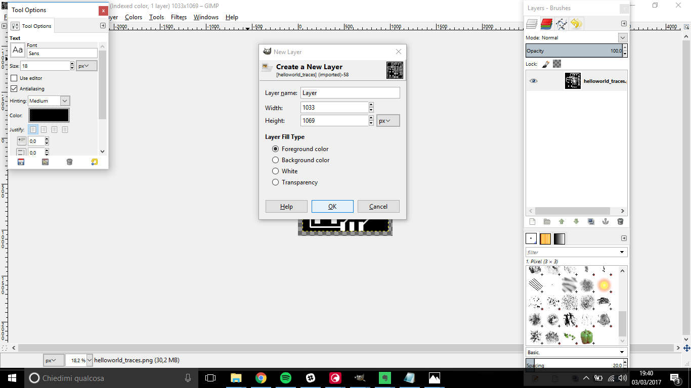
- right click in Layer window on the right: New Layer..-> Foreground color;
- drag and drop new layer under the starting one;
- right click in Layer window on the right: New Layer..-> White;
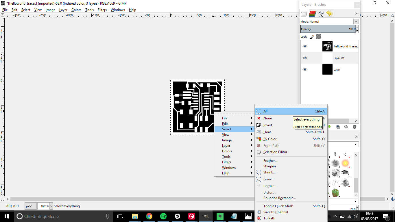
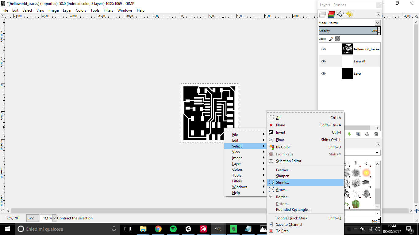
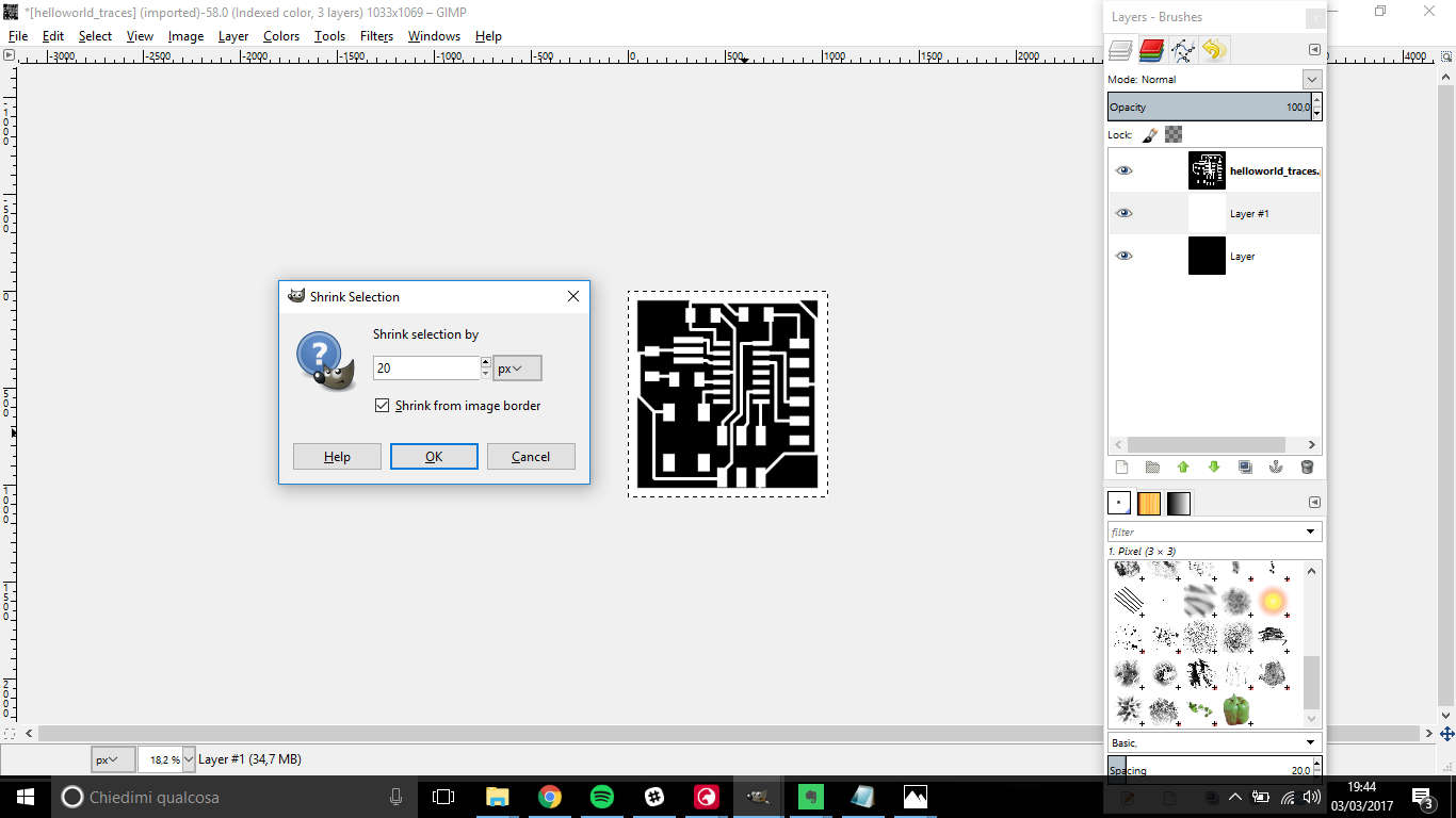
- right click on the image: Select-> All;
- right click on the image: Select-> Shrink and set 20px shrink;
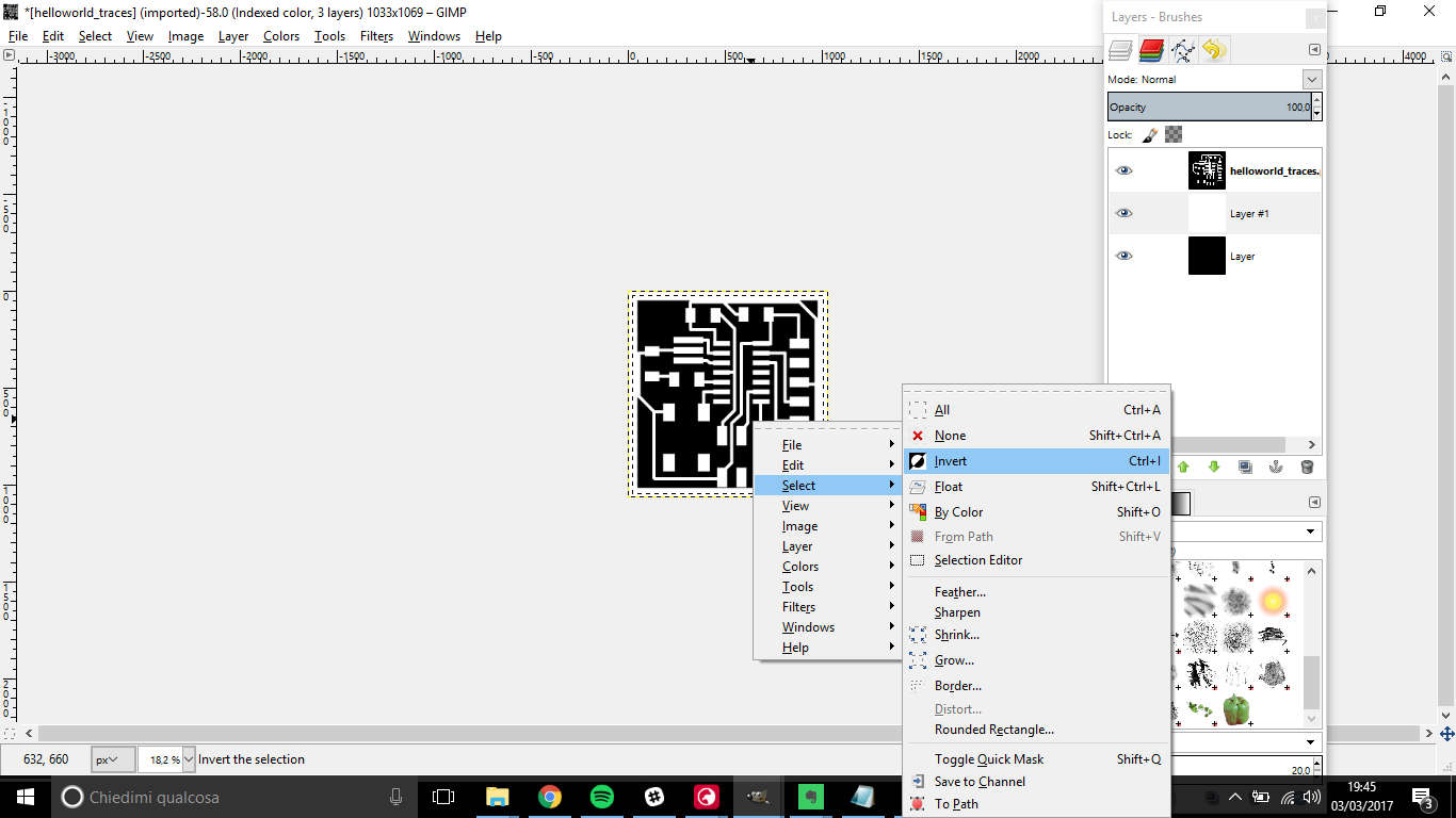
- right click on the image: Select-> Invert - check a border is flashing;
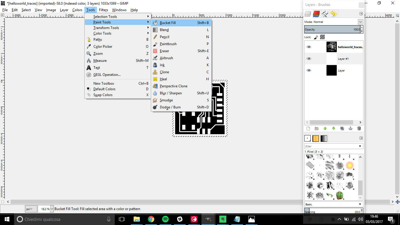
- go through Tools--> Paint tools-> Bucket fill and set black color;
- fill in the flashing border with black;
- export first traces and black layer (hide white layer): this will be traces .png file;
- export white and black layer (hide traces layer): this will be outline .png file;
NB:I still have a doubt about outline .png file: should it be white bordered with black inside or the other way up? Until now, I have proofs to say outline milling works in both ways ( because in week4 I used black filling while I had the best result of hello board using white infill). Theoretically, Roland SRM-20 mills what in black and leaves what in white but I will try to make more experiments to discover best case to use. In any case for black and white drawing it doesn't matter a lot since on fabmodules there's an option to invert colors.
Below, screenshots of GIMP procedure:
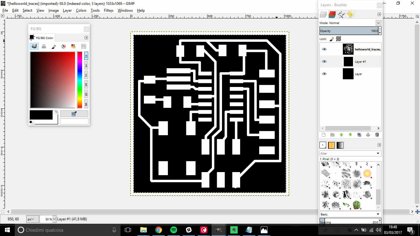
White border and black infill:
Black border and white infill:
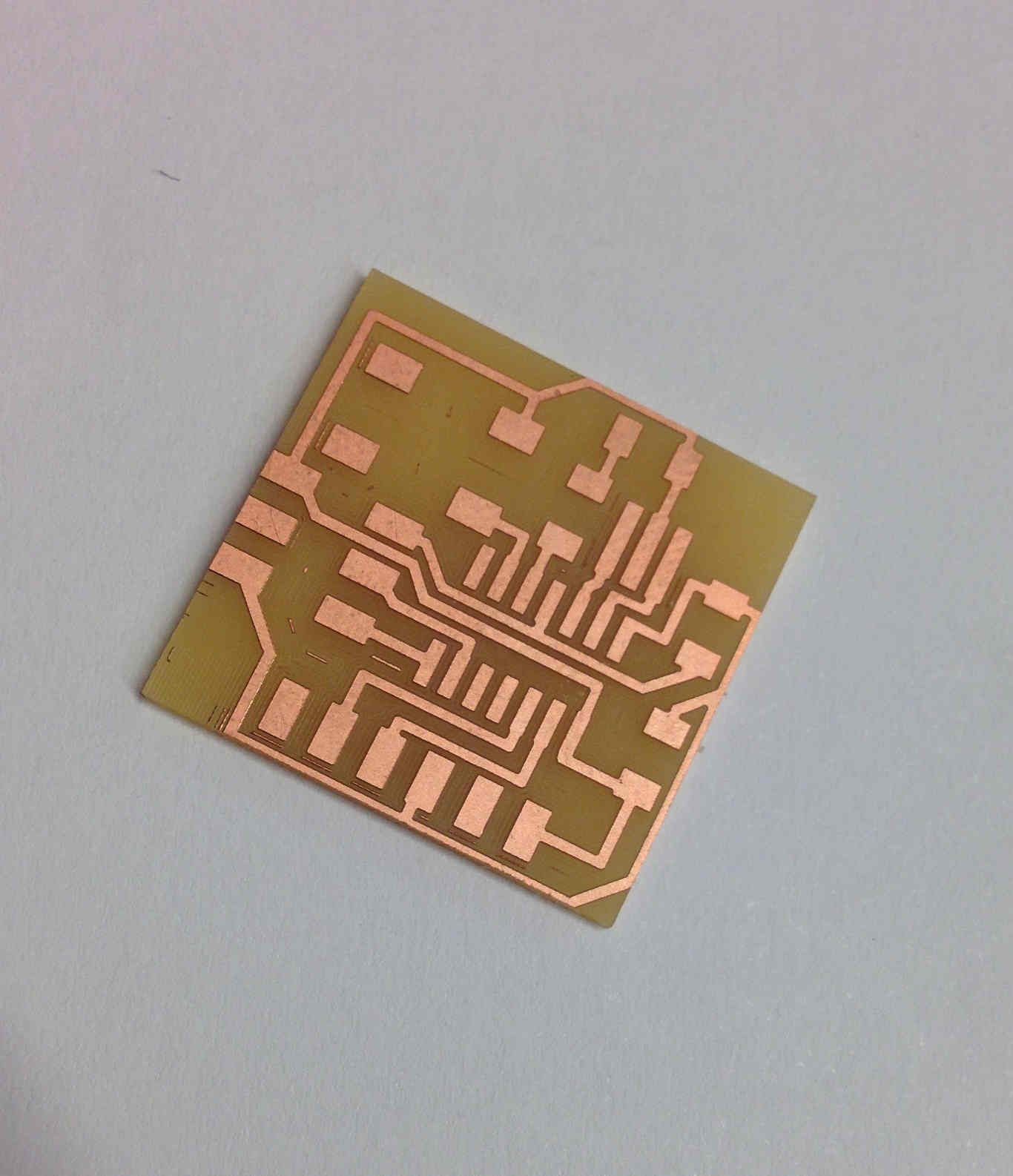
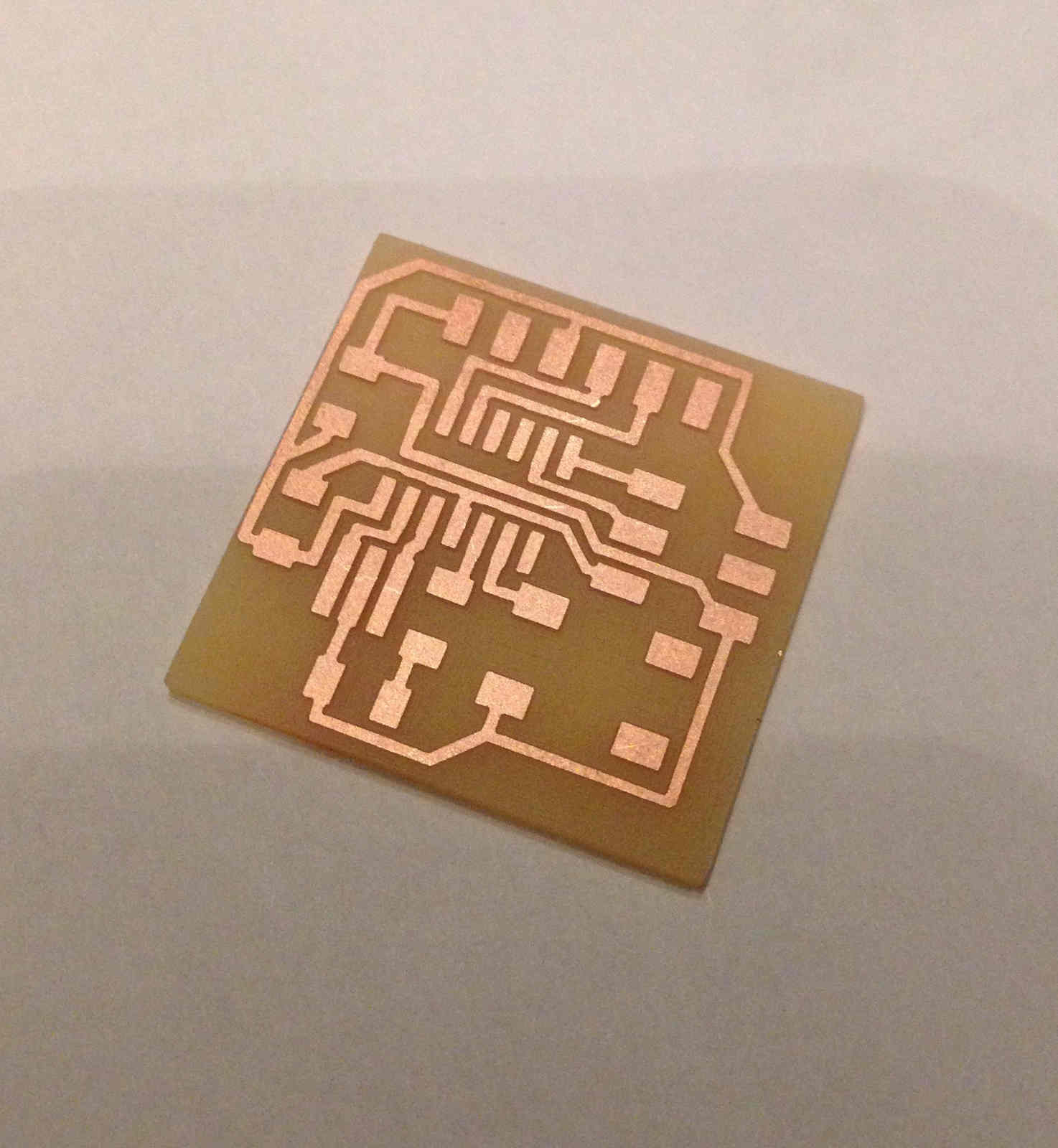
PCB milling
For milling procedure see week 4.
Soldering
live soldering
To see soldering procedure have a look at week 4.
- heat up traces for a while (I usually count up to 6 sec) before putting solder;
- before placing a component, cover the pad with solder;
- after melting solder, wait 3 or 4 second before removing soldering iron from the pad;
- fix components' opposite pins first, then block the others;
NB: in soldering the LED, check that the green line ehich indicates the cathode
is linked to ground (GND).
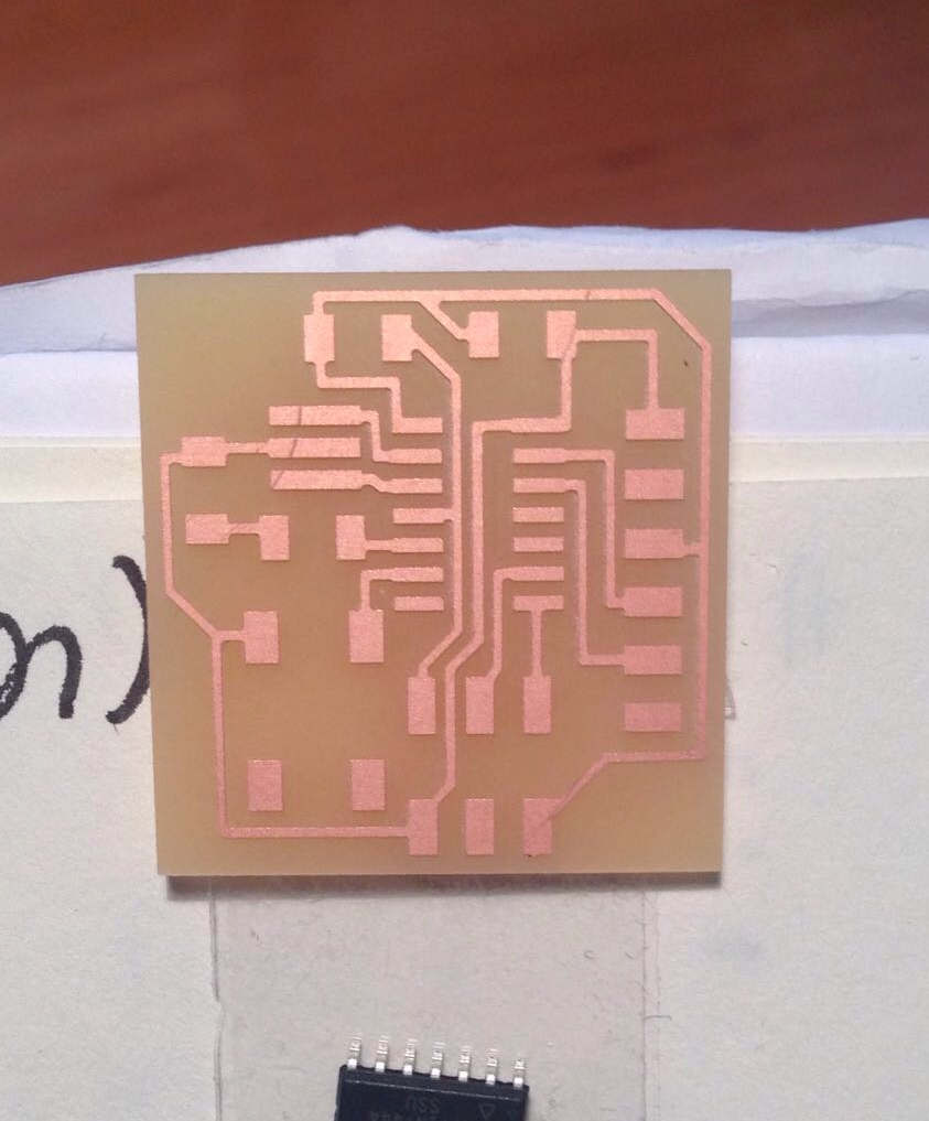
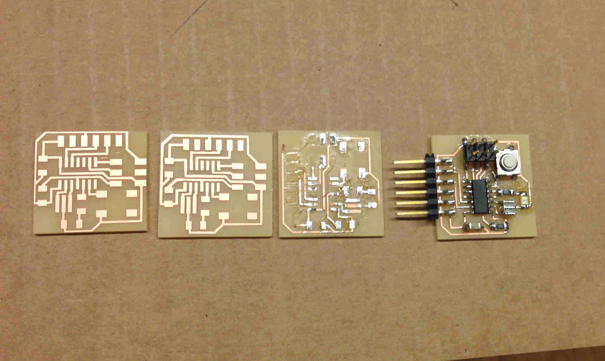
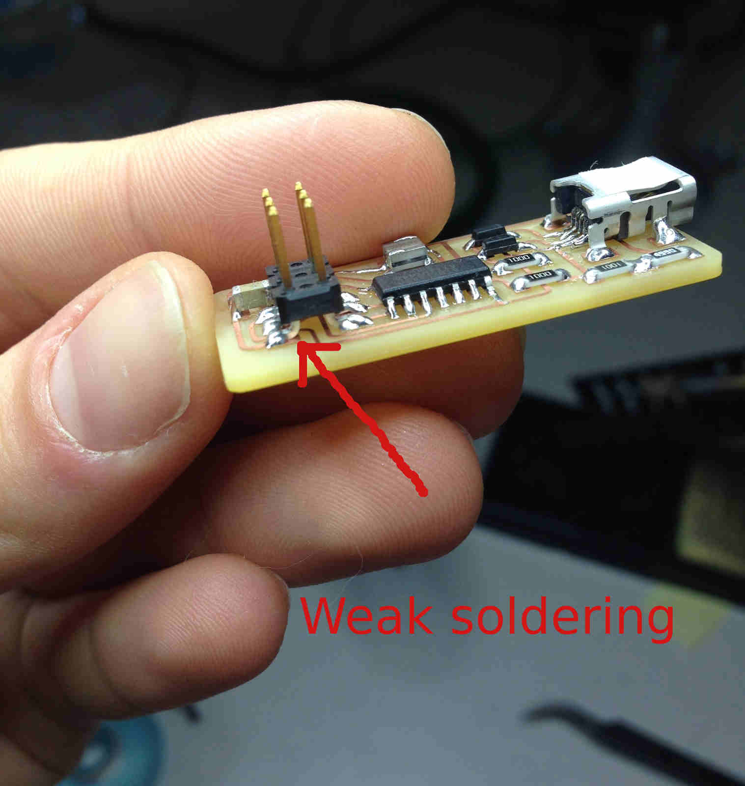
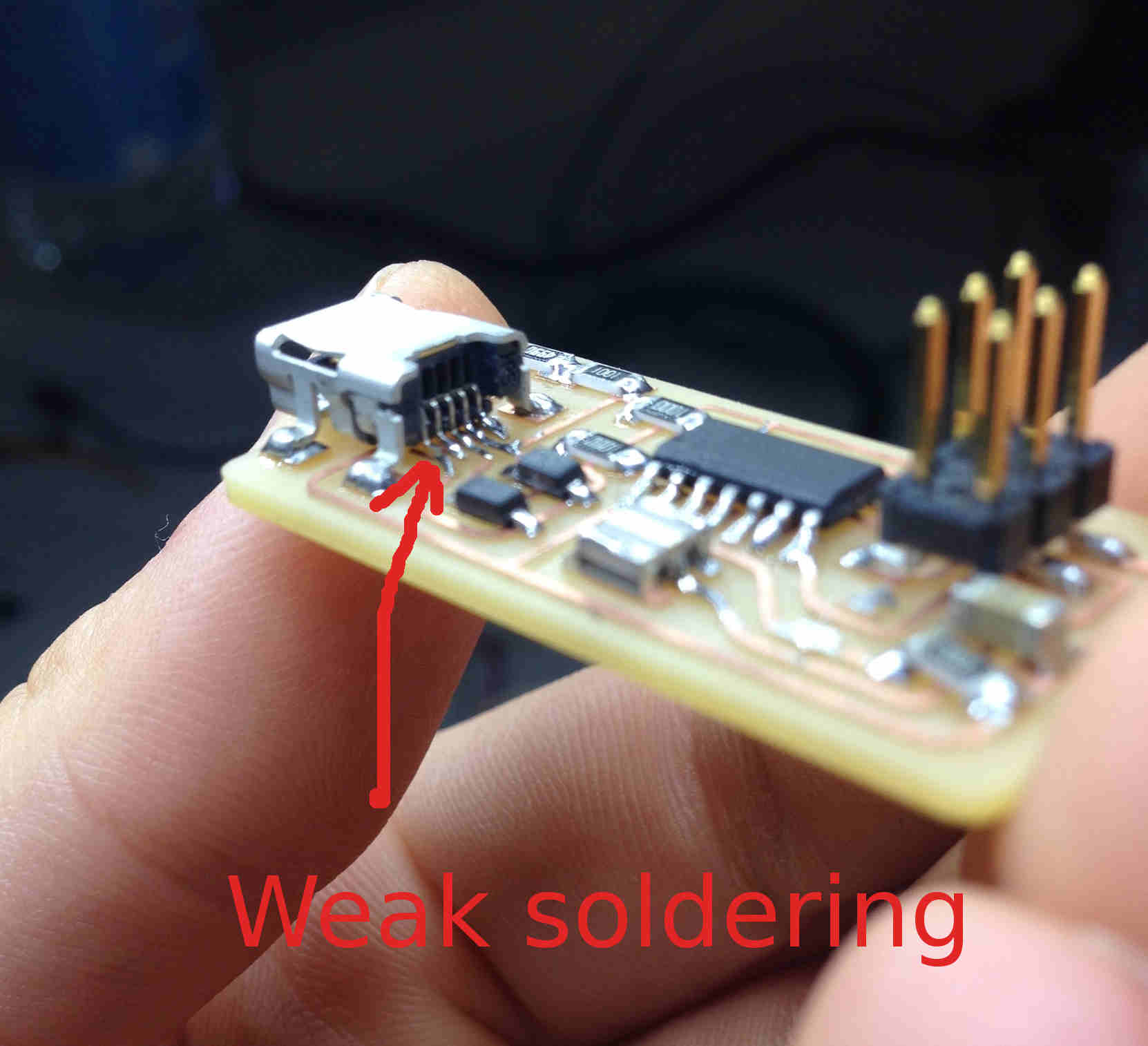
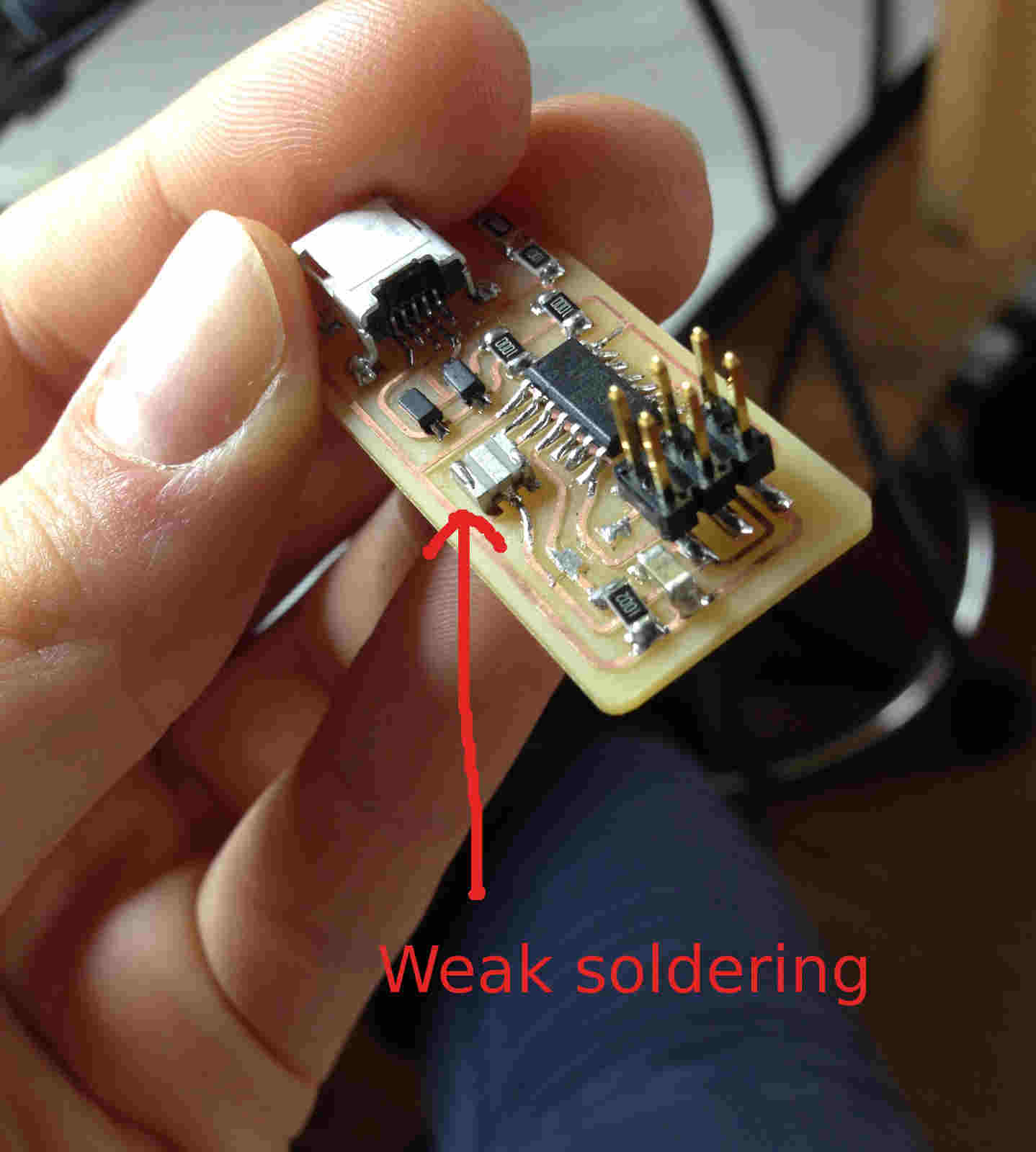
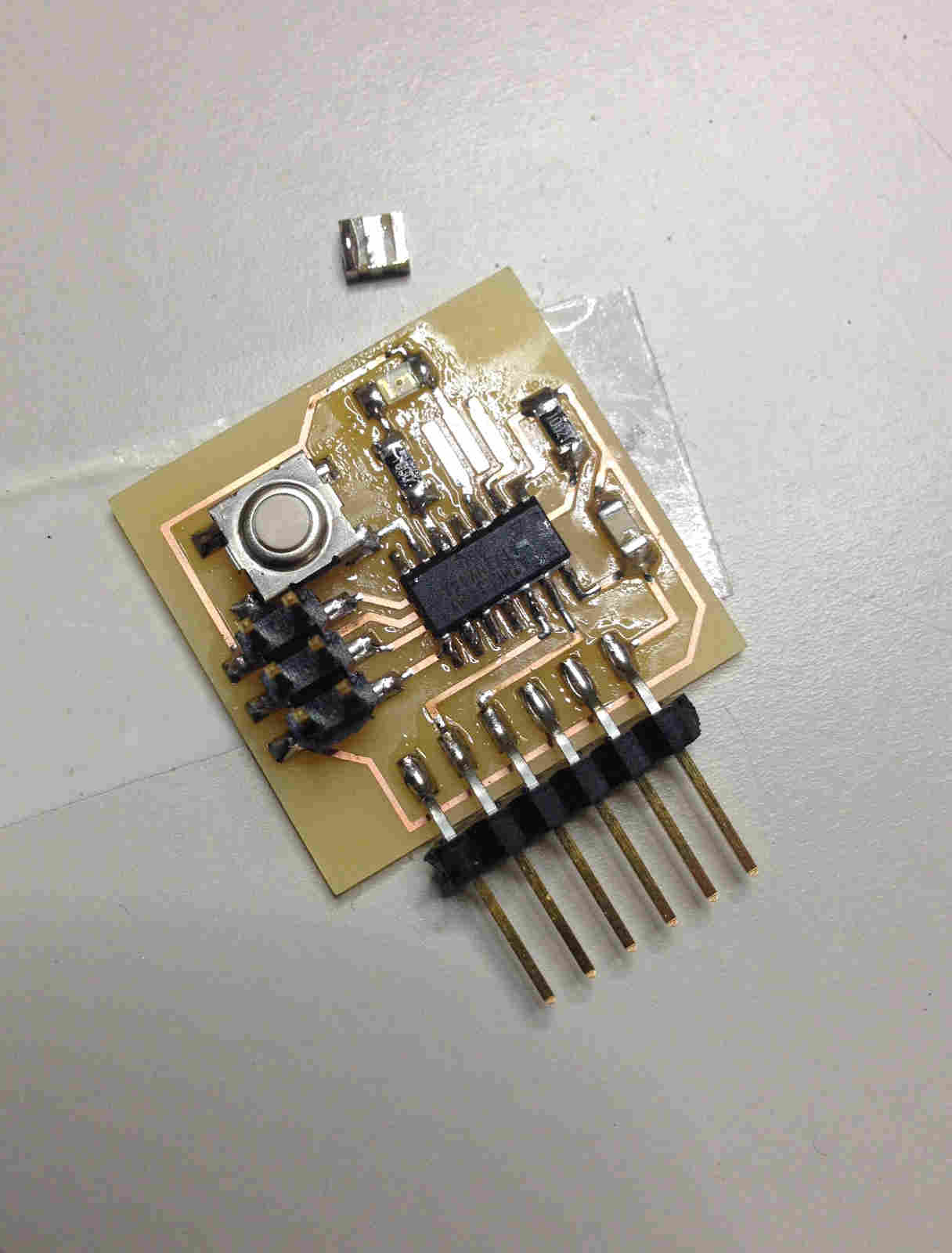
I soldered my board once but in the end, I wasn't satisfied that much of some opaque solderings and I also
realized that Reset pin of Attiny44 lacked of solder:
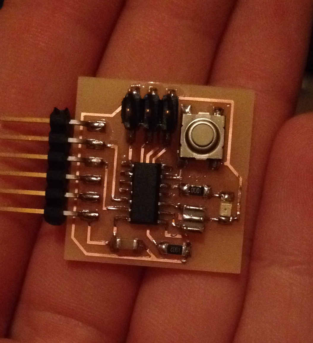
The problem was that the pad I had to fix was just under
microcontroller body.
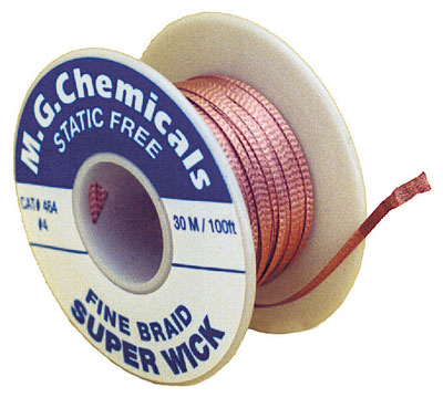
The only chance I saw was to desolder that component,
so I used desoldering wick to do that.
Unfortunately, some of the pads sticked to Attiny44 and many traces split off. I didn't think about
finding a way to fix them (also because the board was really tiny) so I decided to mill a new board and
resolder it.
This time, instead of starting from the Attiny's uppest o lowest pins, I soldered first Reset pin so as not to fall
in previous mistake.
Below I show you my fails:
Hello board programming...Alias what my intention was
I would have liked to program, as extra credit, my hello board.
Make your own connector
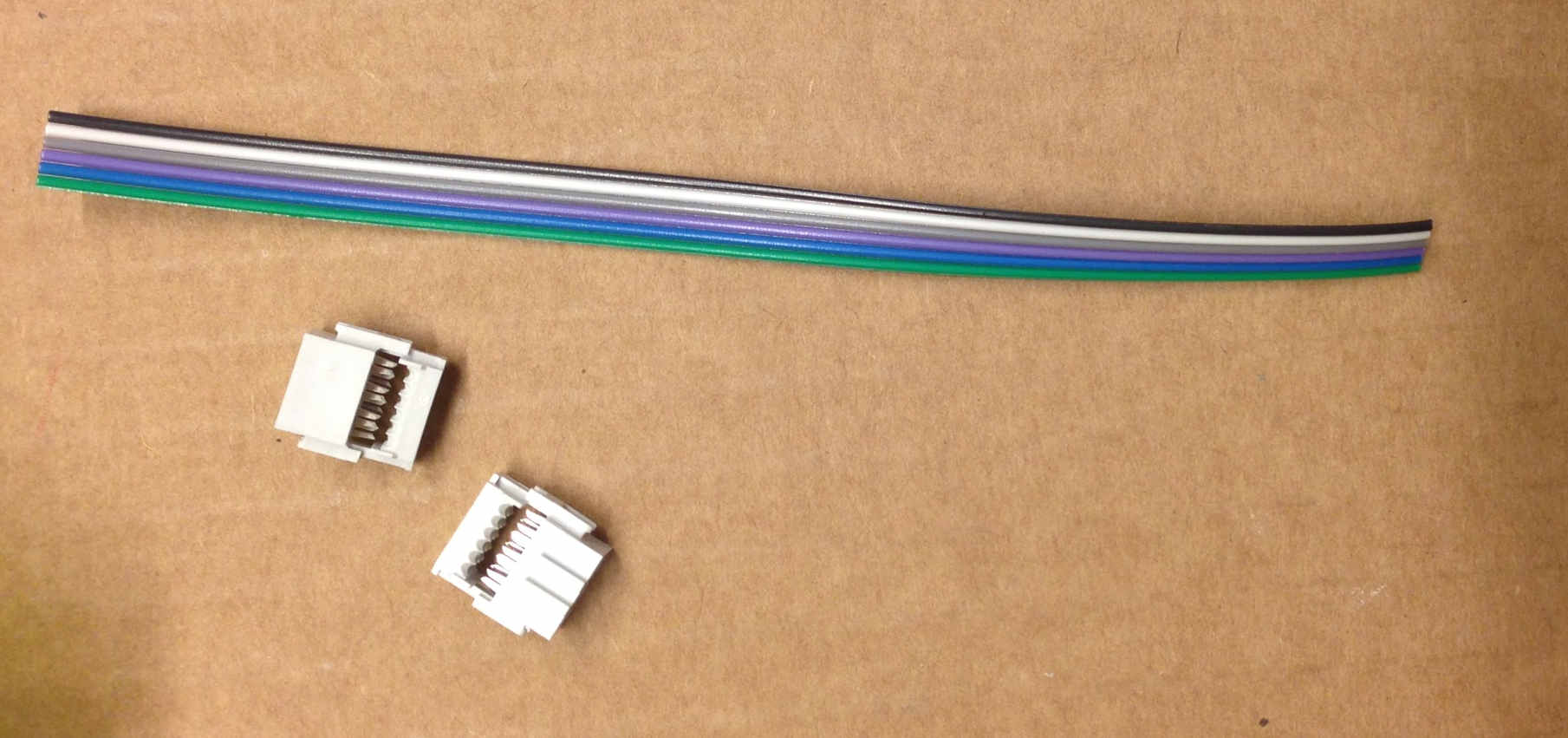
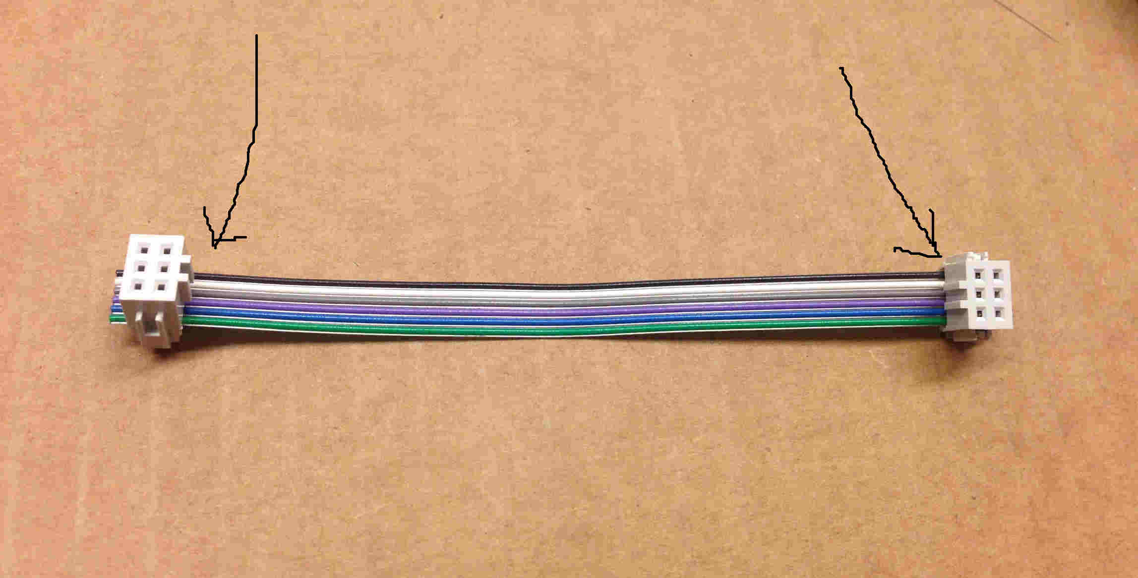
To link hello board and FabISP, I needed to make a wire to connect them.
I used six wires flat ribbon cable and two six wire connectors:
 Savvies:
- check connectors are oriented the right way;
- leave some more wire extra lenght out of the connector so as to test it better with multimeter;
- put multimeter heads in adjacent wires ends (touch inner conductive wires) to check they aren't connected;
- put multimeter heads in wire ends to check it isn't interrupted;
- before closing connectors caps, check each wire enters perfectly metallic choppers;
- press heavily to close caps paying attention not to move ribbon wire
Connector:
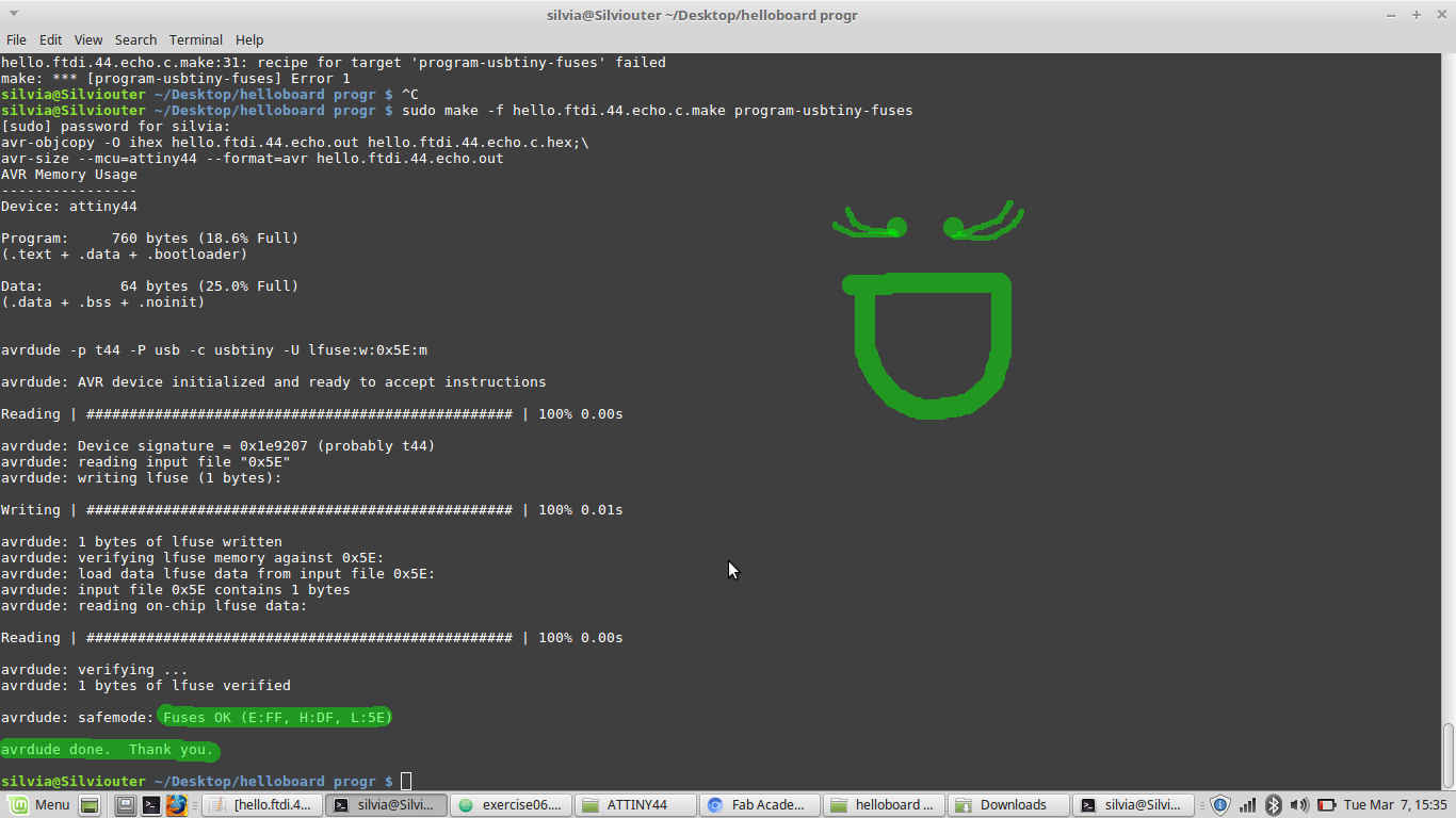
Program the hello board: my being a bumbler results
Referring to ISP programmer process, I created a directory on desktop and put inside it
.make
and .c file.
Then I linked ISP and hello board
From shell, I opened that directory and I ran
make -f hello.ftdi.44.echo.c.make
To understand this command it's better to have a look at .make file:
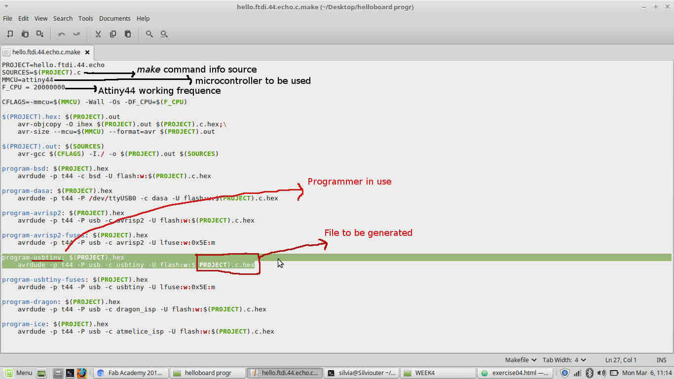 So if you then open main directory, you'll see there are more than the two files imported.
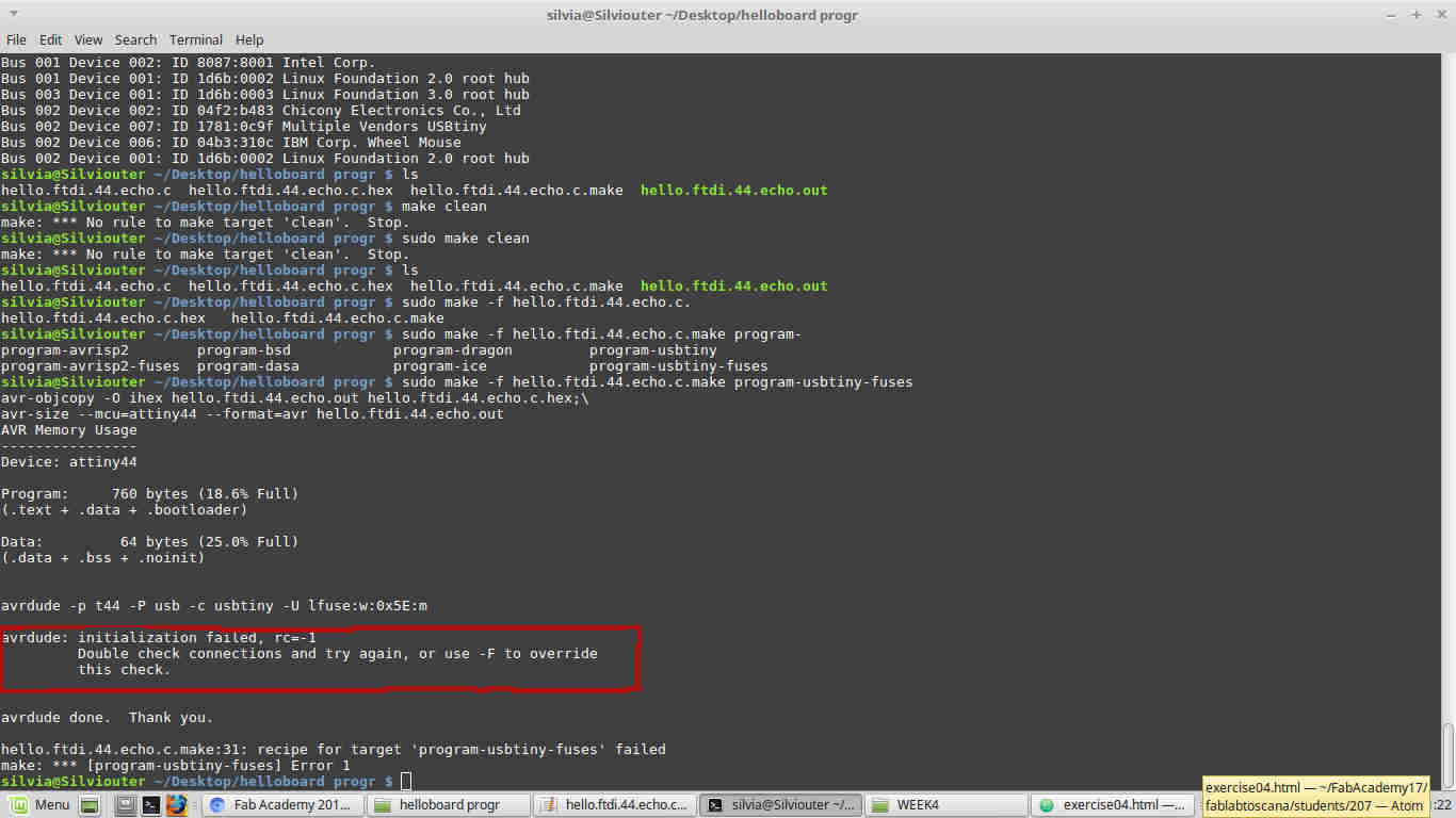
I then ran
make -f hello.ftdi.44.echo.c.make program-usbtiny-fuses
But I got this error:
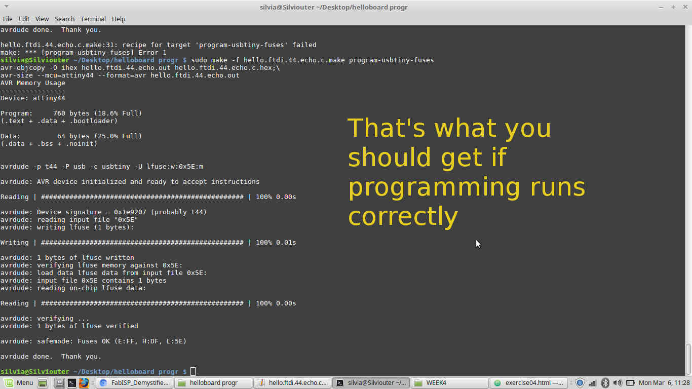
 I then started making test with other boards (which surely worked) to see where my error could come from:
- SILVIA (ISP) + SILVIA (HELLO BOARD) = FAIL;
- SILVIA (ISP) + WORKING HELLO BOARD = FAIL -->Doubt: may my ISP have soldering problems?
- WORKING ISP + WORKING HELLO BOARD = SUCCESS -->Certainty: my ISP has soldering problems;
- WORKING ISP + SILVIA (HELLO BOARD) = FAIL --> Also my HELLO BOARD has soldering problems -.-
Beaten down (but not enough to throw hello board in the air), I started my soldering-fixing plan.
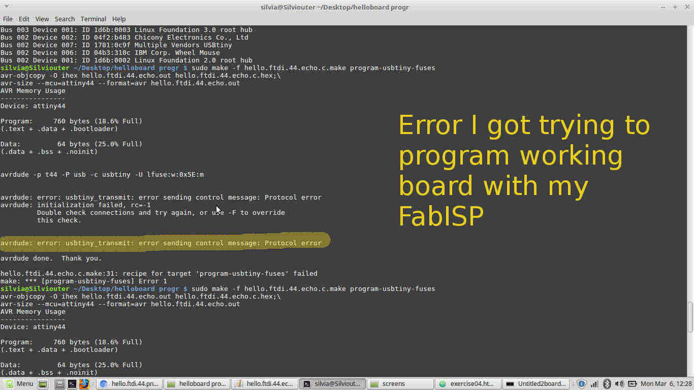
My long debugging journey
Having a look at my ISP and hello board solderings, I started accusing resonators (in both boards) and Fab Optimus's AVR ISP
and mini USB connectors to be programming error's causes (even if not clearly visible,
some pads were not well covered with solder)
 NB: all components are made to resist quite a lot to heat but resonators are maybe among the most sensitive ones to damage,
so I feared I burnt them.
NB: all components are made to resist quite a lot to heat but resonators are maybe among the most sensitive ones to damage,
so I feared I burnt them.

After solderings were fixed (or at least I hoped they were), I re-tested programming procedures and.......(drum rolling)
I successfully sent program with my ISP to working hello board!!!!!
(thriumphant melody and proud clapping)
....but my hello board still had problems :(
DREADFUL EPIPHANY: I didn't net one of AVR ISP pins on EAGLE
(you can seriously start to believe me when I say I'm dumb)
I so followed a shortcut to see if this new problem was the one that endangered my programming process.
I know you want to see the shortcut ;) here you are:
 I then run back to my notebook to try sending data to it and.....
 I feel so cool I wanted to load blinking LED program on it. I'm still working on that
NOTES
- 1-schematic: brief description would say that schematic is a drawing that represents circuits, where wires are conductors and components are shown with their symbols...anyway best to have a look to chapter 6 of Electronics for Dummies by Gordon Mc Comb and Earl Boysen;
- 2-current regulator
- 3-