WEEK 6 - ELECTRONICS DESIGN
Introduction
The assignments of this week were:- Redraw the echo hello-world board, add (at least) a button and LED (with current-limiting resistor), check the design rules, make it (if you have time this week, test it).
- Select and use software for circuit board design.
PCB DESIGN
This week I had to redraw the Echo hello-world board
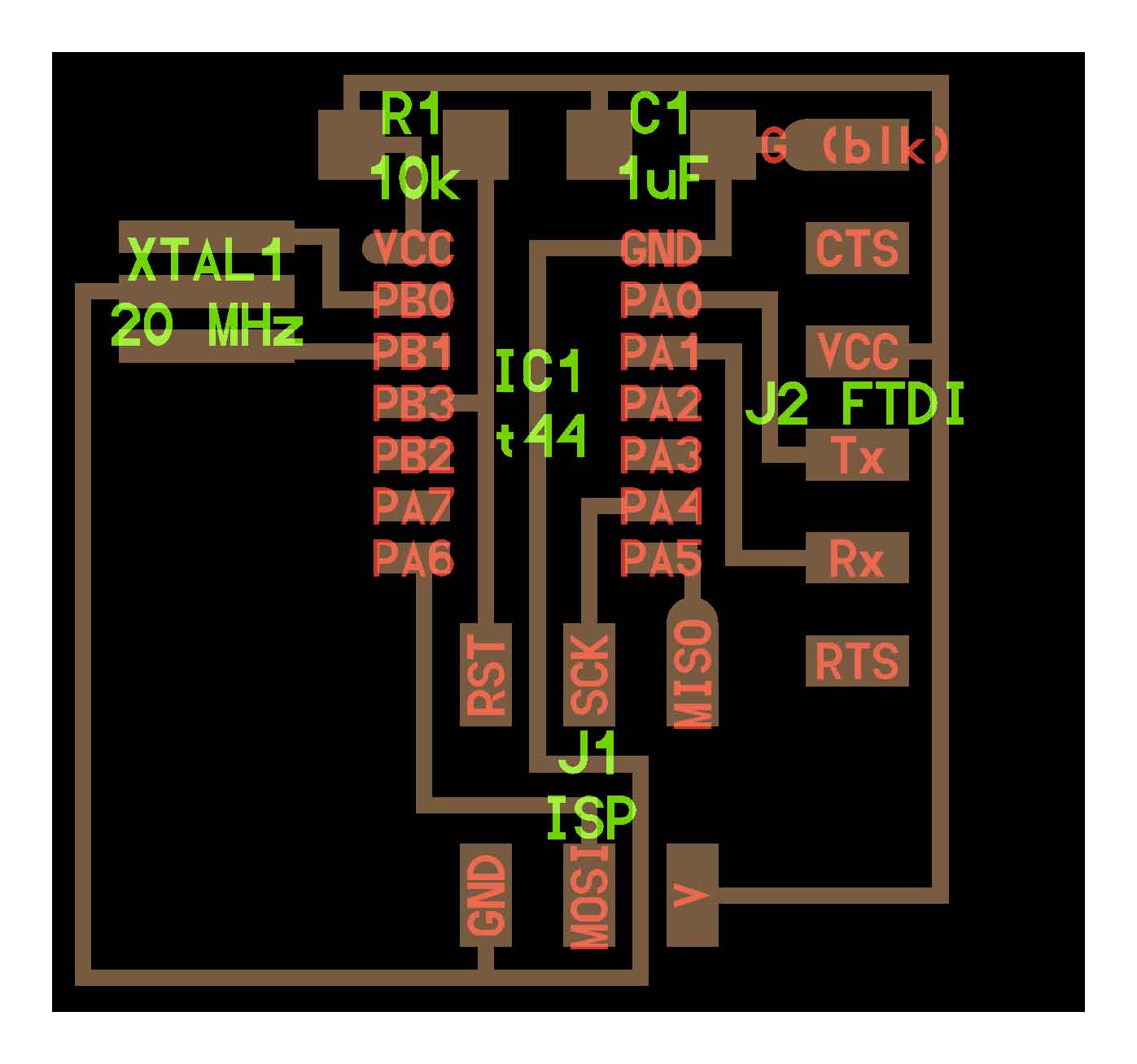
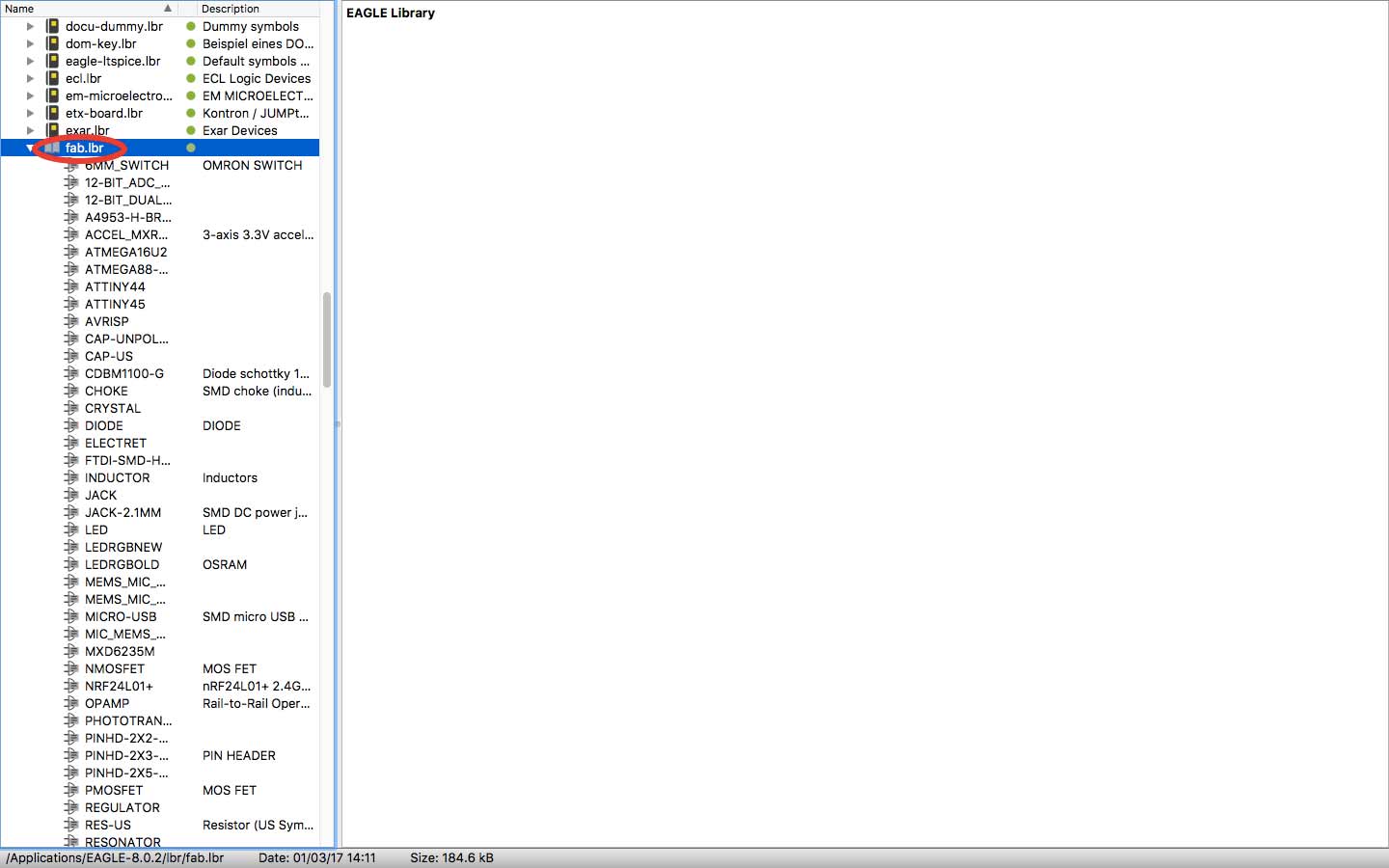
adding at least two components (button and LED with the right current-limiting resistor) and then make it. I decided to use Eagle. I have never used this kind of software before, so I have looking for some tutorial. I found this one very usefull (link here). The first thing that I had to do was installing the fab library (you can find it at bottom of page), which contain all the components for the hello board.
Eagle has two workflow: the Schematic and the Board. The schematic one is the first workflow where I had to work on. I imported all the components ("add" button) necessary from the library. For each components in the library, there are two sketch.
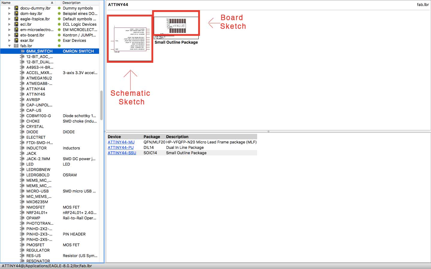
It helps me to understand which is the right components that I have to choose.
Then I linked all components each other following Neil's board, so I added the LED, with resistor (The resistor required was calculated using the specification of the LED and LED calculator.), and the button. To understand how connect the button in the right way, I've read the datasheet.
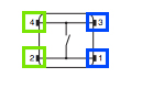
You must connect two pins as you can see in the picture: the greens or the blue ones.
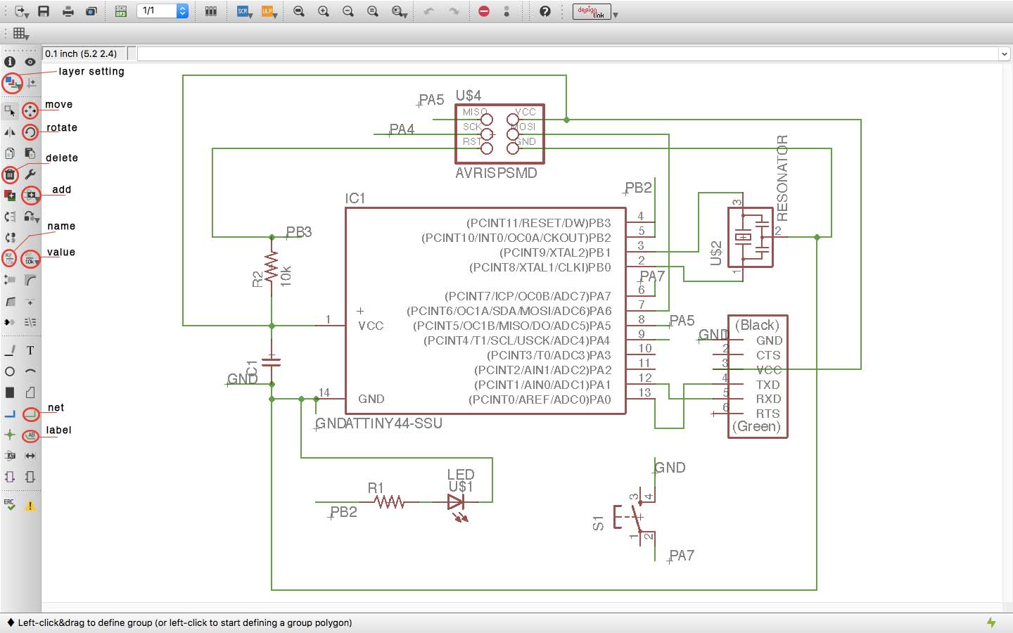
This is my schematic project. I have labelled some components for make my sketch little less chaotic. In the image above I have underlined the main command that I have used. Then I went to File -> Switch to board. It was only at this stage that I realised that the layout in the schematic is not quite as important. In the Schematic workflow I made only the connection between components.
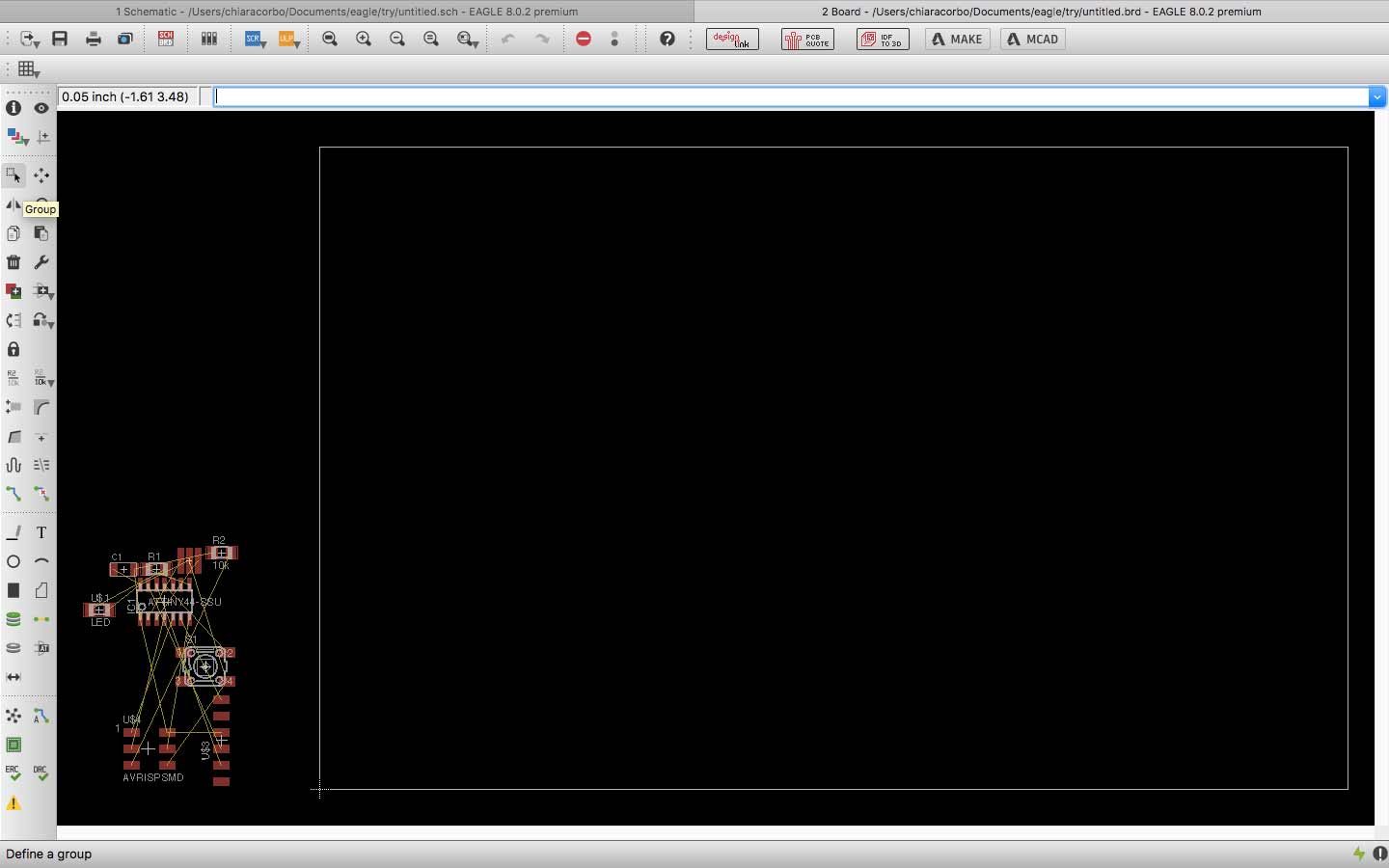
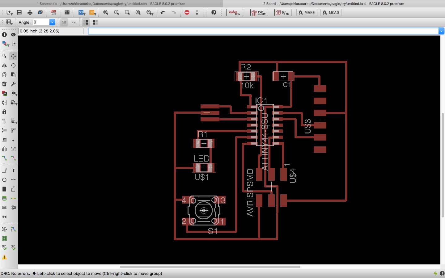
I have moved all components on workflow and I started drawing traces following the yellow lines. At the beginning was a mess understand which were the right connections, so I followed the original sketch to redraw my Hello board.
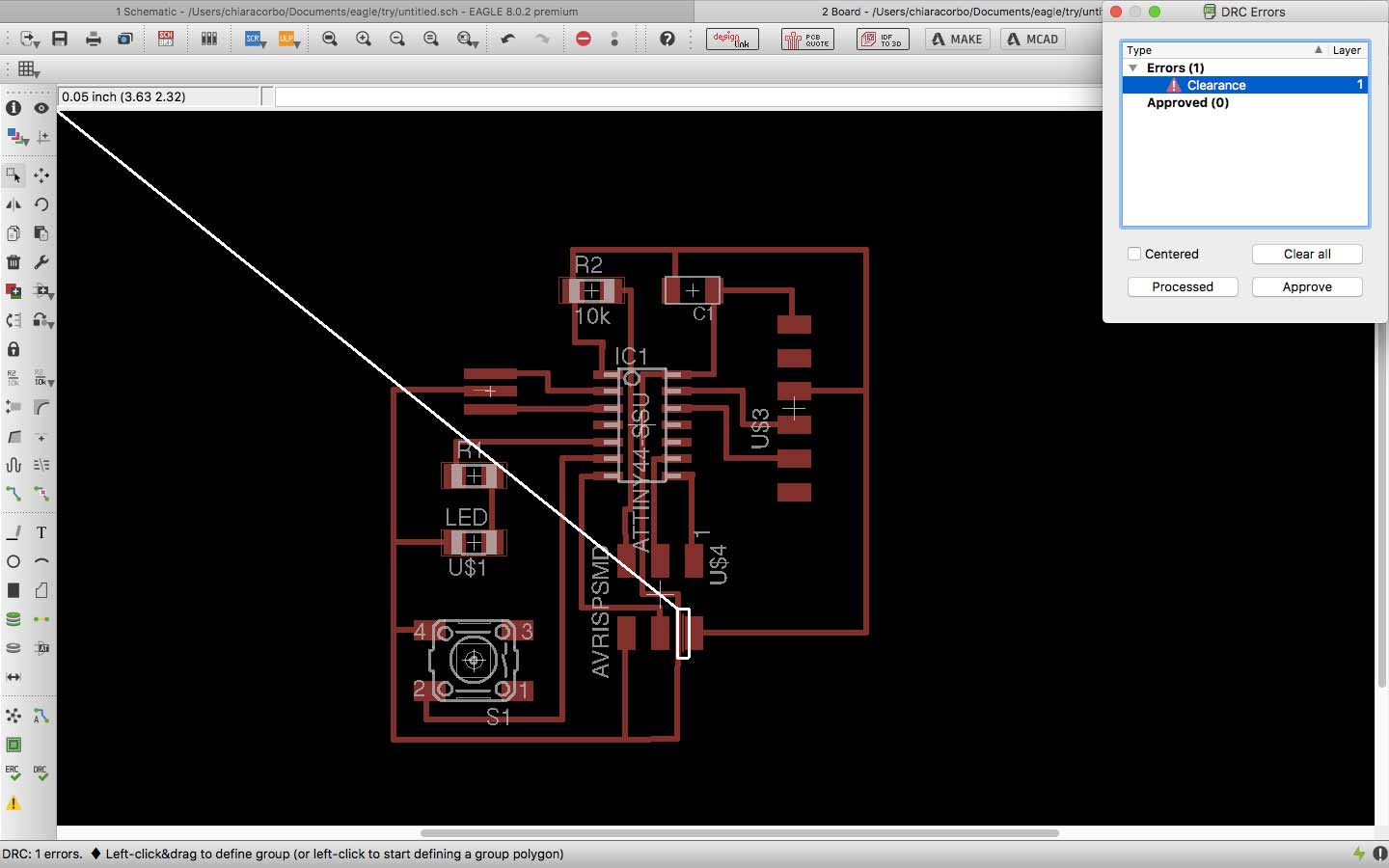
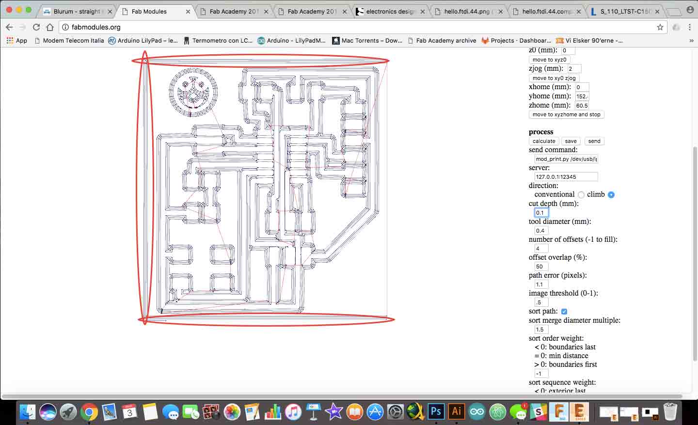
Before exporting the png file, I have redefined and checked the Design Rules(DRC) in Tools -> DRC menu. I have setted appropriate routes characteristics for the endmill that I will use: Clearance (defines the minimum clearance values between objects in signal layers.) and Sizes (Defines the minimum width of any objects in signal layers and the minimum drill diameter). So these are my values:
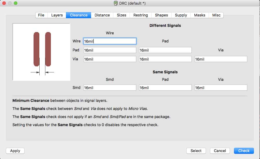
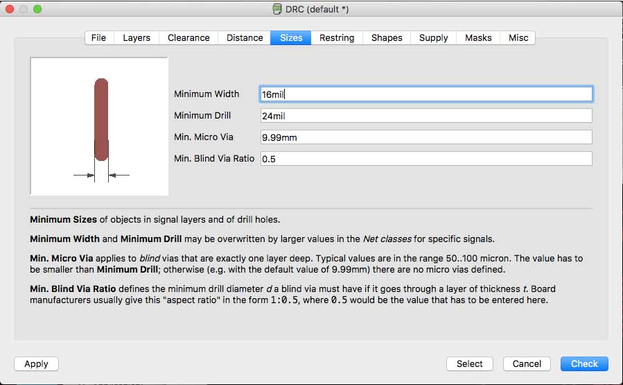
I have founded only a Clearence error. So I have fixed it.
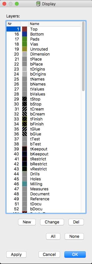
Then I have exported the traces by selecting only Trace level.
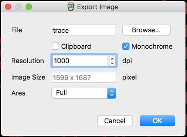
I have saved my file setting this values:
At this point I have exported the file on Gimp and I have followed this steps to create the outline and traces file:
- Image -> Autocrop
- Set canvas size by adding 100px (or more) for each dimension
- New Layer (black) -> moving it below
- New Layer (white) -> moving it above
- Select all -> Shrink (20px)
- Select all -> Invert -> Fill the board with black color.
- Hide white layer and export ETCHING
- Hide trace layer and export CUT
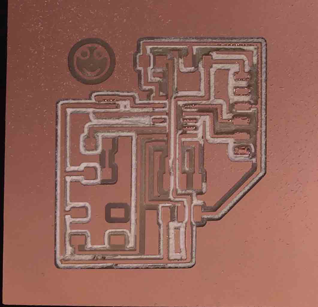
FIRST ATTEMPT
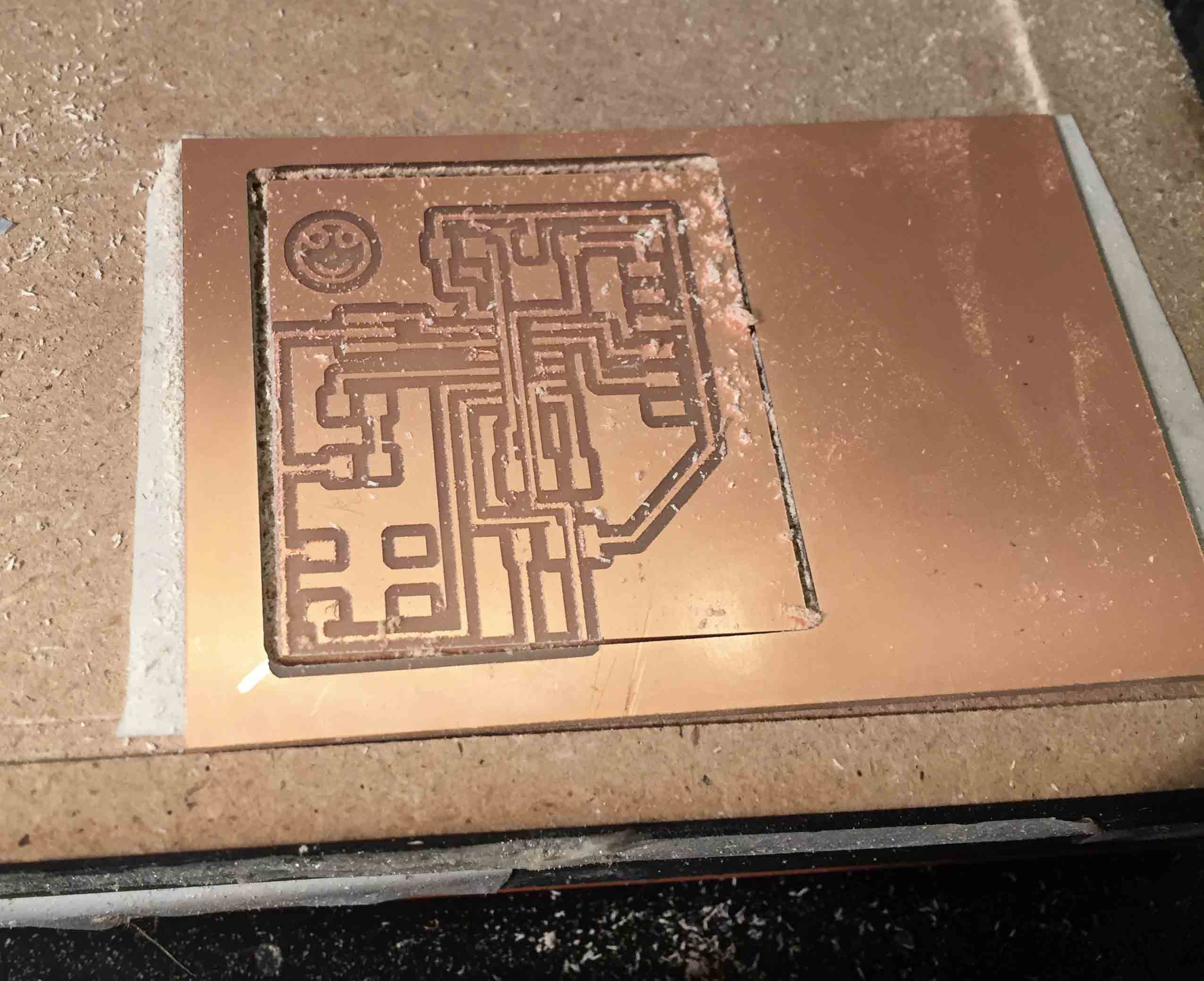
As you can see from the picture, the milling wasn't fine and tip for the outline cut destoied some traces. In this case the problem was in my outline file. I haven't resize it correctly and I changed the tip because that was old.
SECOND ATTEMPT
This time the traces were always imperfect and the cut was to deep. I have stopped the mill for don't break the tip. I have checked the Fabmodules file, but the value was right. I thought that the problem was in the exported file. So I have exported again the trace from Eagle and I have created the outline with Photoshop this time. The latest version of Photoshop doesn't allowed me to work on the exported Eagle file, so I have created a new documents with adding 100px for each dimension.
Then I selected the orginal sketch and I have copied it in the new document. At this point I have followed the same steps that I have used with Gimp. I opened the new files with the Fabmodules for creating the new mill files.
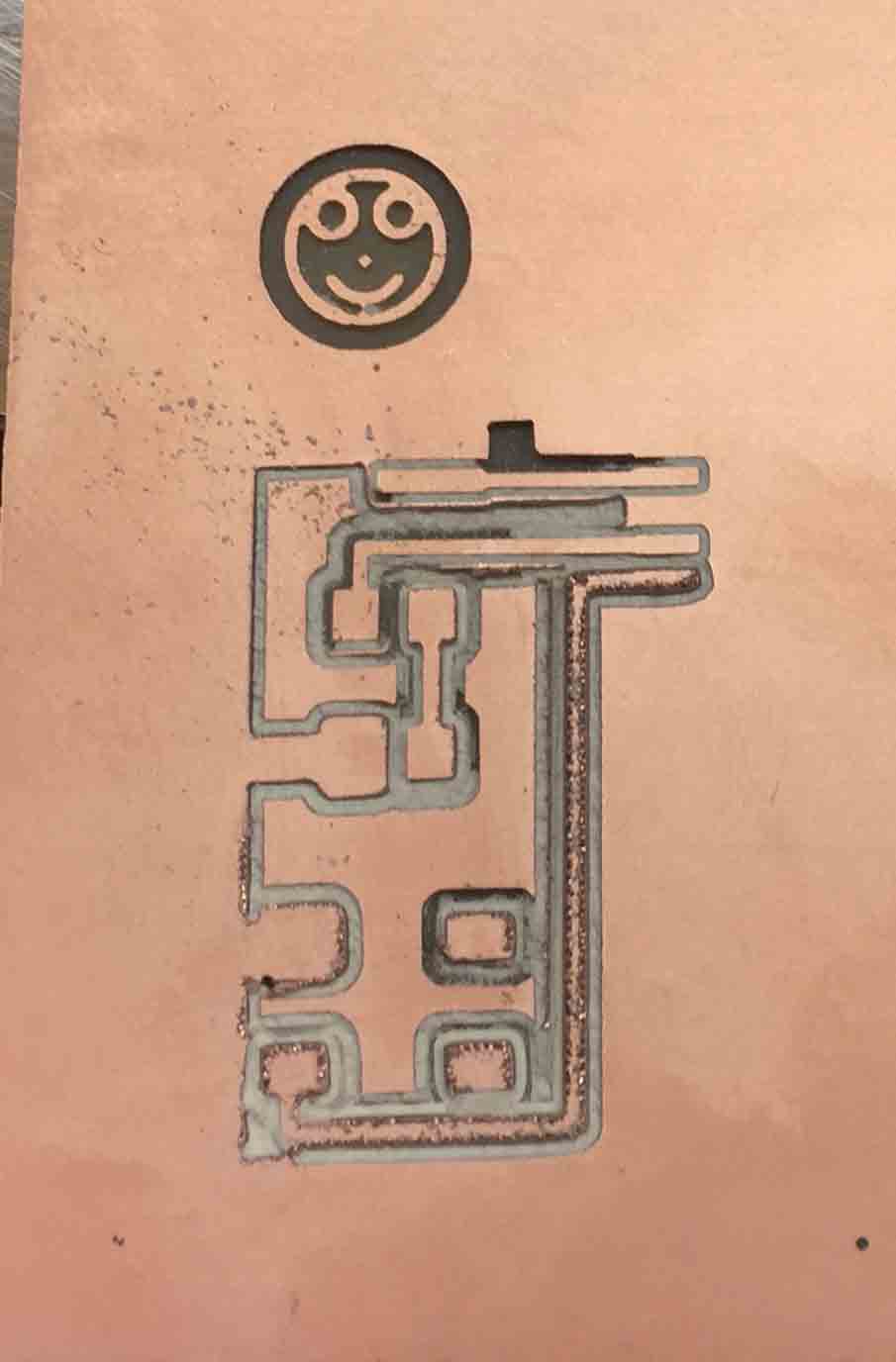
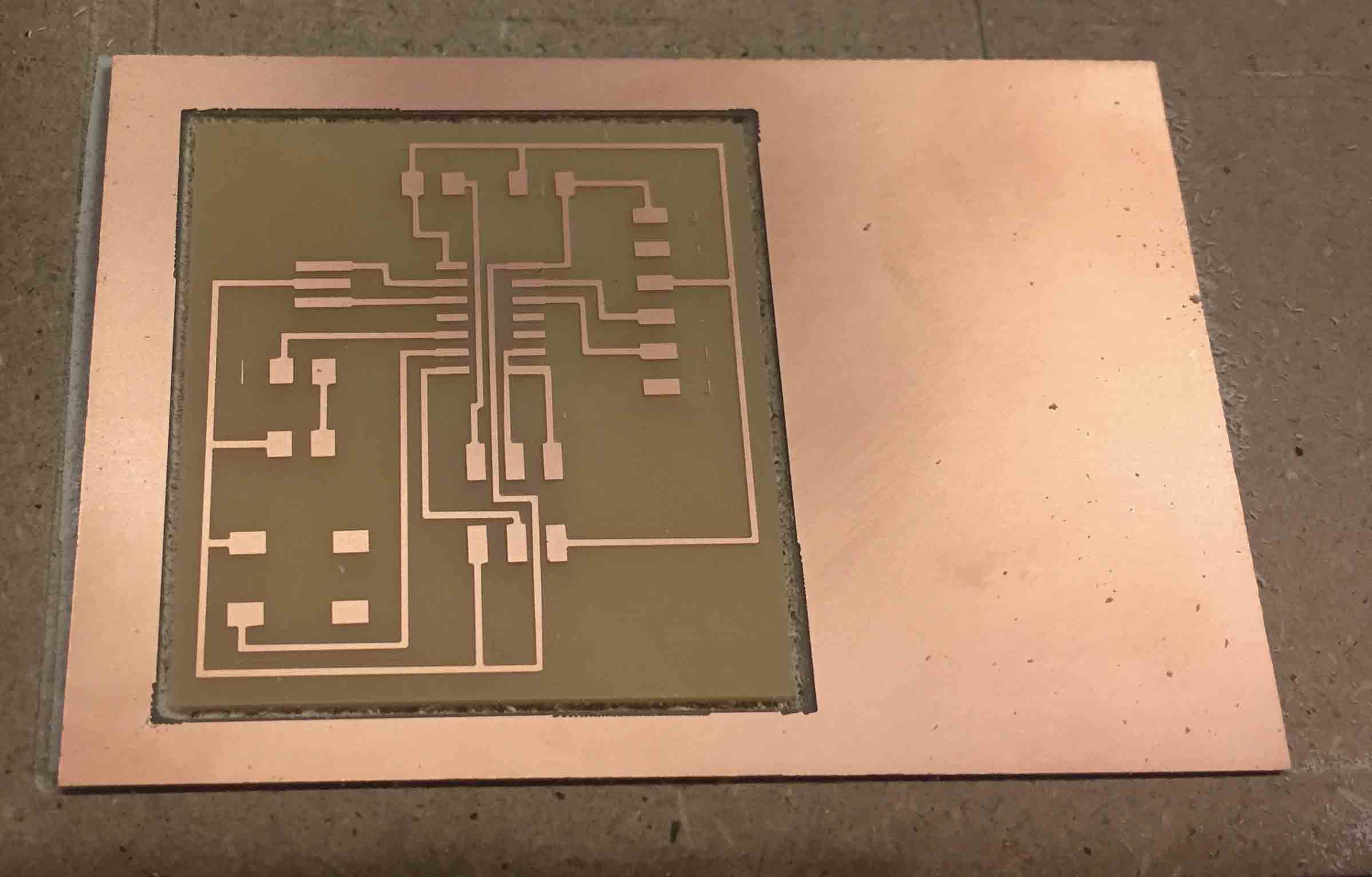
THIRD ATTEMPT
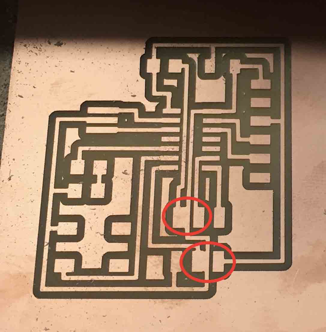
As you can see also this attempt was a disaster. I have stopped again the milling because the board was fixed badly and I had always the problem with the deep cut. I have checked again my files and the value was all correct, but I have found another mistake.
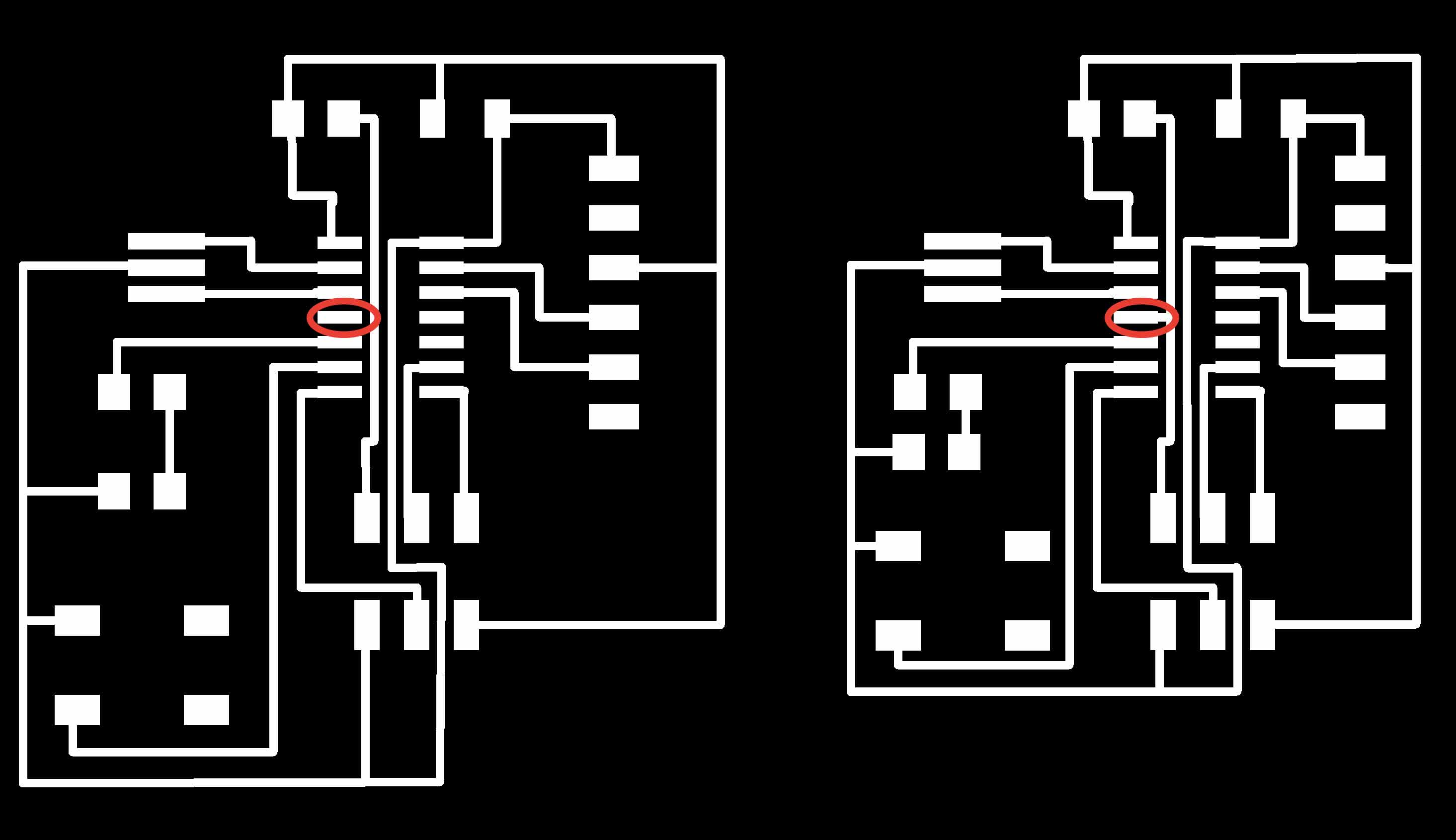
In the image above I have underline the wrong parts. These are some residual trace on Eagle workflow. So I have cut off it by using Photoshop and I have redraw the outline file and then I have recreated the rml file with the Fabmodules.
FORTH ATTEMPT
Also this time I had the same problem with the cut deep. My instructor helps me to understand where was the problem. I tried to use the New Fabmodules to generate the rml files, but we didn’t find the problem yet. So I have tried to do a very simple thing.

I have turning off and on the computer and the Roland, then I have changed the USB cable to connect each other. I have tried to mill it again and finally the board was ready.
I have soldered my board and then I have tested it and it works.
PROGRAMMING
I wanted to try to program it. I used my FabISP for doing it. First of all i've downloaded the hello.ftdi.44.echo.c and hello.ftdi.44.echo.c.make files to program the hello board. For doing it I have followed this tutorial. Suddenly i got this error message.
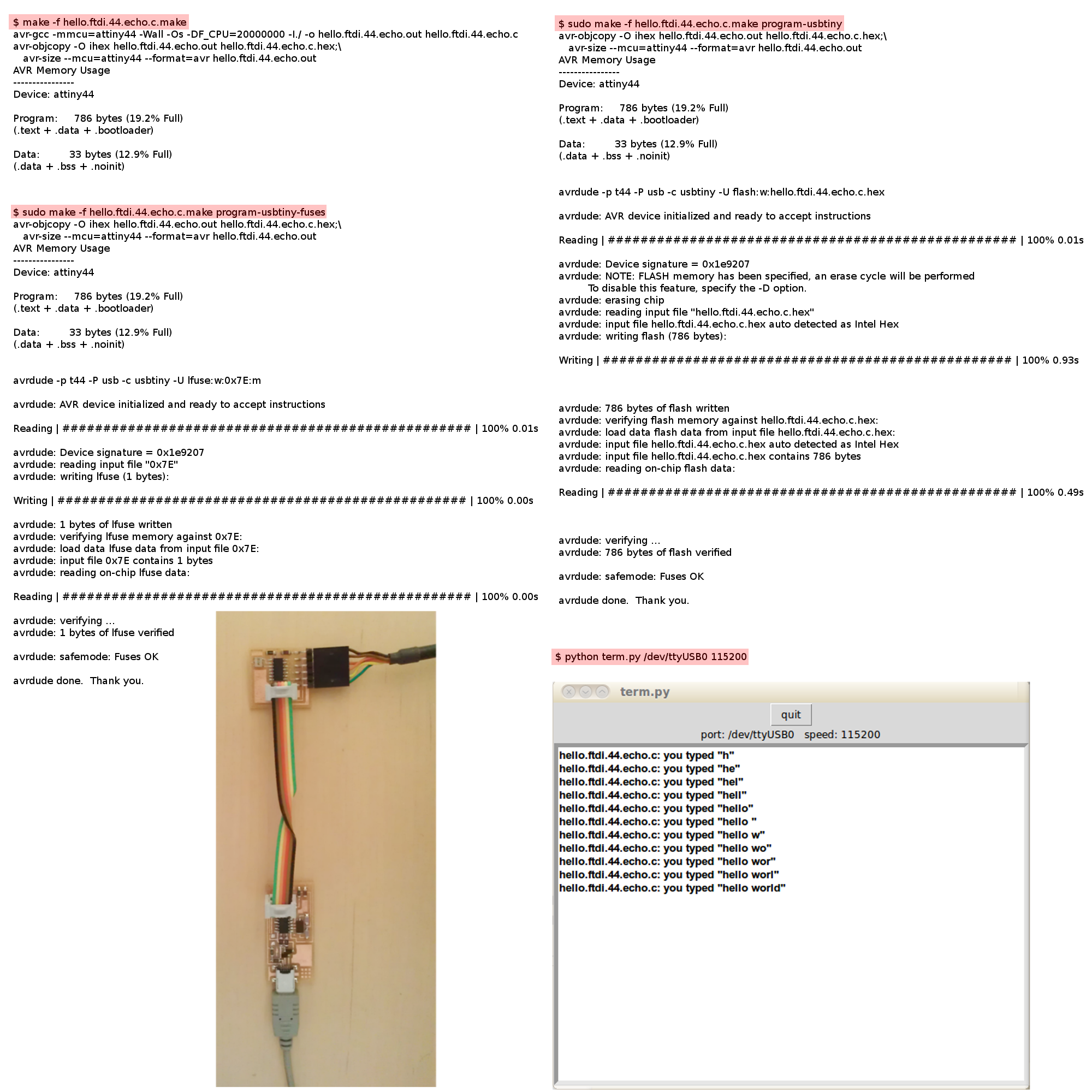
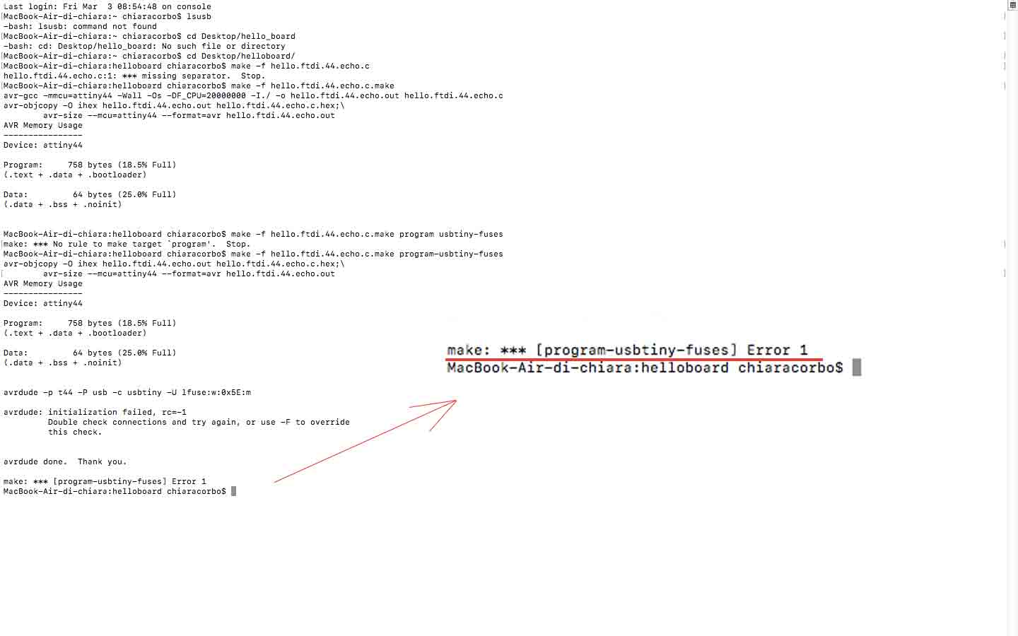
This means that some solder on my boards was weak, so I have checked and fixed it. The resonator on my hello board probably was damaged because I have bourned it during solder procedure. So I have removed it, but for doing it, I have broken some traces.
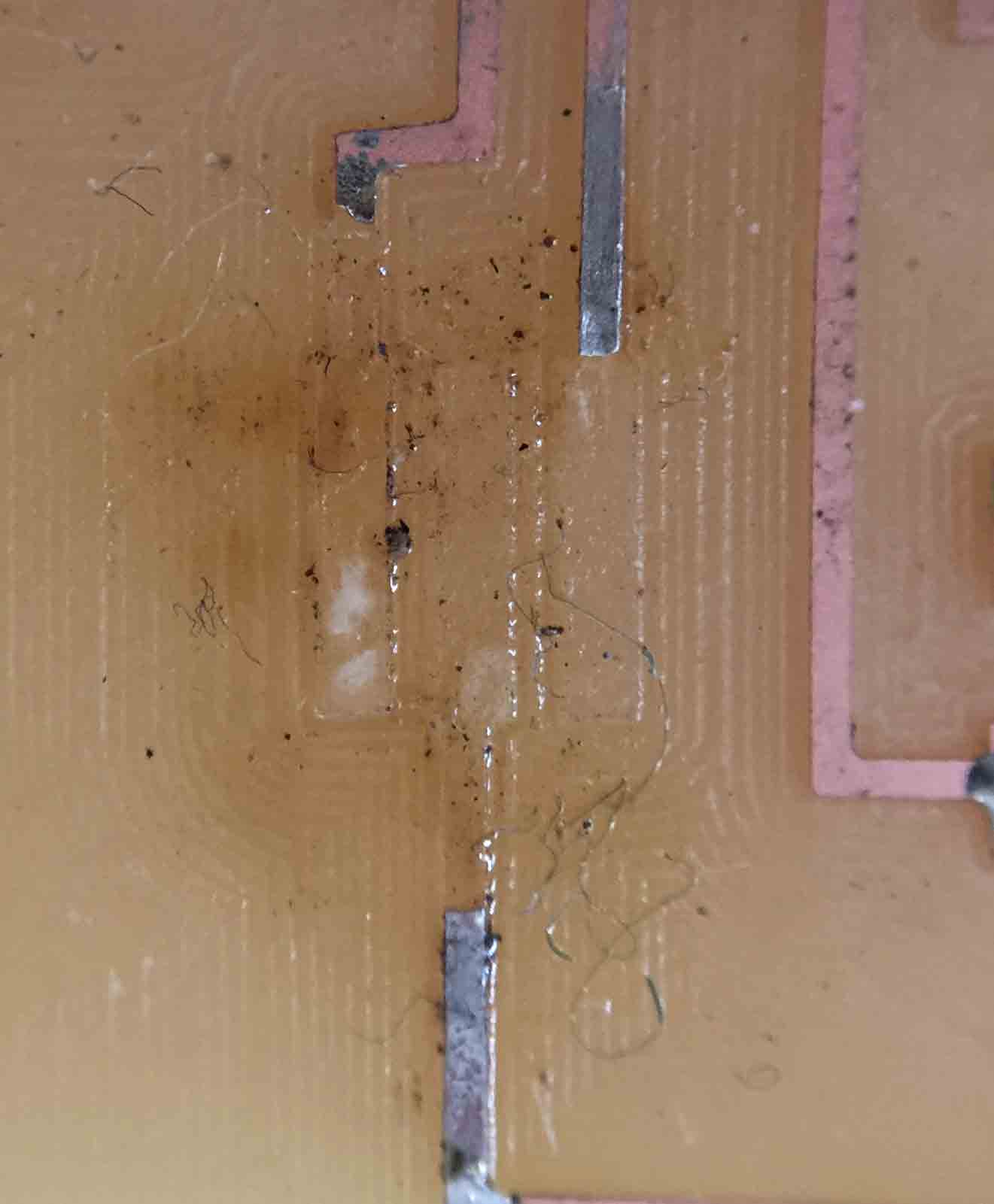
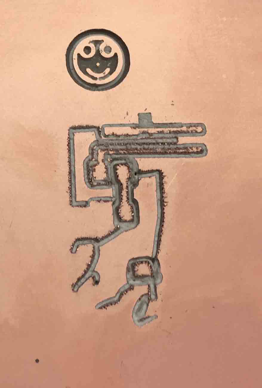
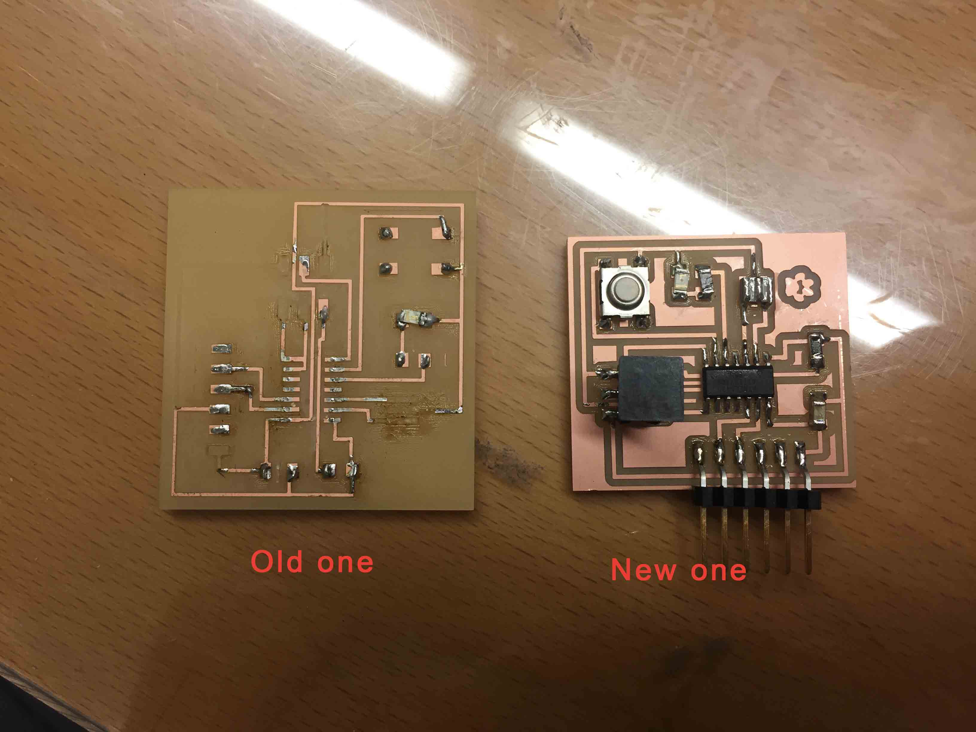
I have tried to fix it but it was impossible, so I had to mill my board again. My first board was to big, so I have decided to modify the traces by optimising the space. I followed the same process of before for creating my outline file with Gimp, but I have a problem with the outline. It was so close to some traces and I have cutted it.
This time I knew the problem. I have done a mistake with the outline colors. I have switched black and white parts, so it cut to close the traces. I have exported (again!) the traces from Eagle and then I have mill it (again!) but...
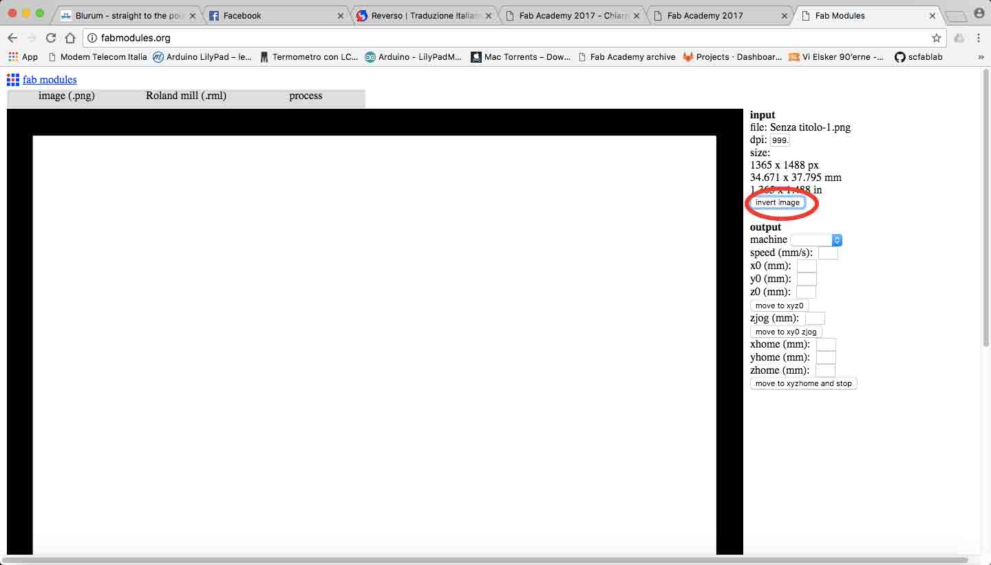
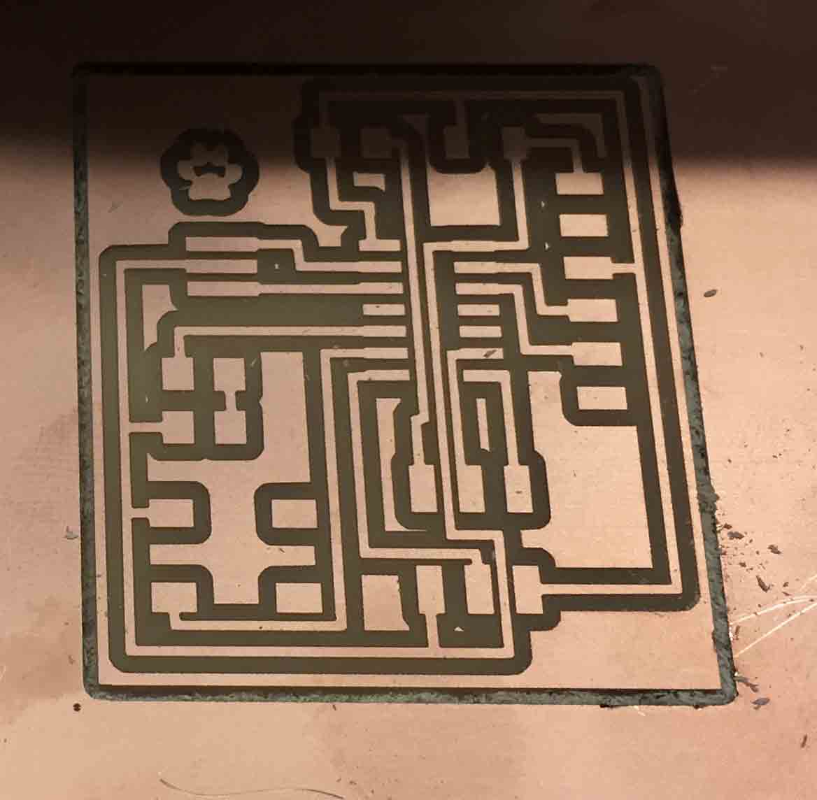
In a rush I didn't checked if I had errors in the design rules and in the Fabmodules I didn't notice that two traces was to close each other and the mill couldn't cut. So I have modify my Eagle's file, I have created new outline file with Photoshop and then I have created rml files with Fabmodules. This time for the outline file, I have clicked on Invert Image command for switch black and white parts.
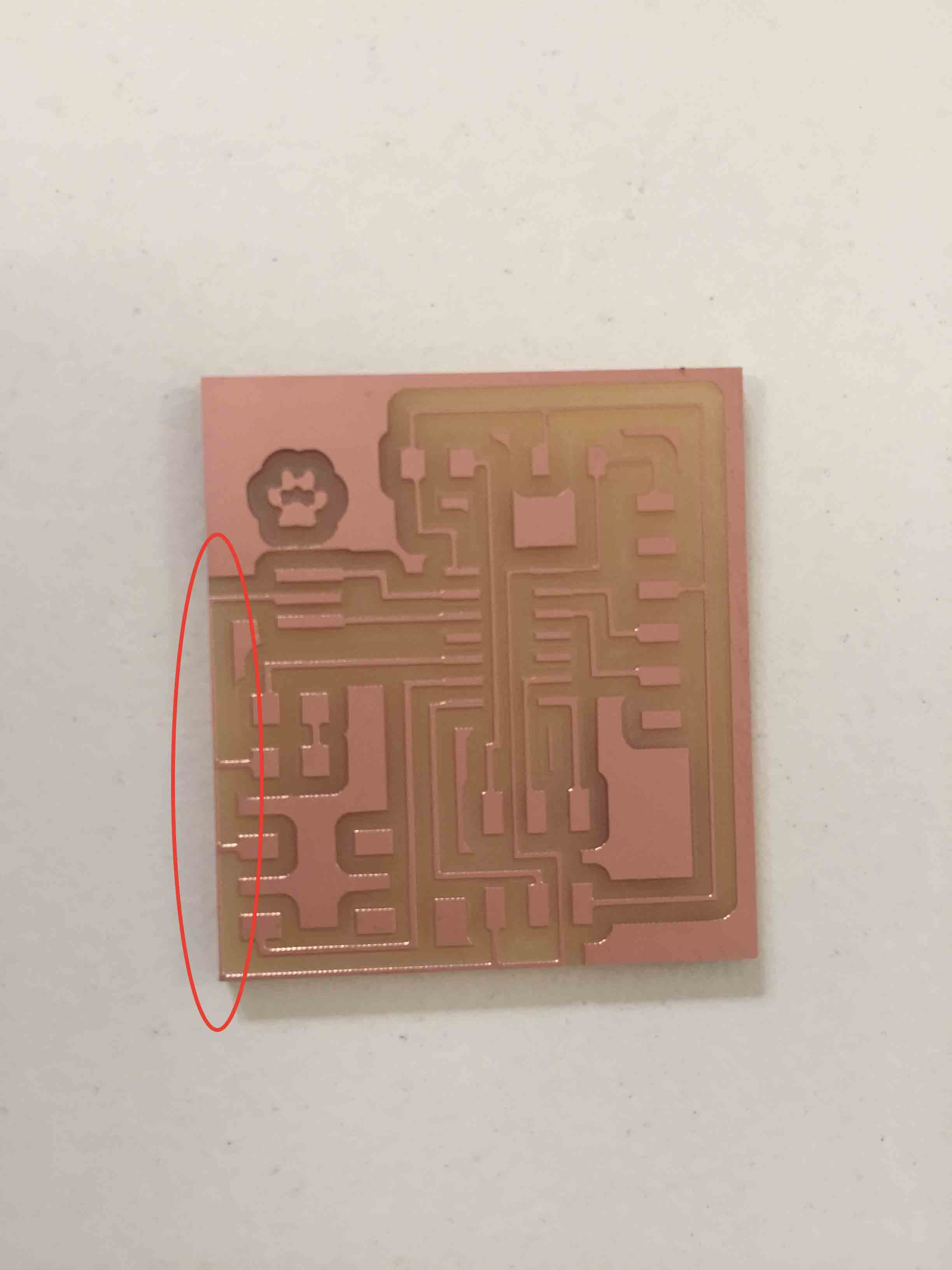
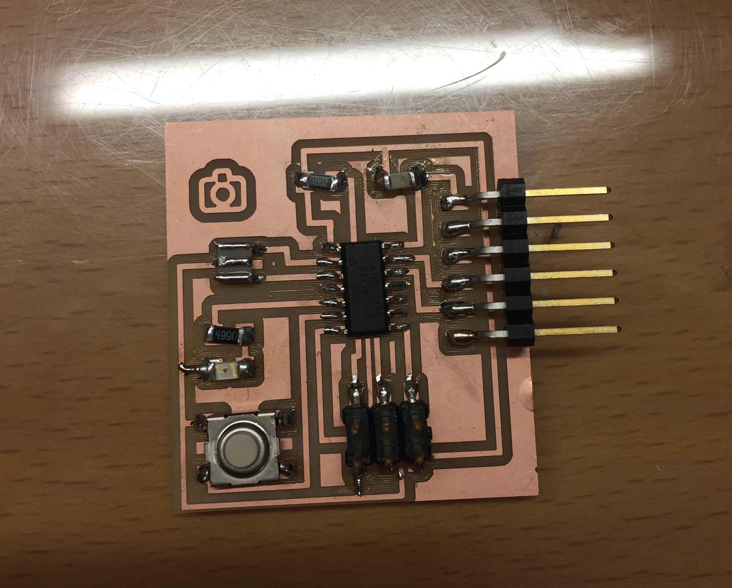
Finally I got my final board!
For don't waste components, I have remove it from the first board and I have soldered it on the new board. This is the result!
I have tested it, I have tried to programm it but I had some problems. Everytime I had always the same message: "Double Check Connection". It means that I have some soldering problem, so I have done a complete check-up.
I haven't found problem, so I have done the same things at my FabISP, but nothing, everything works correctly...so...where is the problem??
UPDATE WEEK 6 - ELECTRONICS DESIGN
I have tried to program my hello board with Neil’s files, but I couldn’t. I always receive this error:
avrdude: initialization failed, rc=-1

               Double check connections and try again, or use -F to override

               this check.
So I checked all my board (FabISP and Hello Board) to understand where was the problem. I have changed some components because they seemed burnt. But my board didn’t work again. I have tried to change the USB cable, but nothing. I’ve looking for some hint on Internet, but nothing. At the end I have thought to start at the beginning. I have checked my original sketch on Eagle and I have found the problem. I hadn’t draw a trace.
So I have fix the board’s sketch on Eagle and then I have milled it again. I have soldered all components on it and finally I have programming it.
CONCLUSION AND DOWNLOAD
You can find all files here

This work is licensed under aCreative Commons Attribution - ShareAlike 4.0 International License.