Week 15
Networking and Communications
Objectives
Learning Outcomes
Have I ...
Documentation
For this assignment, I read this page, to urdestand RS-232, RS-422, RS-485 in order to learn more. Then, I design my networking boards, node and bridge, using eagle. After that, I milling both boards, 1 bridge and 2 nodes. Inmediately, electronic components were welded. As a result, boards are ready to be programmed.
Electronic hardware
I start doing my own design of this boards. For this I did reverse engineering to obtain the schematic.
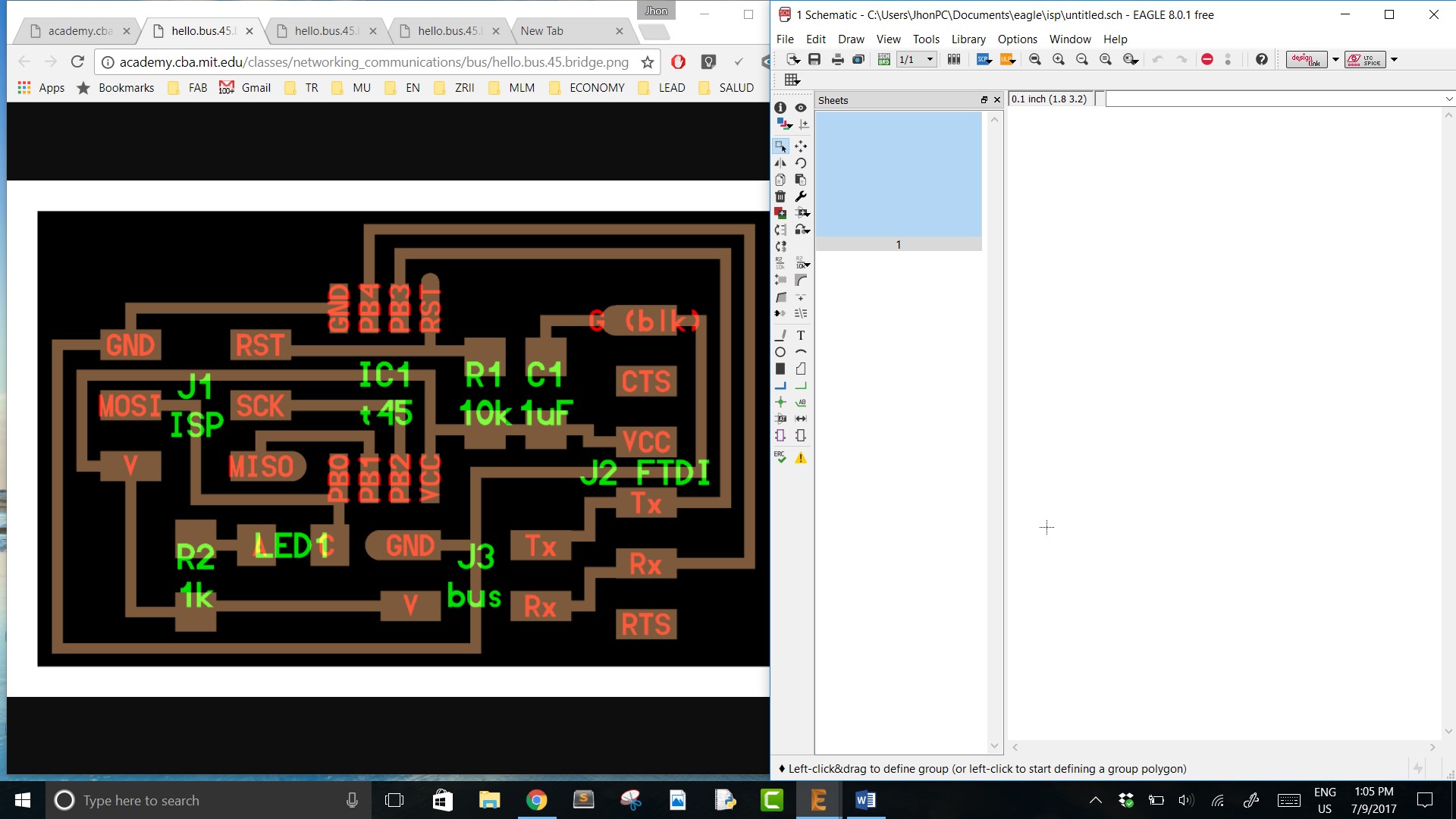
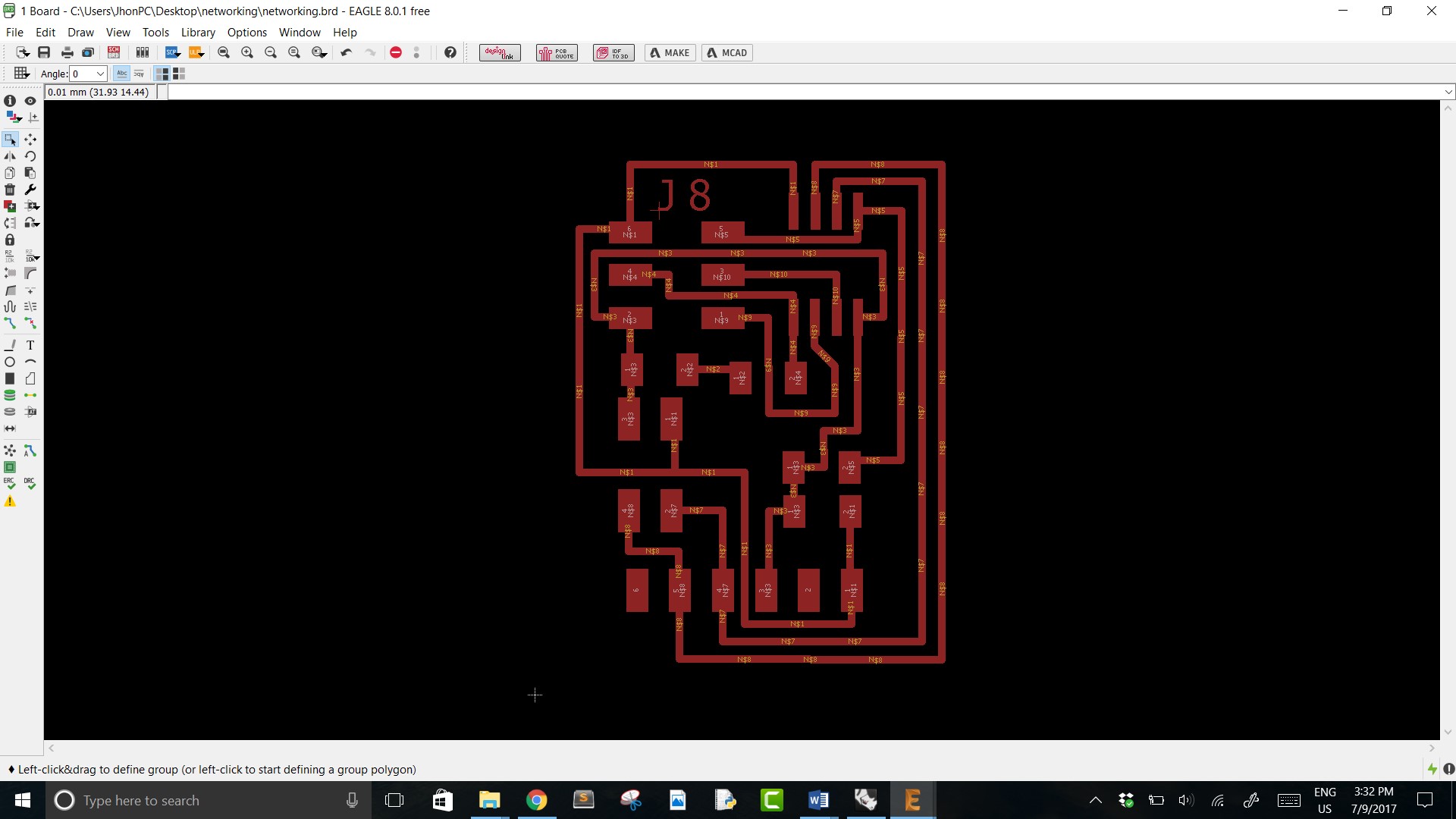
Using "Add" tool of Eagle add the components. Always try to maintain a good layout and order to later make the connections without much difficulty.
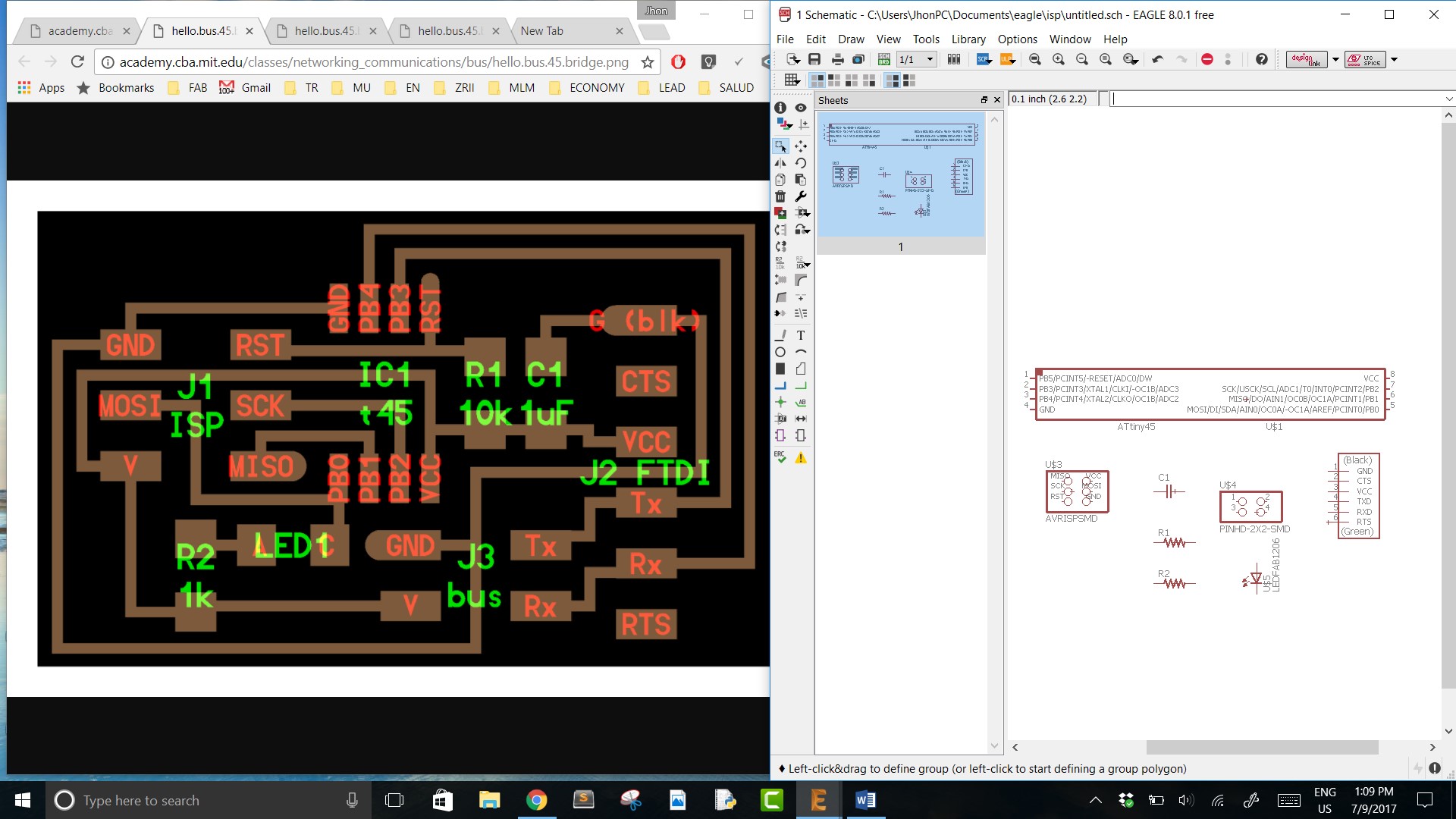
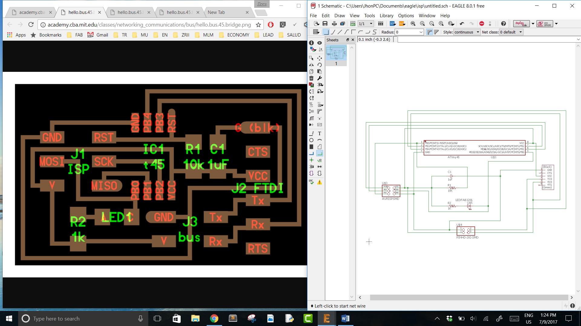
When you finish placing the components. Use "Net" tool to do connections. Use the "Junction" tool at intersections to make sure they are really joined. This as long as it is required. Once finished this process, click on "Genete/switch to board" and "Yes". The window that has appeared has components and yellow lines that means connections.
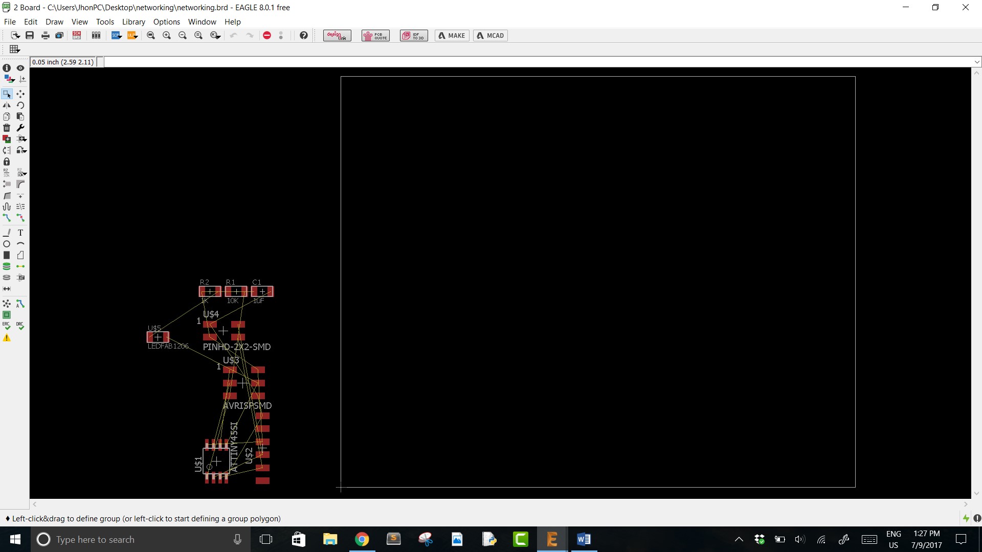
Now, using "Move" let to order pieces inside white line, which represents the work area and the size of our board.
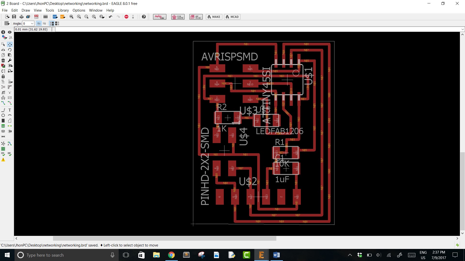
Finally, I add a special symbol, "J8". To export ".png", write "exp" on command tool bar. In this new window, let's to select a file to save our image, click on "Monochrome", "2400" dpi, area "Full" and click on "OK".
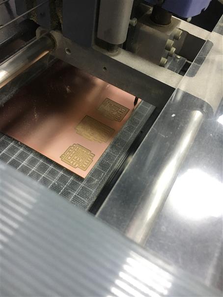
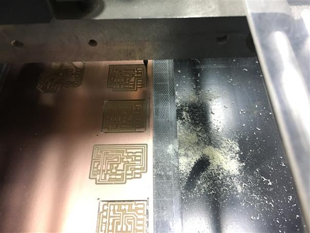
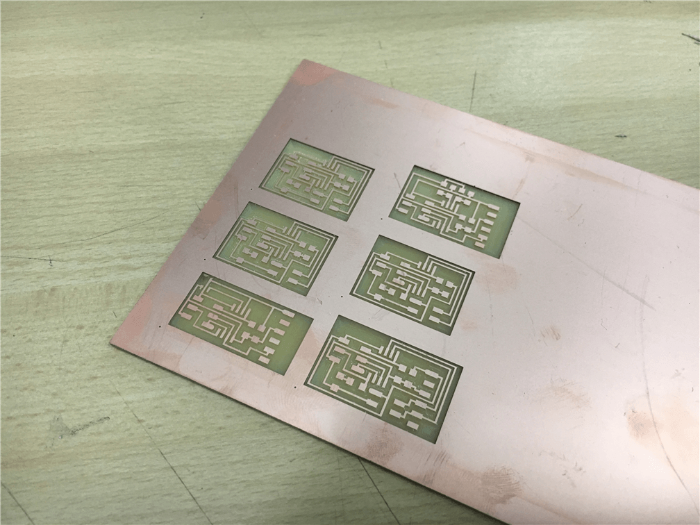
Using Modela MDX-20 goint to mill on copper PC board. Open FabModules, load .png (files are at end), choose 1/64" milling tool, "4" value at "offsets" and "0.1" at "error"(rest remains as it is). Now, set your Zero to start. Click on send it!
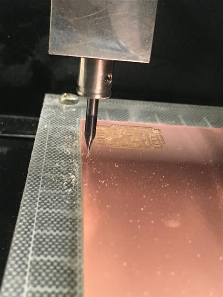
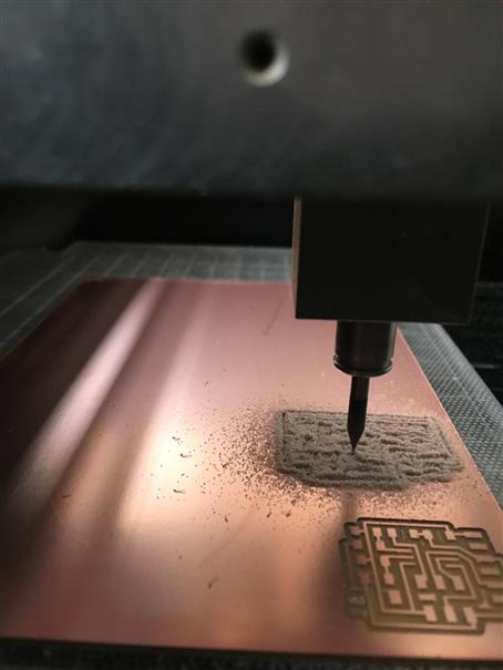
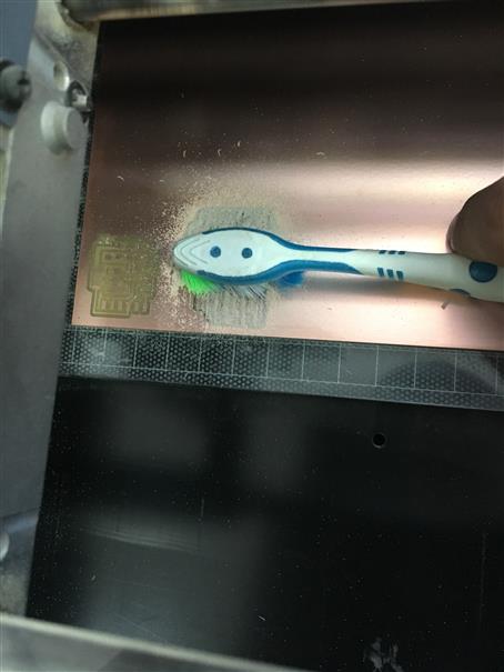
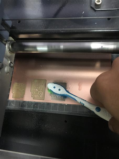
Using a toothbrush can remove the chip.
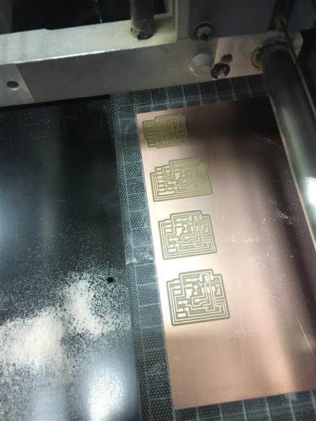
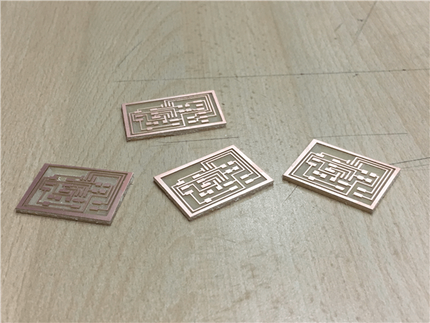
In order to use the whole copper PCB possible, we are going to use 1/64" milling tool for circuits and 1/32" to cut borders. So, you have to take notes the "xmin, ymin" for each board. Then, when circuits are milling, let's to change tool by 1/32", load a file, DON'T FORGET TO MOVE THE HEAD TO POSITION YOU TAKE NOTE, click on send it!
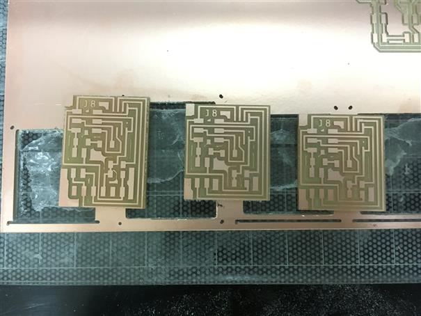
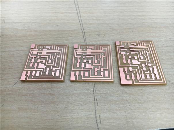
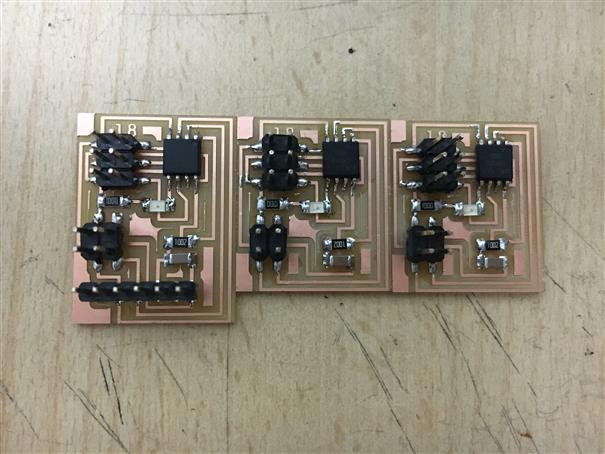
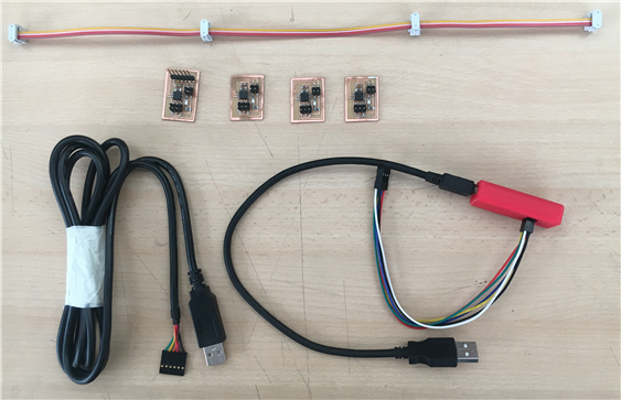
Boards are ready to be welded (2 nodes - 1 bridges)
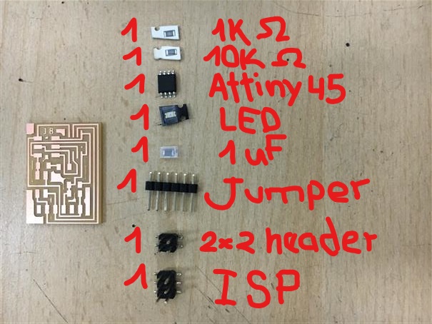
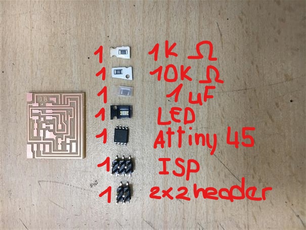
Look for electronic components.
Boards are ready!
NEIL's BOARD
In order to use adequately bakelite card, it is preferable milling one after another as I did. Then, using a guillotine or interior files (hello.bus.45.bridge // hello.bus.45.node) can cut the border. Next, proceed to weld as other taks.
Then, make your connection cable using multicolor ribbon cable and FCI cheaders 2x2 or 2x3. To complete the list of tools and materials have your cable FTDI and FabISP on hand.
Programming boards
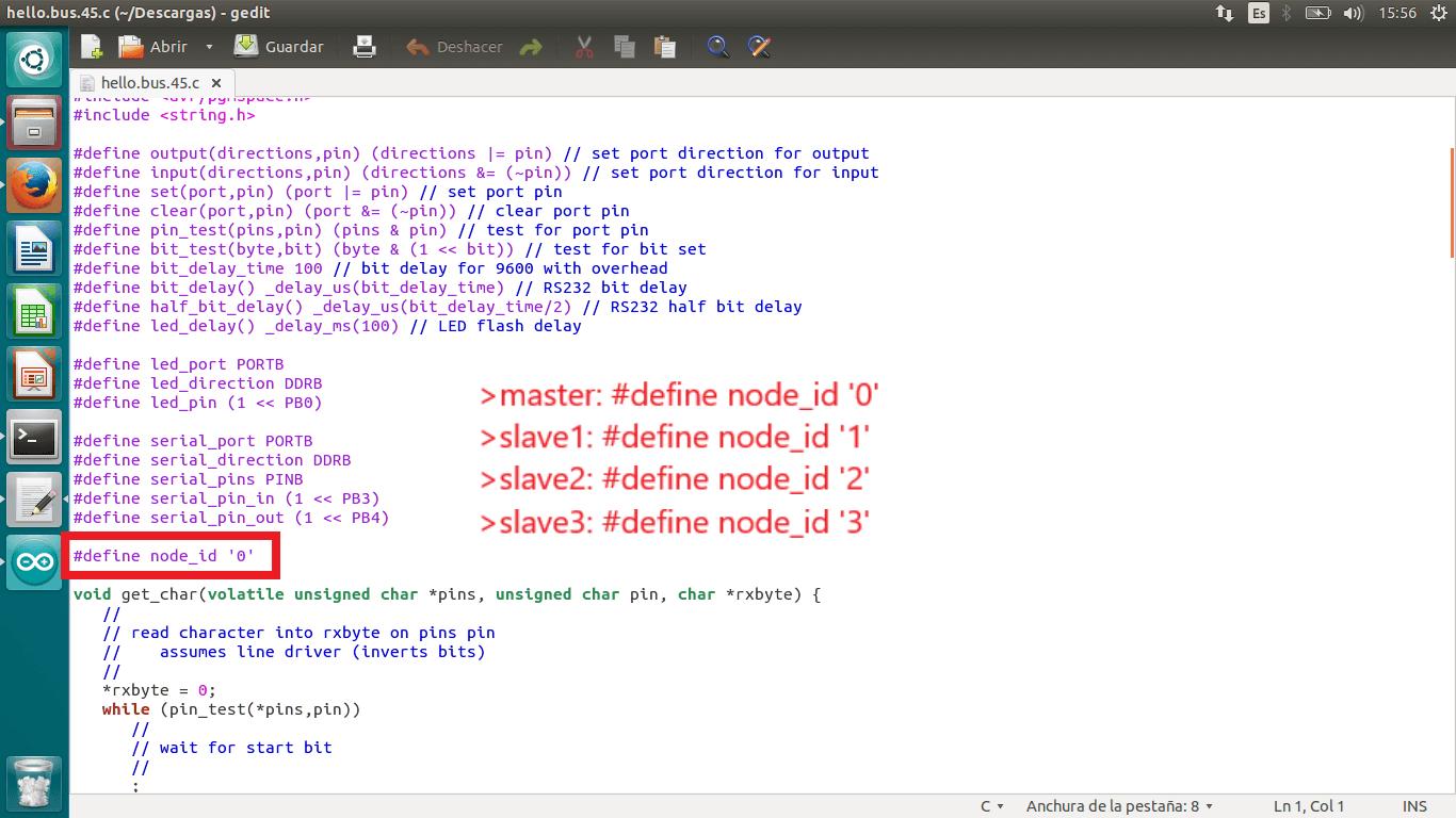
First, download those files hello.bus.45.c and hello.bus.45.make. Second, it is necessary to change a code line in file .c in accordance with the board that is being programmed at the moment.
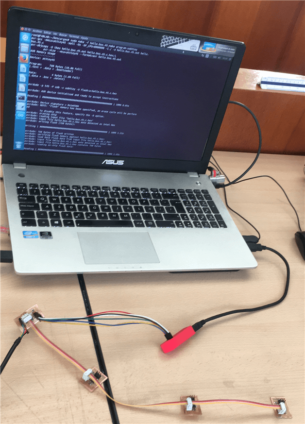
To programm the boards, can be programmed one by one or all together connected, as I did. Where the FabISP is connected is the selected.
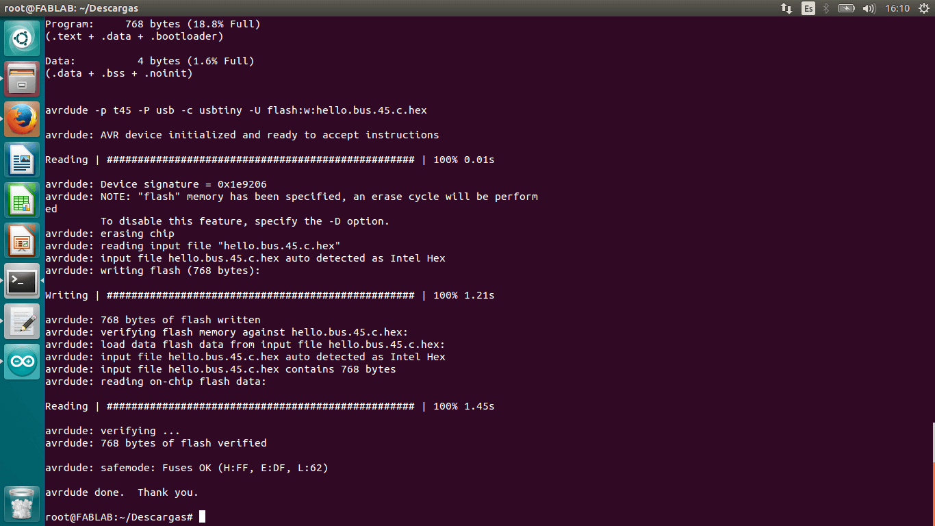
Finally, open terminal, enter to folder where files makefile and .c are, copy the line below and press enter:
sudo make -f hello.bus.45.make program-usbtiny
Files
Result
After all, open arduino serial window, write numbers and see how leds blink.