
ABOUT EAGLE
EAGLE (Easily Applicable Graphical Layout Editor) is a flexible and expandable EDA schematic capture, PCB layout, autorouter and CAM program. EAGLE is popular among hobbyists because of its freeware license and rich availability of component libraries on the web.
Get Eagle Here: http://www.cadsoftusa.com/downloads
ASSIGNMENT
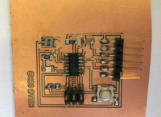
1. Add a button and LED to the echo hello-world board
2. Check Design Rules and Make the Echo hello- world board work

After the Installation, I learnt that in Eagle PCB designing has two step process, first process is to design the schematic, then to lay out a PCB based on that schematic. EAGLE’s board and schematic editors work hand-in-hand. A well-designed schematic is critical to the overall PCB design process. It will help you catch errors before the board is fabricated, and it’ll help you debug a board when something doesn’t work.
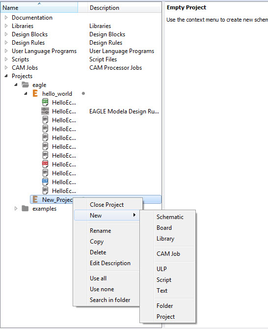
I started by making a new project folder for the hello echo board design. In the control panel, under the “Projects” tree, right click on the directory where you will bring the project to live (by default EAGLE creates an “eagle” directory in your home folder), and select “New Project”.
I also learnt that the folder created for the project are like our computer folders
including an EPF link, On exploring the link I realised that it has a link where all files of the project created were stored together the schematic and board drawing together.
To start with the project, I added the fab.lbr into my computer C drive>
program files > Eagle > Library
To begin the design process, we need to lay out a schematic.
To add a schematic to a project folder, right-click the folder, hover over “New” and select “Schematic”
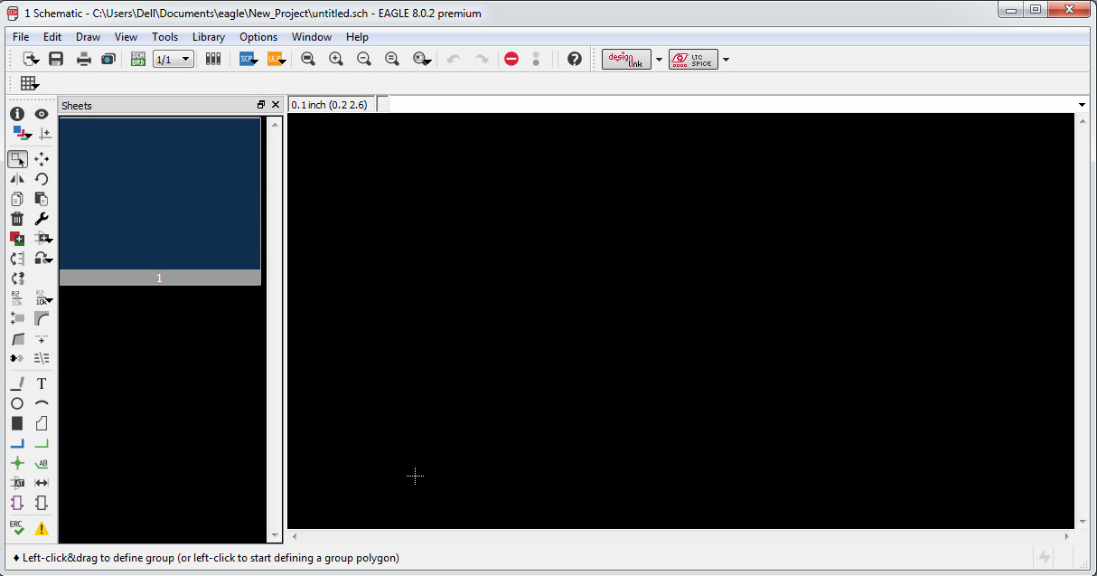
A new Window to layout the schematic opens up separately
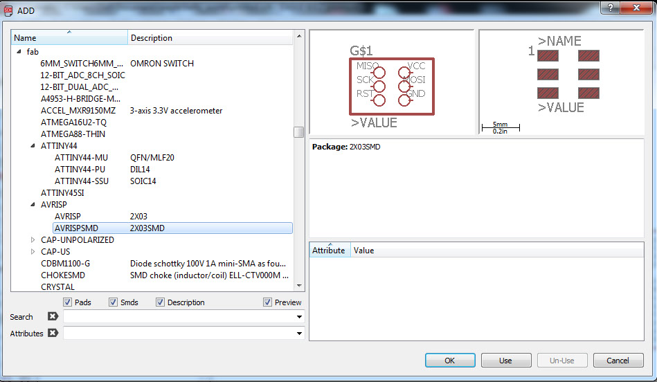
The ADD tool – (on the left toolbar, or under the Edit menu) – is what you’ll use to place every single component on the schematic. The ADD tool opens up a library navigator, where you can expand specific libraries and look at the parts it holds. With a part selected on the left side, the view on the right half should update to show both the schematic symbol of the part and its package.Add components from the fab library to the schematic, add all the components of the circuit required in similar fashion
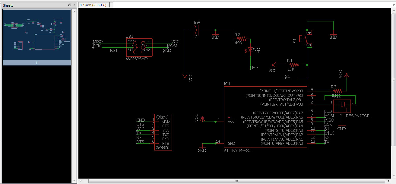
After selecting the components, connect them using net tool and junction tool to connect the components as per the circuit. I learnt to label also understood that the eagle connected pins with same labels
To use the NET tool, hover over the very end of a pin (as close as possible, zoom in if you have to), and left-click once to start a wire. Now a green line should be following your mouse cursor around. To terminate the net, left-click on either another pin or a net.
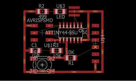
Check whether the board has all the components
Place them such that the connections are made easily by creating convenient tracks or pads
Try to optimize the board size so that it is small
Takes less to mill
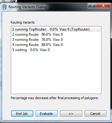
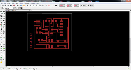
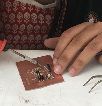
Attempt to auto routing but the connections were extremely confusing so I opted out and decided to learn manual routing techniques in eagle.
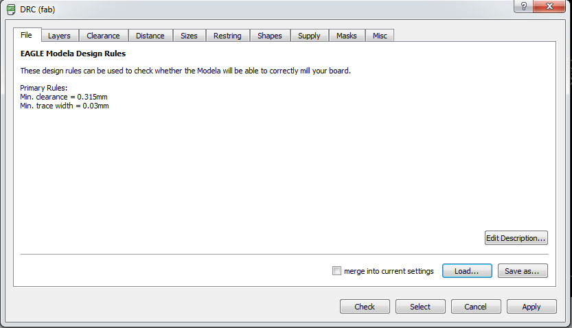
Upon understanding the design basics I went about downloading the fab.dru and add that to Eagle for checking my board designs.
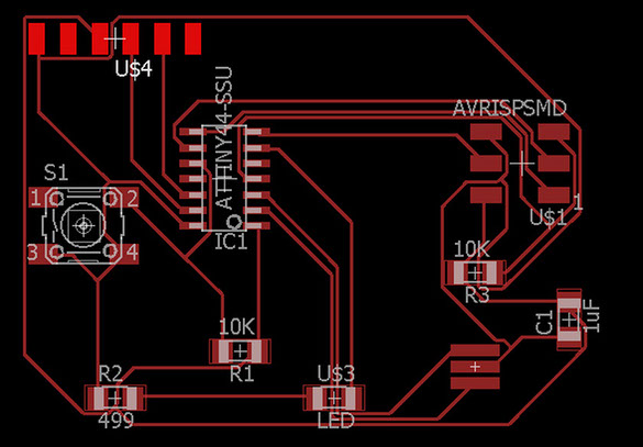
Routing attempts I made to learn and understand the system. Tools used were ratsnet to check the connections of the board. As
soon as the routing was done the yellow lines converted to red. The width of the track started with 0.03 then eventually used 0.01
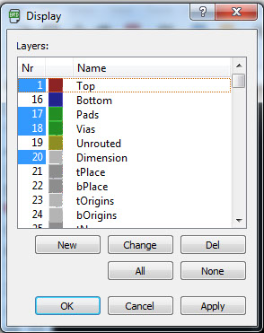
to create the track path. Then Turn off all the layers kept the
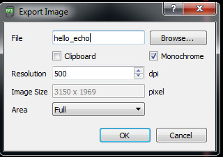
To generate the boards for milling, The files had to be selected in accordance to the operation forming. For milling the board 1/16 milling bit was used and only the top layer was selected and exported as monochrome image with 300 to 400 dpi value.
To cut the board 1/32' milling bit was used the dimension layer or tplace was kept active and a png image which was monochrome and around 300 dpi was generated
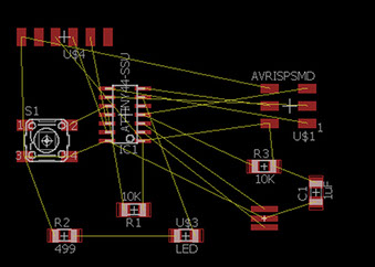
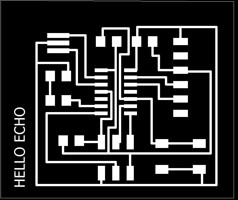
Go to board, where a new window opens up with all the components with some yellow connections which need to connected such that they don't cross or overlap each other. The yellow lines, called airwires, connect between pins and reflect the net connections we made on the schematic. There should also be a faint, light-gray outline of a board dimension to the right of all of the parts.
Important role in this PCB layout will be arranging the parts, and then minimizing the area of our PCB dimension outline. PCB costs are usually related to the board size, so a smaller board is a cheaper board. So use the set of design rules and link the components in that order
Site created by Lavina Utamani using Adobe Muse | fabacademy 2017