Goal of the Assignment
The goal for this week is to work on networking part, which means getting an understanding on how to communicate between boards
In this assignment we will learn how to make a wireless communication between two boards using the NRF24L01 transceiver module.
what is protocol?
protocol is a system of rules that allow two or more entities of a communications system to transmit information via any kind of variation of a physical quantity.
Serial Communication Protocols
Serial communication protocols for data include the RS-232 protocol, which has been used for communication of modems. The MIDI protocol for music and sound applications is also a serial protocol.
Over the years, dozens of serial protocols have been crafted to meet particular needs of embedded systems. USB (universal serial bus), and Ethernet, are a couple of the more well-known computing serial interfaces. Other very common serial interfaces include SPI, I2C, and the serial standard we’re here to talk about today. Each of these serial interfaces can be sorted into one of two groups: synchronous or asynchronous.
A synchronous serial interface always pairs its data line(s) with a clock signal, so all devices on a synchronous serial bus share a common clock. This makes for a more straightforward, often faster serial transfer, but it also requires at least one extra wire between communicating devices. Examples of synchronous interfaces include SPI, and I2C.
Asynchronous means that data is transferred without support from an external clock signal. This transmission method is perfect for minimizing the required wires and I/O pins, but it does mean we need to put some extra effort into reliably transferring and receiving data. The serial protocol we’ll be discussing in this tutorial is the most common form of asynchronous transfers. It is so common, in fact, that when most folks say “serial” they’re talking about this protocol (something you’ll probably notice throughout this tutorial).
The clock-less serial protocol we’ll be discussing in this tutorial is widely used in embedded electronics. If you’re looking to add a GPS module, Bluetooth, XBee’s, serial LCDs, or many other external devices to your project, you’ll probably need to whip out some serial-fu.
SPI
SPI, or Serial to Peripheral Interface, is a very low power, four wire serial communication interface designed for IC controllers and peripherals to communicate with each other.
The SPI bus is a full-duplex bus, which allows communication to flow to and from the master device simultaneously at rates of up to 10Mbps. The high-speed operation of SPI generally limits it from being used to communicate between components on separate PCBs due to the increase in capacitance that longer distance communication adds to the signal lines. PCB capacitance can also limit the length of SPI communication lines.
While SPI is an established protocol, it is not an official standard which leads to several variants and SPI customizations which can lead to compatibility issues. SPI implementations should always be checked between master controllers and slave peripherals to ensure that the combination will not have any unexpected communication problems that will impact the development of a product.
SPI Lines
MISO (Master in Slave out): The MISO line is configured as an input in a master device and as an output in a slave device.
MOSI (Master out Slave in): The MOSI is a line configured as an output in a master device and as an input in a slave device wherein it is used to synchronize the data movement.
SCK (serial clock): This signal is always driven by the master for synchronous data transfer between the master and the slave. It is used to synchronize the data movement both in and out through the MOSI and MISO lines.
SS (Slave Select) and CS (Chip Select): This signal is driven by the master to select individual slaves/Peripheral devices. It is an input line used to select the slave devices.
Master Slave Communication with SPI Serial Bus
Single Master and Single Slave SPI Implementation
Here, the communication is always initiated by the master. The master device first configures the clock frequency which is less than or equal to the maximum frequency that the slave device supports. The master then selects the desired slave for communication by dragging the chip select line (SS) of that particular slave device to go low state and active. The master generates the information on to the MOSI line that carries the data from master to slave.
Master Slave Communication
Master Slave Communication
Single Master and Multiple Slave Implementations
This is a multiple slave configuration with one master and multiple slaves through the SPI serial bus. The multiple slaves are connected in parallel to the master device with the SPI serial bus. Here, all the clock lines and data lines are connected together, but the chip select pin from each slave device must be connected to a separate slave select pin on the maser device.
Single Master and multiple slaves
Single Master and multiple slaves
In this process, the control of each slave device is performed by a chip select line (SS). The chip select pin goes low to activate the slave device and goes high to disable the slave device.
The data transfer is organized by using the shift registers at both master and slave devices with a given word size of about 8-bit and 16-bit, respectively. Both the devices are connected in a ring form so that the maser shift register value is transmitted through the MOSI line, and then the slave shifts data in its shift register. The data is usually shifted out with the MSB first and shifting new LSB into the same register.
I2C
I2C is an official standard serial communication protocol that only requires two signal lines that was designed for communication between chips on a PCB.
I2C is a serial protocol for two-wire interface to connect low-speed devices like microcontrollers, EEPROMs, A/D and D/A converters, I/O interfaces and other similar peripherals in embedded systems. It was invented by Philips and now it is used by almost all major IC manufacturers. Each I2C slave device needs an address – they must still be obtained from NXP (formerly Philips semiconductors).
i2c bus
I2C bus is popular because it is simple to use, there can be more than one master, only upper bus speed is defined and only two wires with pull-up resistors are needed to connect almost unlimited number of I2C devices. I2C can use even slower microcontrollers with general-purpose I/O pins since they only need to generate correct Start and Stop conditions in addition to functions for reading and writing a byte.
Each slave device has a unique address. Transfer from and to master device is serial and it is split into 8-bit packets. All these simple requirements make it very simple to implement I2C interface even with cheap microcontrollers that have no special I2C hardware controller. You only need 2 free I/O pins and few simple i2C routines to send and receive commands.
The initial I2C specifications defined maximum clock frequency of 100 kHz. This was later increased to 400 kHz as Fast mode. There is also a High speed mode which can go up to 3.4 MHz and there is also a 5 MHz ultra-fast mode.
I2C Interface
I2C uses only two wires: SCL (serial clock) and SDA (serial data). Both need to be pulled up with a resistor to +Vdd. There are also I2C level shifters which can be used to connect to two I2C buses with different voltages.
I2C Addresses
Basic I2C communication is using transfers of 8 bits or bytes. Each I2C slave device has a 7-bit address that needs to be unique on the bus. Some devices have fixed I2C address while others have few address lines which determine lower bits of the I2C address. This makes it very easy to have all I2C devices on the bus with unique I2C address. There are also devices which have 10-bit address as allowed by the specification.
7-bit address represents bits 7 to 1 while bit 0 is used to signal reading from or writing to the device. If bit 0 (in the address byte) is set to 1 then the master device will read from the slave I2C device.
Master device needs no address since it generates the clock (via SCL) and addresses individual I2C slave devices.
I2C Protocol
i2c protocol
In normal state both lines (SCL and SDA) are high. The communication is initiated by the master device. It generates the Start condition (S) followed by the address of the slave device (B1). If the bit 0 of the address byte was set to 0 the master device will write to the slave device (B2). Otherwise, the next byte will be read from the slave device. Once all bytes are read or written (Bn) the master device generates Stop condition (P). This signals to other devices on the bus that the communication has ended and another device may use the bus.
Most I2C devices support repeated start condition. This means that before the communication ends with a stop condition, master device can repeat start condition with address byte and change the mode from writing to reading.
I2C was originally designed for 100kbps communication but faster data transmission modes have been developed over the years to achieve speeds of up to 3.4Mbps. The I2C protocol has been established as an official standard, which provides for good compatibility among I2C implementations and good backward compatibility.
Selecting Between I2C and SPI
Selecting between I2c and SPI, the two main serial communication protocols, requires a good understanding of the advantages and limitations of I2C, SPI, and your application. Each communication protocol will have distinct advantages which will tend to distinguish itself as it applies to your application. The key distinctions between I2C and SPI are:
I2C requires only two wires, while SPI requires three or four
SPI supports higher speed full-duplex communication while I2C is slower
I2C draws more power than SPI
I2C supports multiple devices on the same bus without additional select signal lines through in-communication device addressing while SPI requires additional signal lines to manage multiple devices on the same bus
I2C ensures that data sent is received by the slave device while SPI does not verify that data is received correctly
I2C can be locked up by one device that fails to release the communication bus
SPI cannot transmit off the PCB while I2C can, albeit at low data transmission speeds
I2C is cheaper to implement than the SPI communication protocol
SPI only supports one master device on the bus while I2C supports multiple master devices
I2C is less susceptible to noise than SPI
SPI can only travel short distances and rarely off of the PCB while I2C can transmit data over much greater distances, although at low data rates
The lack of a formal standard has resulted in several variations of the SPI protocol, variations which have been largely avoided with the I2C protocol
These distinctions between SPI and I2C should make selecting the best communication option for your application easier. Both SPI and I2C are good communication options, but each has a few distinct advantage and preferred applications. Overall, SPI is better for high speed and low power applications while I2C is better for suited for communication with a large number of peripherals and dynamic changing of the master device role among the peripherals on the I2C bus.
Both SPI and I2C are robust, stable communication protocols for embedded applications that are well suited for the embedded world.
Conclusions.
In the world of communication protocols, I²C and SPI are often considered as ‘little’ communication protocols compared to Ethernet, USB, SATA, PCI-Express and others, that present throughput in the x100 megabit per second range if not gigabit per second. Though, one must not forget what each protocol is meant for. Ethernet, USB, SATA are meant for ‘outside the box communications’ and data exchanges between whole systems. When there is a need to implement a communication between integrated circuit such as a microcontroller and a set of relatively slow peripheral, there is no point at using any excessively complex protocols. There, I²C and SPI perfectly fit the bill and have become so popular that it is very likely that any embedded system engineer will use them during his/her career.
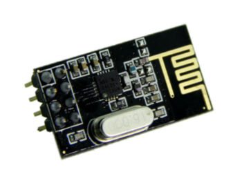
NRF24L01 Transceiver Module
Let’s take a closer look at the NRF24L01 transceiver module. It uses the 2.4 GHz band and it can operate with baud rates from 250 kbps up to 2 Mbps. If used in open space and with lower baud rate its range can reach up to 100.
The module can use 125 different channels which gives a possibility to have a network of 125 independently working modems in one place. Each channel can have up to 6 addresses, or each unit can communicate with up to 6 other units at the same time.
The power consumption of this module is just around 12mA during transmission, which is even lower than a single LED. The operating voltage of the module is from 1.9 to 3.6V, but the good thing is that the other pins tolerate 5V logic, so we can easily connect it to an our board without using any logic level converters. Three of these pins are for the SPI communication and they need to be connected to the SPI pins of the our board, but note that each our board board have different SPI pins. The pins CSN and CE can be connected to any digital pin of the our board board and they are used for setting the module in standby or active mode, as well as for switching between transmit or command mode. The last pin is an interrupt pin which doesn’t have to be used.
So once we connect the NRF24L01 modules to the our board we are ready to make the codes for both the transmitter and the receiver.
The same maintainer has created an OSI Network Layer implementation using nRF24L01(+) radios driven by the newly optimized RF24 library fork.
Protocol used:
This network layer takes advantage of the fundamental capability of the nRF24L01(+) radio to listen actively to up to 6 other radios at once. The network is arranged in a Tree Topology, where one node is the base, and all other nodes are children either of that node, or of another. Unlike a true mesh network, multiple nodes are not connected together, so there is only one path to any given node.
The nRF24LO1+ is a single chip 2.4GHz transreceiver with an embedded baseband protocol engine(Enhanced Shockburst), suitable for ultra low power applications. The nRF2LO1+ is designed for the operations in worldwide ISM Frequency band at 2.400- 2.4835GHz. We can operate/ communicate and the nRF by SPI.
.png)
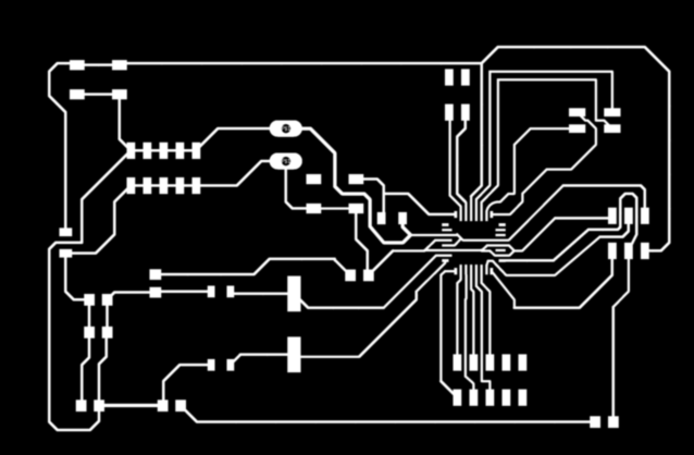
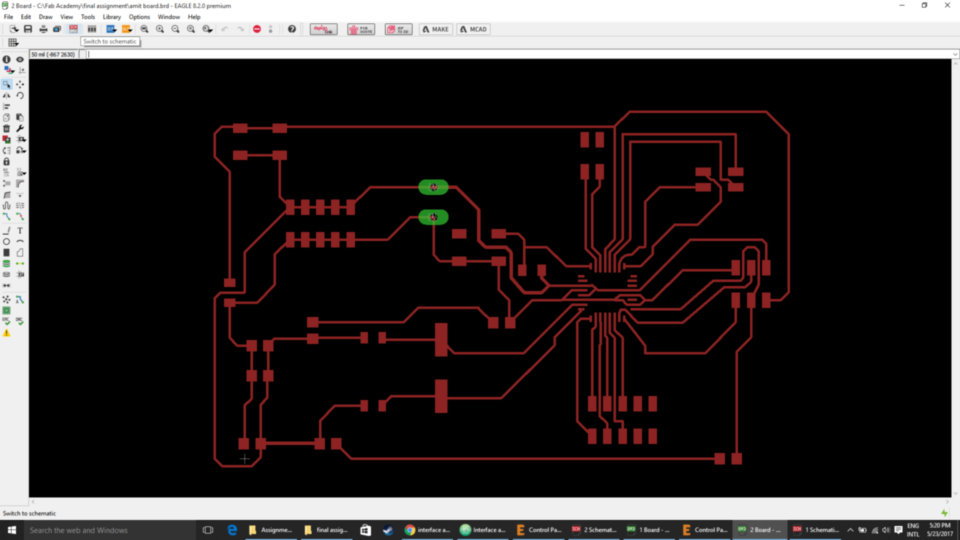
Board File
For this assignment I have used my batchmate gaurang board since I had customize my board according to the project. and I didnt have pins required for this assignment.
- PNG image of the board file which is will be given to the moldela for the PCB fabrication.
 <
<
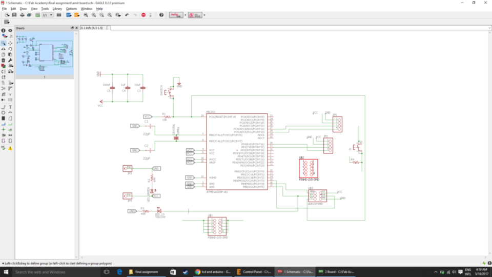
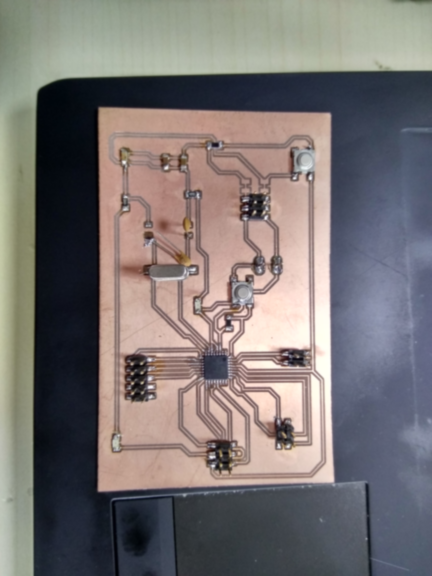
- Board images of the final PCB.
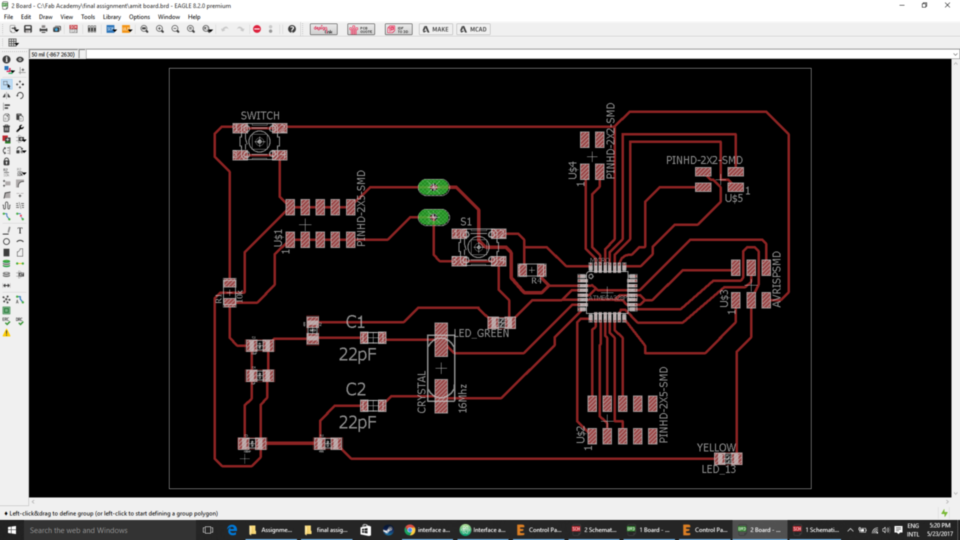
- Image of the board after milled.
Connection:
Connect the following pins to board.
- Pin 9 - CE
- Pin 10 - CS(N)
- Pin 11 - MOSI
- Pin 12 - MISO
- Pin 13 - SCK
- 3.3v - VCC
- GND - GND
- On the Receiver Pin 13 - LED
- On the Transmitter Pin 13 - led same connection for receiver and transmitter board.
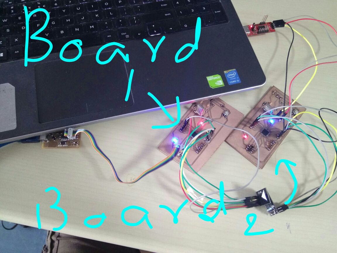
In the image below board one is the transimitter and board 2 is the receiver board.
As soon as the led from board 1 is ON the led from board 2 follows and it ON and when the led is off from the board 1 and then led from the board 2 is also OFF and it follows the board.
Demo Video :