Assignment 6
1.3.2017
Topic: Electronics design
Task:
Redraw the echo hello-world board, add (at least) a button and LED
(with current-limiting resistor), check the design rules, and make
it.
Optional: simulate its operation, measure its operation.
Don't rely on a printed document. Check the information for each
assignment in this living document each week.
Learning outcomes:
Select and use software for circuit board design.
Demonstrate workflows used in circuit board design.
Have you:
Shown your process using words/images/screenshots.
Explained problems and how you fixed them, including how you
worked with design rules for milling (DRC in EagleCad and KiCad).
Included original design files (Eagle, KiCad, Inkscape, .cad -
whatever).
NB. Also, if you make a board and it doesn't work; franken-hack
that board (with jumper wires etc) until it does work, then make a
new one with the knowledge you have gained.
Electronics design tool - Eagle
I downloaded Eagle (8.0.2) software for electronics design
from http://www.autodesk.com/products/eagle/overview
page.
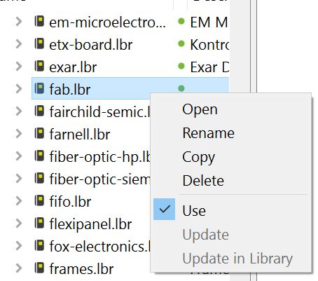
Then, I downloaded fab.lbr component library from Fab
Aademy course page: http://academy.cba.mit.edu/classes/electronics_design/index.html
to folder .../Eagle 8.0.2/lbr.

Then, I selected the fab.lbr library and activated it for
use in Eagle by the second button of mouse.


Then, I created new project and new schematic and ADDed
new components from fab.lbr library. Here I select ATTINY44
microcontroller with SOIC14 package.
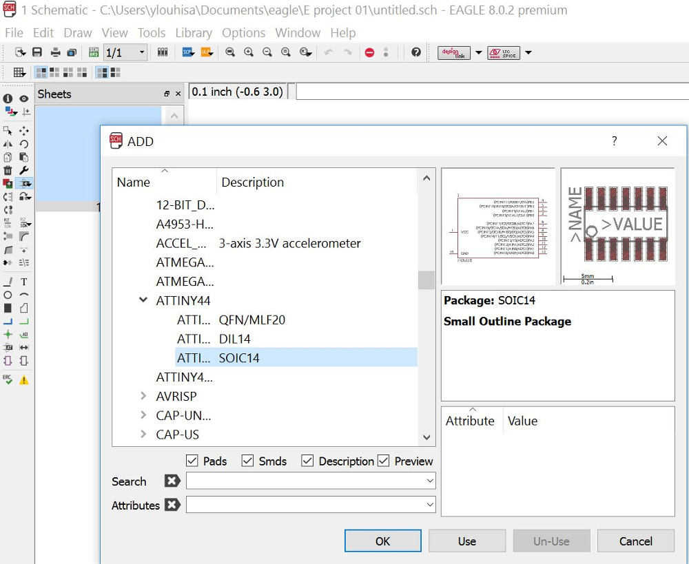
And similarly, I added all components I needed to my echo
hello-world board. I found VCC symbol from supply1 library.
I needed following components:
Attiny44 SSU
Resonator 20 MHz
Button switch
Resistors 1 kΩ and 10 kΩ
Capacitor 1 uF
LED RED
FTDI-SMD header
6-pin connector
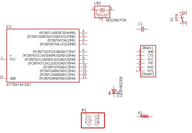
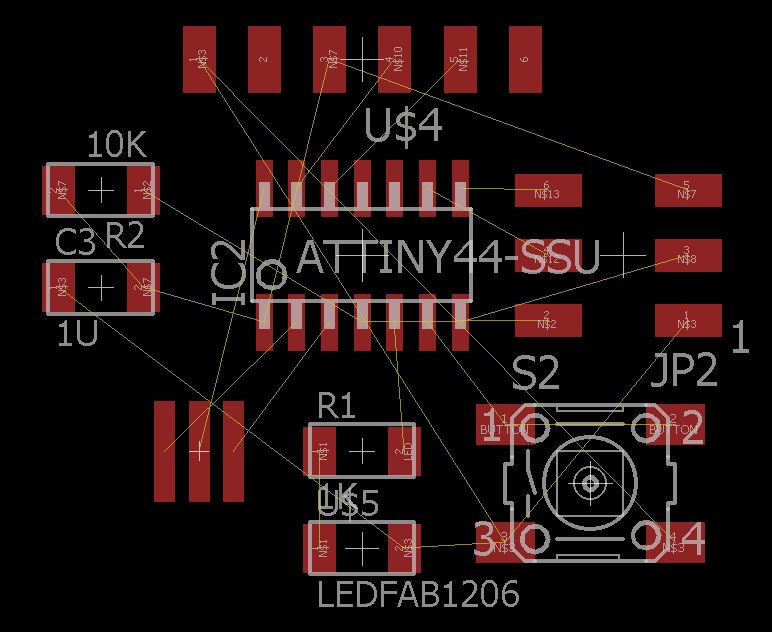
I corrected my plan several times. Here is the final result.
The red line shows the last correction I done manually. Dorina
recommended to use some more components, but I didn't add any
more.
During many iterations, I designed also my board by command: File
> Switch to board. Here is one example of component layout before
routing. I have moved components to working area and further to
optimal places as I thought.
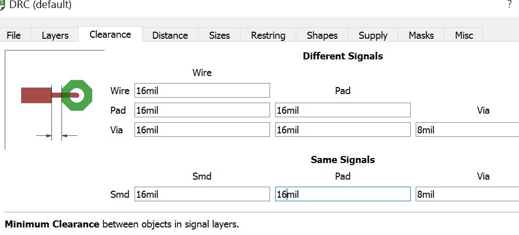
I used DRC tool to set clearances 16mil between components.
Also, I set minimum width of lines to 12mil.
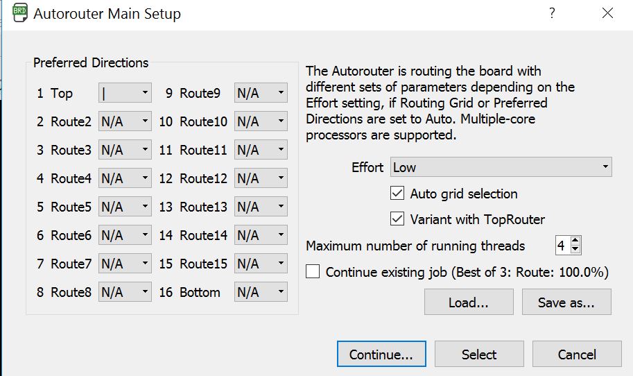
Then, I generated optimal routes by Tools > Autorouter tool.
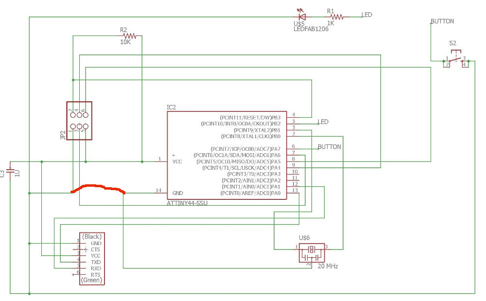
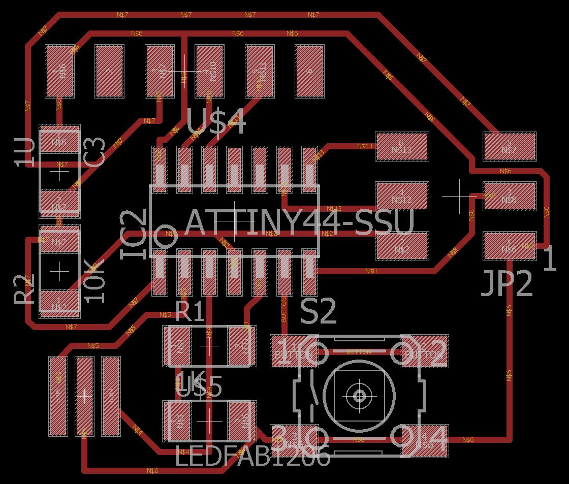
I added zero resistor and removed it. I changed connections of
led and button to the Attiny44 and connected their grounds directly
to other tracks. Also, I changed order of the resonator connections.
After many iterations and corrections, I generated the final result
bellow.
Finally, I checked errors by Tools > Errors tool. No errors.
Now was time to do traces and outlines for milling. I selected only
top layer visible by command: View > Layer settings. Then, I
exported my board as image. I selected monochrome and resolution to
1500 dpi.
Then, I opened the image by Gimp and did cropping by command
Image > Autocrop image. I created a second layer with foreground
color black by Layer > New layer. I increased layer size 1.6 mm
in each directions and centered the image by command Layer >
Layer boundary size. Then, I extended the image size to layer size
(Fit canvas to layers) and changed layer order. Next, I enlarged
image size to fit all layers by command Image > Fit canvas to
layers, made borders black by filling the empty area by black color
and saved the image as hello-traces.png.
Similarly, I made area inside borders white and saved the image as
hello-outlines.png. The board
size was about 27x25 mm. These png files updated later as I tell at
the end of this page.
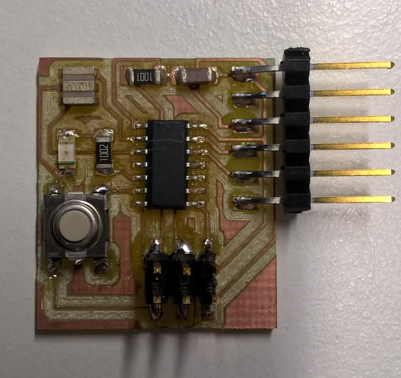
Board milling and soldering
I used again fabmodules.org page and generated
milling files for Roland SRM-20. Now, I used v-shaped bit
for traces milling and it made very clean-cut. Then, I used pick and
place machine and reflow oven for soldering of small parts. A button
and connectors I soldered by hand.
Testing
 I tested the operation of my board and
programmed a short blink program. I used Arduino IDE environment and
Arduino UNO as ISP programmer.
I tested the operation of my board and
programmed a short blink program. I used Arduino IDE environment and
Arduino UNO as ISP programmer.
Arduino UNO board needed Arduino ISP program. I added also Attiny
board support to the IDE.
And as a result, the board blinks the led slowly and if I
press the button it blinks fast. Also, I used my Fab Tiny ISP
programmer with Arduino IDE and it worked well.
One important issue is the need of external power +5 V. Fab TinyISP
doesn't provide power for board to be programmed.
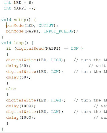
Arduino pins were: 12 MISO -- VCC
13 SCK --
MOSI 11
10 RE
-- GND

Original Eagle files are here:
schematic
board layout
Post-registered note:
I made a new board, because power pin from FTDI-SMD header broken
out. I cut the 2x3 connector from 2x5 piece and cur too near the
pin.
New board is little bigger. The 6-pin connector seat now correctly
on top of board. And, I soldered FTDI-SMD header in bit wrong place.
I took it out, replaced it by new one and made little repair,
because foil was damaged during took-out.
However, here we go!
This new design is presented as png files as following: hello-traces6.png and hello-outlines6.png.