Electronics Design
Tasks:
Select and use software for circuit board design
Demonstrate workflows used in circuit board design
Redraw the echo hello-world board, add (at least) a button and LED (with current-limiting resistor), check the design rules, and make it
Two weeks ago, we produced our own PCB board, using the already premade design. This week, we are going to design our own board.
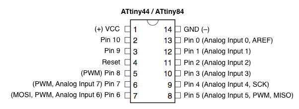
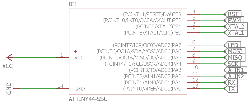
My #1 Guide for making the PCB was the ATtiny44 pinout
The software which I will be using for this assigment is 
EAGLE (Easily Applicable Graphical Layout Editor) is a flexible and expandable EDA schematic capture, PCB layout, autorouter and CAM program. EAGLE is popular among hobbyists because of its freeware license and rich availability of component libraries on the web.
Eagle has two windows that are used simultaneously to design a board:
- Schematic (.sch) - logical components
- Board Layout (.brd) for the actual board that we mill
After I installed EAGLE, the first thing which I want to do is Create a New Schematic. A schematic in electronics is a drawing representing a circuit. It uses symbols to represent real-world electronic components. The most basic symbol is a simple conductor (traces), shown simply as a line. If wires connect in a diagram, they are shown with a dot at the intersection.
In order to place my components on the schematics, I have to download and use special Libraries. Eagle has a lot of built in libraries of components that we can use. The fab network also maintains a library which is constantly updated:
In order to install the library, in the EAGLE environment, go to the top toolbar and select the Library menu. Then select use and open the .lbr file that I just downloaded.
Now I can go to Add component and selecting the library, I choose the component which I want to place.
I will start with the microcontroller ATtiny44
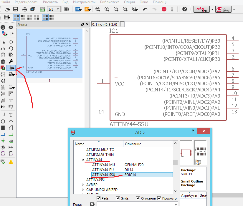
I repeat the same process with all the components which I am planning to use. Here is the list of components that I used:
- ATtiny44 microcontroller x 1
- Cystal 20MHz x 1
- Capacitor 10 pF x 2
- Resistor 499 Ohm x 2
- Resistor 10K Ohm x 1
- LED x 2
- SMD Buttons x 2
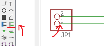
When I have all the components placed on my schematics, I have to connect each of them to the pins of the microprocessor. In the EAGLE left menu, I click on Net, command which allows me to draw green lines and connect the pins. Important thing is to start the connection from the little line on the pin (I marked it on the picture)
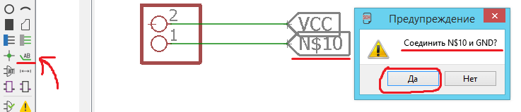
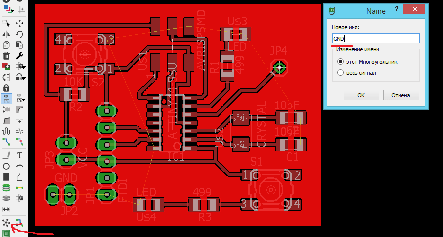
To avoid multiple connections, I will be using Labels.. In EAGLE left menu, I press Add Label and add it to the end of my connection line. If I press the right click and then choose name, I can attribute to the label the same name which I used for the microprocessor pin, and connect them in this way!
If I did everything right, a message should appear that states: Are you sure you want to connect your label (N$10) with GND?
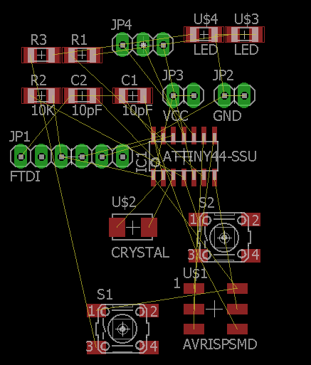
At this stage, in the chematics, the important thing is the Logic of all connections, not the way it looks. After I finished placing all the components, and connected them in a logical way, this is how it looks:
On the left side of the microcontroller, I placed the VCC and GND component, and connected them with the processor.
On the right side, I connected all my components using labels.
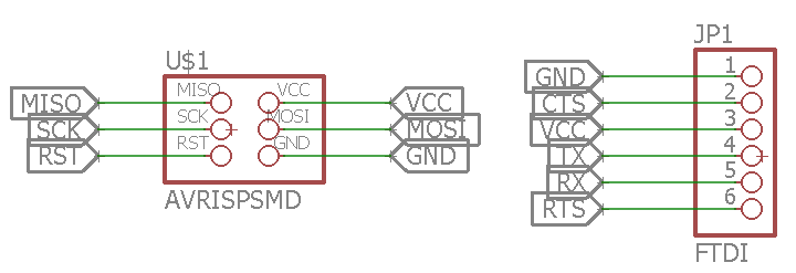
I added the AVR_ISP pinheaders, and placed them in according order for the connector. These pins will be used to program my board.
I also wanted to add the necessary pins for the FTDI cable, which has a USB to serial converter inside, and will allow me to easily upload the code. I can use the FTDI cable to program it later, but it is only for the communication as the programmer will be the PC (this is related to the way that Arduino is programmed having the bootloader installed) .
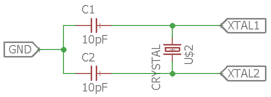
This is the circuit for the 20MHz crystal, reinforced from both sides with 10pF capacitors, and connected using labels to the microcontroller.
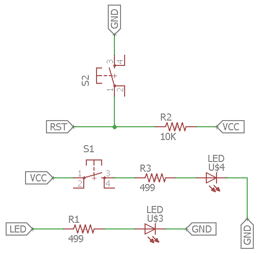
I also placed two LEDs. One will be controlled by the SMD button, another by a digital pin called LED.
When I press the button, the LED is on, when I release the button, the LED is off. The same from the digital pin. When I send a signal to the digital pin HIGH, the LED will shine, and vice versa
I also placed a button, which has the function to reset the board, accompanied by a 10K resistor.
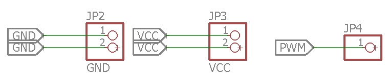
I also added some additional pins, just in case. Two VCCs, two GNDs, and one Digital Pin (PWM).
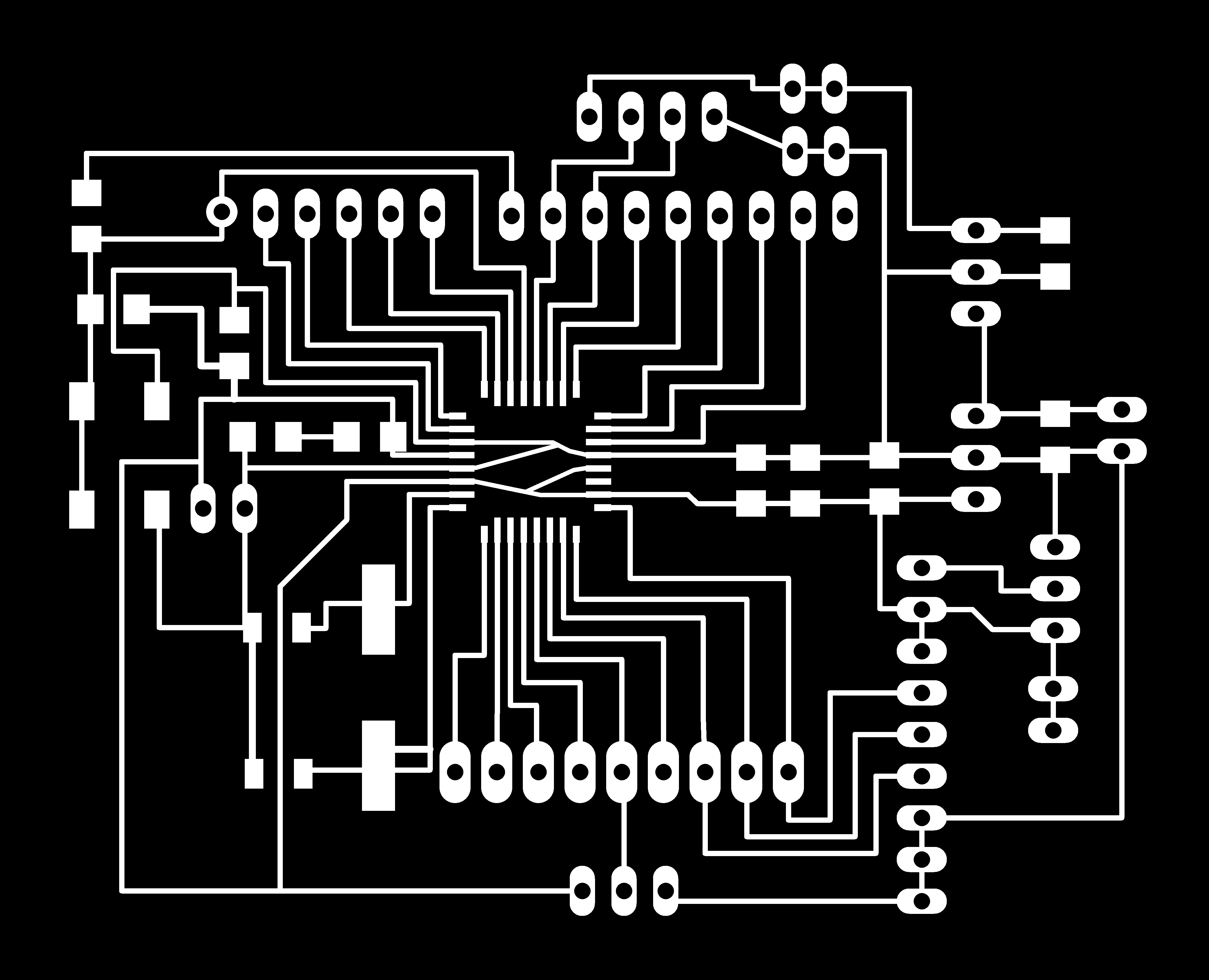
After I double check all the connections, I can proceed to the next step, which is the Board Layout. On the top menu, I press Generate/Switch to Board. And this is what I get, a BIG MESS of connections.
I know that it looks like imposible, like a puzzle with endless combinations, but its actually not as complicated as it looks like.
Because I have a little experience with EAGLE, I have got kind of feeling, or sense of how to deal with this. I little of experience and practice, will make the routing way easier.
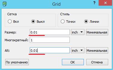
First thing which I do is increase the Grid resolution. I go to Viewmenu, and press on Grid, and change the values to 0.01. This will let me be more precise while drawing the route lines.
And now the Fun Part begins.
After about one hour, I managed to finish everything. I am using a little trick here.
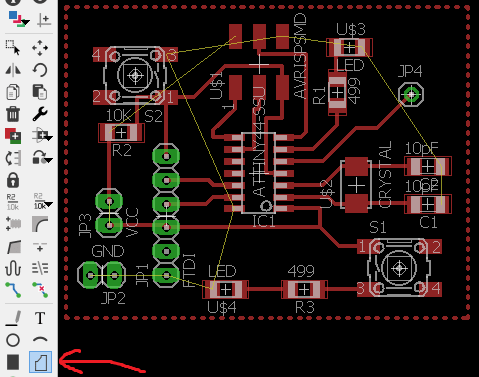
The trick is to leave all the GNDs unrouted. I draw a polygon arund my components, and pressing the right click on the polygon line, I change the name on GND. This will fill the whole area inside the polygon, and make it to be the GND.
This will save a lot of time, space, and effort
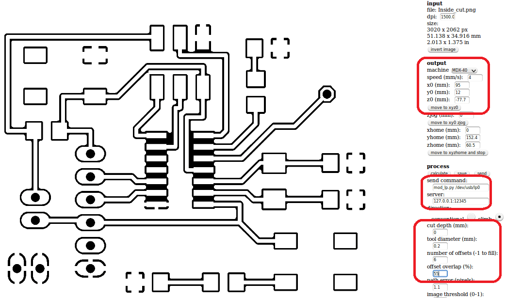
When I double check everything, I can Export my file as a .png picture.
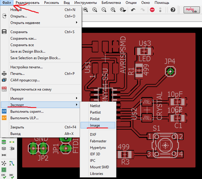
In the appearing window, I increase the resolution to 1500 dpi, click on monochrome, and select window mode.

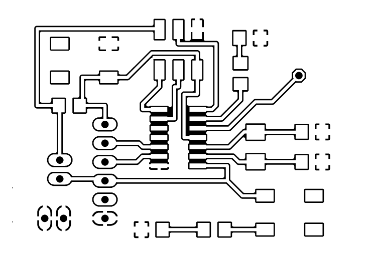
To edit the .png image, I will be using  I open my image in GIMP, and using the
 rectangular select tool, I select the image leaving some space from all the sides. After I press File and Copy the selected area. To continue working with the selected picture, I click again on File, and Create from the Clipboard
This is what I get:
This image is ready to be printed, and I will call it Inside_Cut
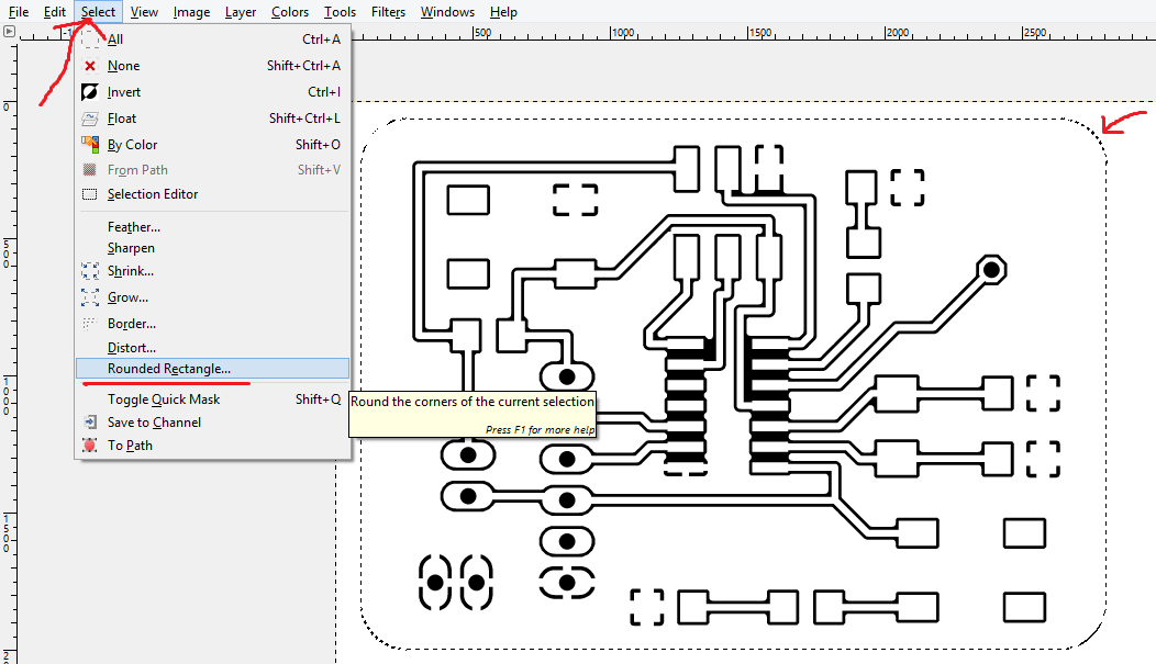
To print the outside cut, I select the image again using the rectangle tool, and on the main page, in the Select menu, I press rounded rectangle and choose the radius to be 20. Because the copper material on which it will be printed is sharp, I make some fillet to round the corners
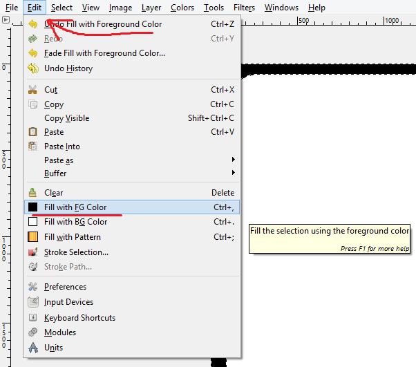
In the Edit menu, I choose to fill the inside of the selected area with BG color.
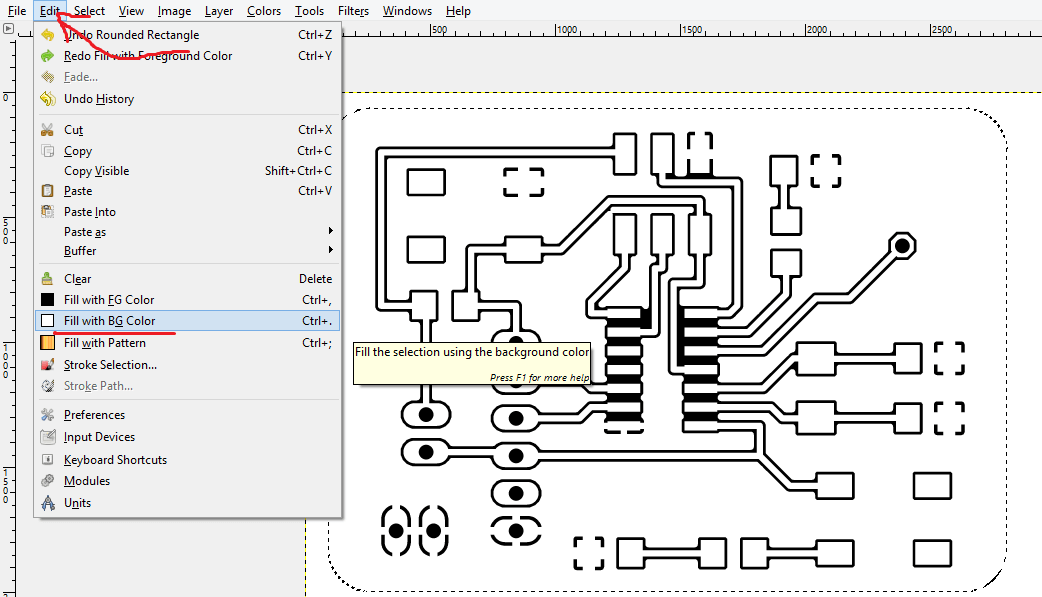
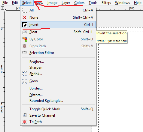
In the Select menu, I invert the selection, and fill everything with the black color.
The result image I save as Outside_Cut
Now I can proceed to the CNC milling machine. So, again I used FabModules to convert the .PNG files into Gcodes for the Roland machine.
Let’s start to work with the Fab Modules. When I introduce the ip adress into the browser window, the first interface that will appear is:

After I press on th gray button input format, a new menu should appear with the option to load the .PNG image. Here I upload the first image, which is the inside engraving. After doing that, the preview of the image will appear in the Fab Modules and also other fields and other parameters will show up
On the right side of the window, we have many input parameters. In order to be able to move the machine, we have to input the following parameters:

mod_lp.py /dev/usb/lp0 into the send command field
hostname_of_your_machine into the server field (just the address without http or /)
In order to move the machine I just enter in the respective fields the x, y and z position coordinates. Before moving the machine I have to make sure that the zjog parameter is always set to 0, even if it will change automatically. To move the machine I have to press the move to xyz0 button.
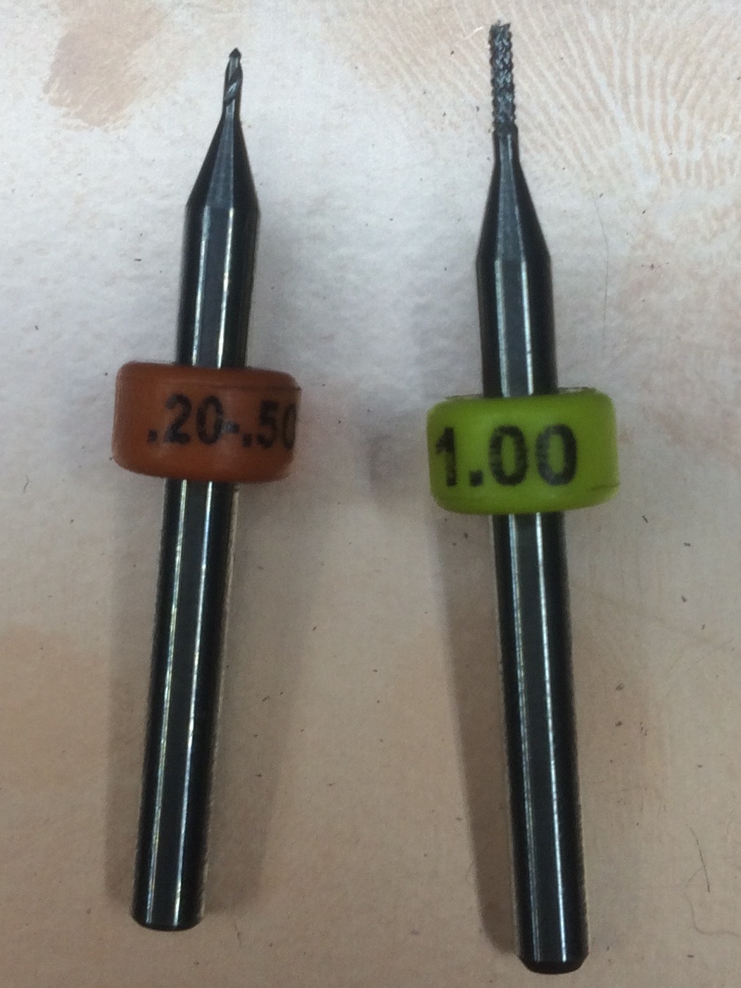
* A small life hack is to use the multimeter and check if there is connection between the tool and the surface. As a tool to engrave PCB is suggested to use diameter from 0.2 mm and below, while for cutting we can use a 1 mm tool.
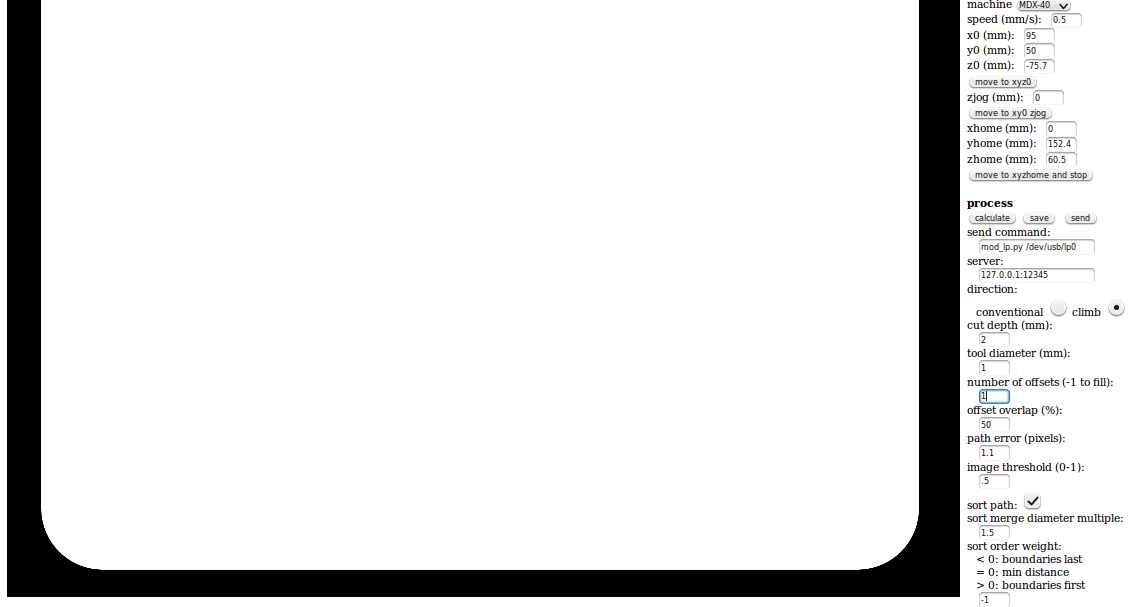
So my final settings look like this:
Problem:
When I pressed the Calculate button, I got a very weird result:
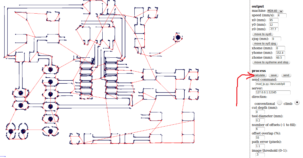
Even though I had number of offset - 6, it did not look like the maschine was going to make it.
I realized that my problem was back in the EAGLE design.
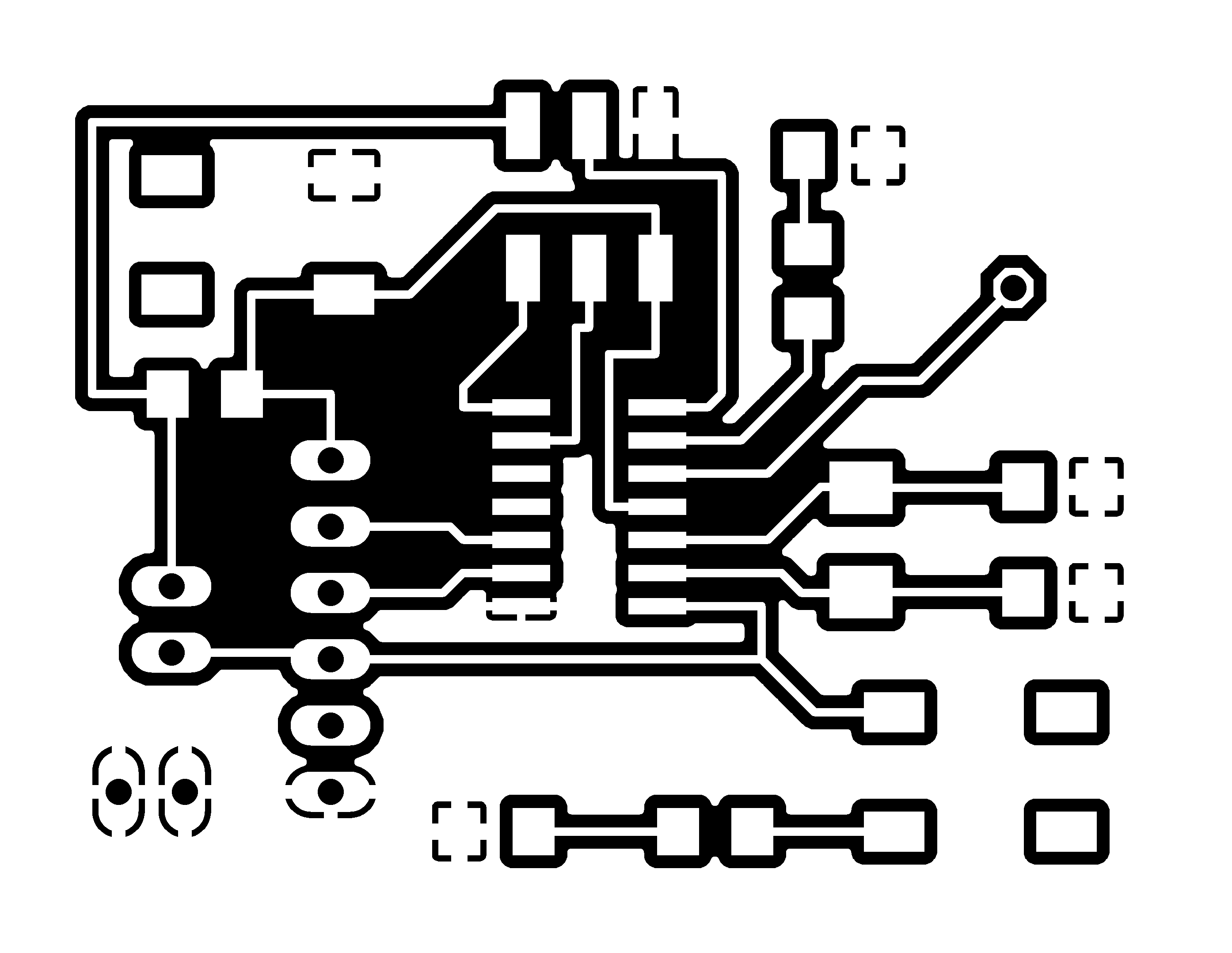
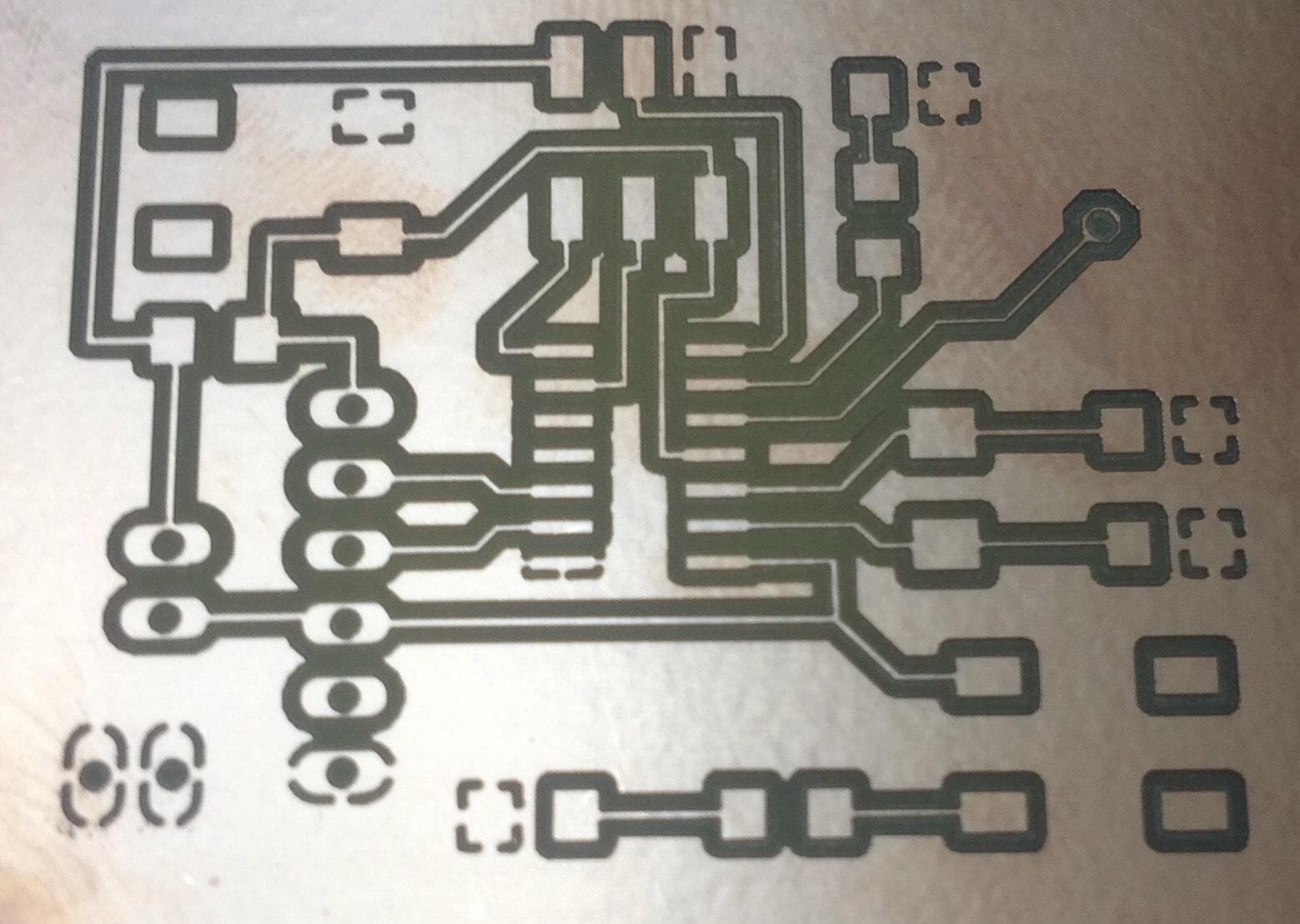
To solve the problem, I increased the Isolation to the value of 0.2. And after I went again through the whole process of exporting and editing the image, the picture looked diferent:
The calculation of the FabModules looked way better now:
Now I can send the job to the maschine.
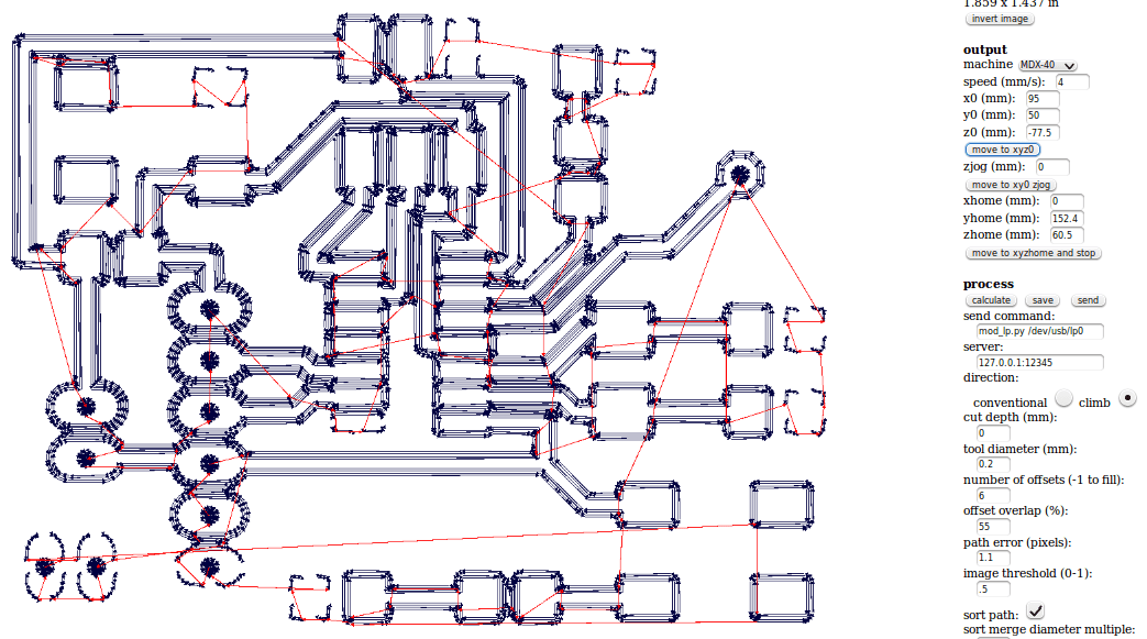
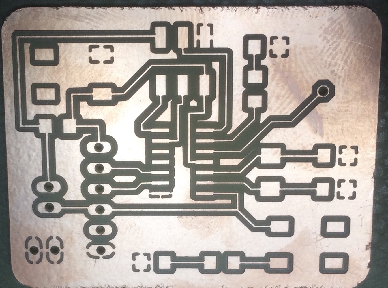
For the outside cut the settings remain the same with the exception of the value of the Z-Axis, as I replaced the 0.2mm tool with the 1mm tool, and the parameters of the CAM. This is how it looks:
This is how the final result looks like:
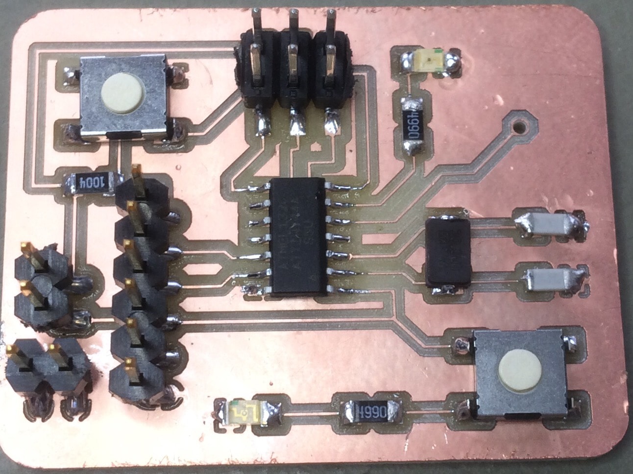
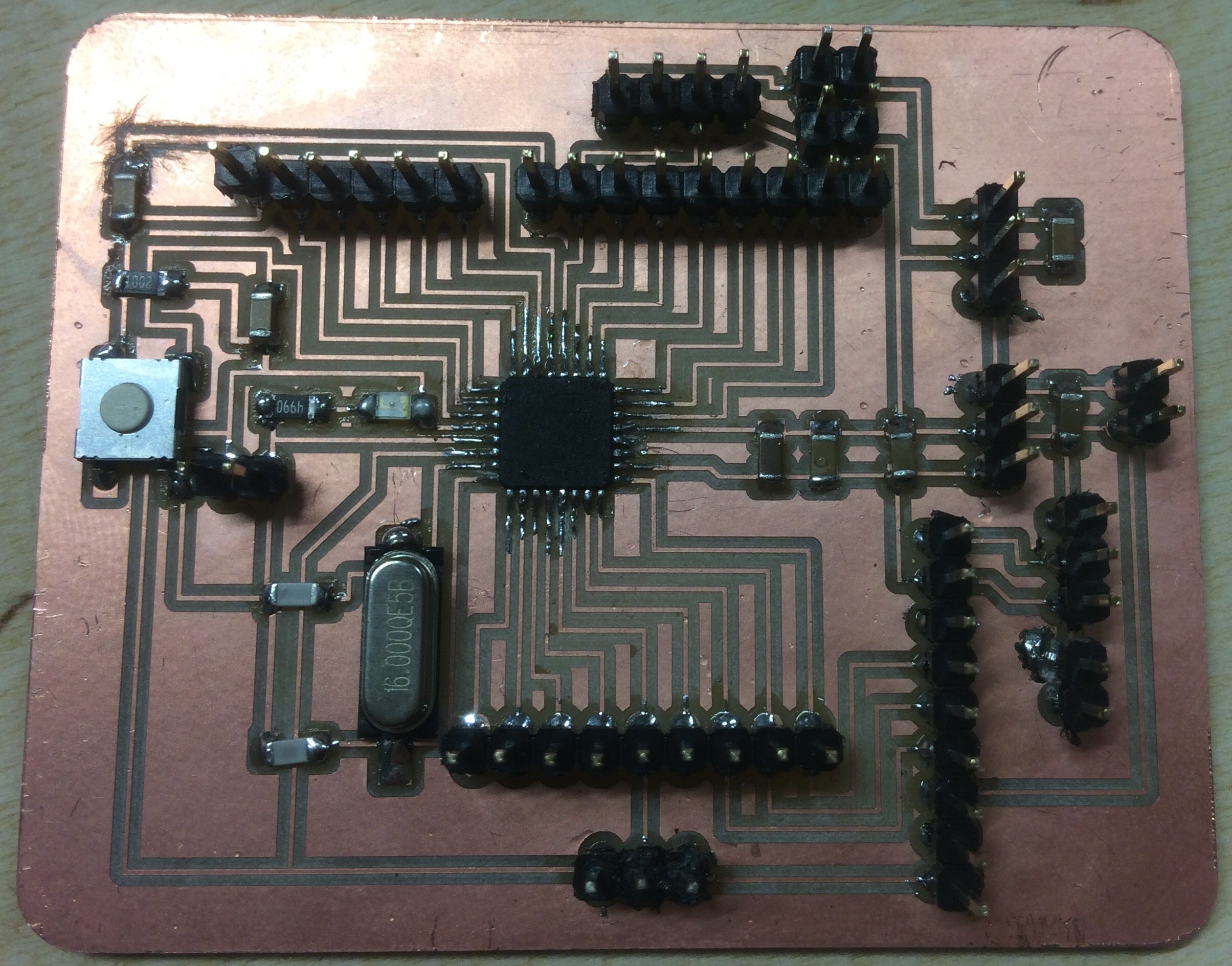
And now Let's solder this!
In order to make sure that I soldered everything in a right way, after each component soldered, I used the multimeter to check if there is conductivity between the component and the traces.
This is my final PCB
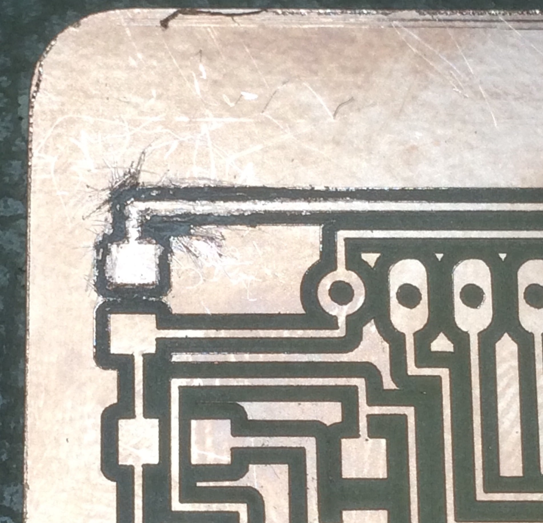
After I soldered all the components, I noticed a small mistake. The button from the left side of the microcontroller, one pinout is supposed to be connected to the GND. Because I increased the isolation, the whole area under the button became isolated, and created kind of an island which is not connected to the GND.
The same thing happened to the GND pin of the microcontroller, it got isolated, and because of this, nowhere is GND anymore.
Because of the time pressure, I decided to fix the problem rather than milling another PCB. This is how I fixed it:
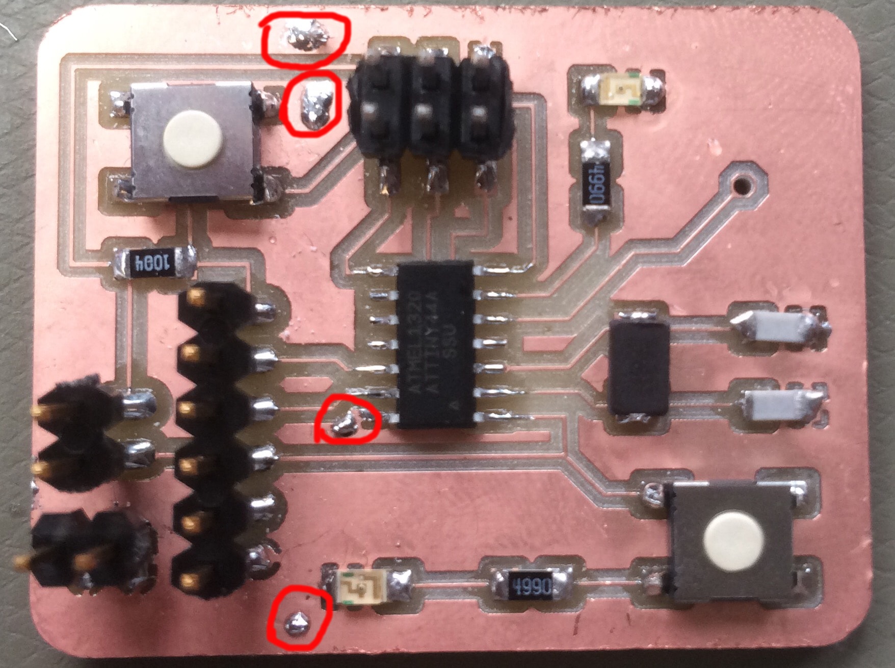
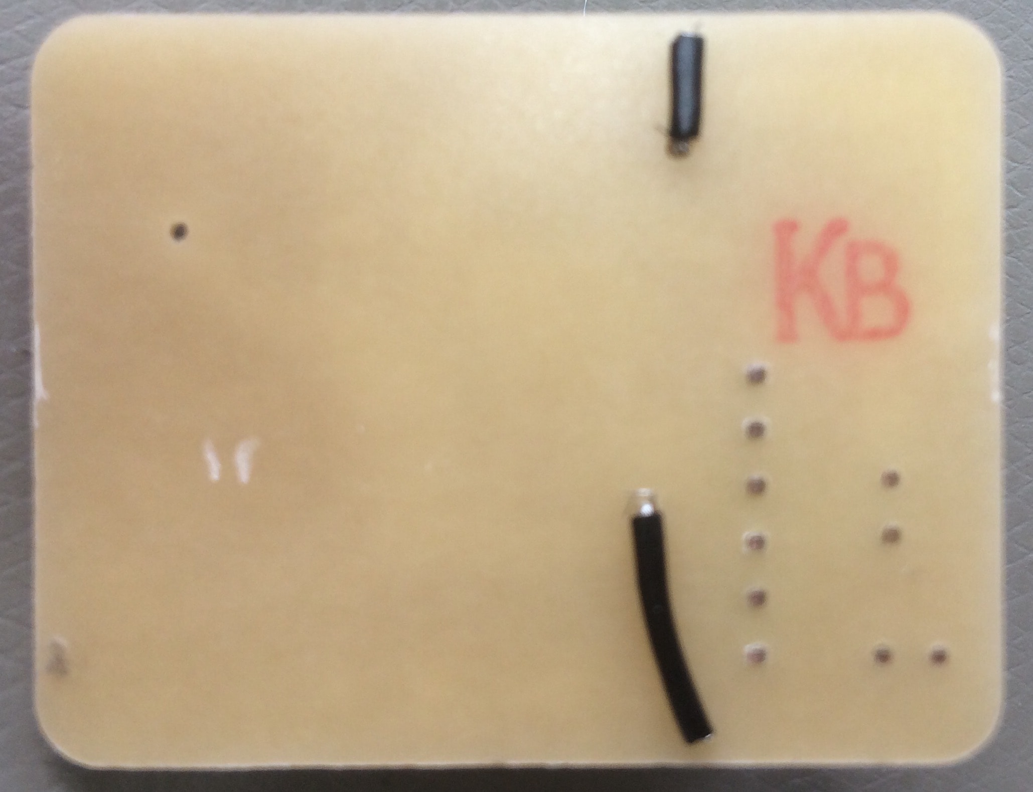
I drilled two holes, and connected them using wires at the back of the board. Now, I have GND everywhere it is supposed to be
Just look at this. Isn't it beautiful? :D
The next step is to Program It! Now I have only a board with some components on it, but let's give it LIFE. The software wich I am using is  , an open source software which allows to program Arduino boards. And yes, in order to program a board we have to use another board; its like Egg / Chicken situation - what appeared first :D
To use the Arduino board, I had to patch it in advance adding the Attiny44, detailed instructions can be found HERE. After I patched the Arduino IDE, I connect my arduino board to the USB hub, in the tools menu select the right board (Arduino Uno/Genuino) and the port, after go to File--> examplesand open the Arduino as ISP sketch. Upload the code.
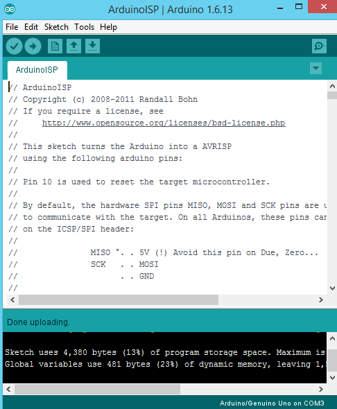
After I see done uploading, which means that the code is uploaded to the board, I disconnect the arduino from the PC. The next step is to connect my PCB board to Arduino using some wires. The connection scheme is this one:
- SCLK: Serial Clock (output from master).
- MOSI: Master Output Slave Input, or Master Out Slave In (data output from master).
- MISO: Master Input Slave Output, or Master In Slave Out (data output from slave).
- VCC: Positive supply voltage.
- GND: Ground.
- RST: Reset.
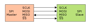
The right connection is very important, otherwise it is possible to damage the board. That is why, after I triple check the connections, I can go on setting the parameters for the Arduino IDE. I connect the arduino board to the USB hub, and select the right board/processor/frequency -> ATtiny24/44/84, ATtiny44, internal 20Mhz. Under Tools select Arduino as ISP programmer, double check the parameters, and press the Burn Bootloader button.

After everything is done, we can upload any code to our PCB board. I chose a simple example code Blink. It will make the LED blink for 3sec, switch it off for 3sec, and then switch on again, and so on for ever :D. The important thing is to choose the right pin, in my case Pin 7.

Here is a short video:

Its BLINKINGGGG!!!!
Download Files:
Past Experience
I would also want to mention that in the Fundamentals of Digital Fabrication course, which was organized by the FabLab Kamp-Lintfort as an introduction to the Fab Academy, I created my own board, by modifying the already existing Satshakit board. I would like to share my experience about that!
I created the PCB based on the already existing model called Satshakit. It is an arduino UNO replication board, which I modified according to my needs. In order to make the future wiring of all the components easier, I decided to place all the needed pins for one sensor next to each other, and have an organized connection.
The sensors that I used were BMP180 Barometric Pressure Sensor, DHT11 Humidity & Temperature Sensor, and the Graphic LCD 12864B for my future Weather Station!
To design the board, I was also using EAGLE.
This is how the final satshakit + my modifications looks like:
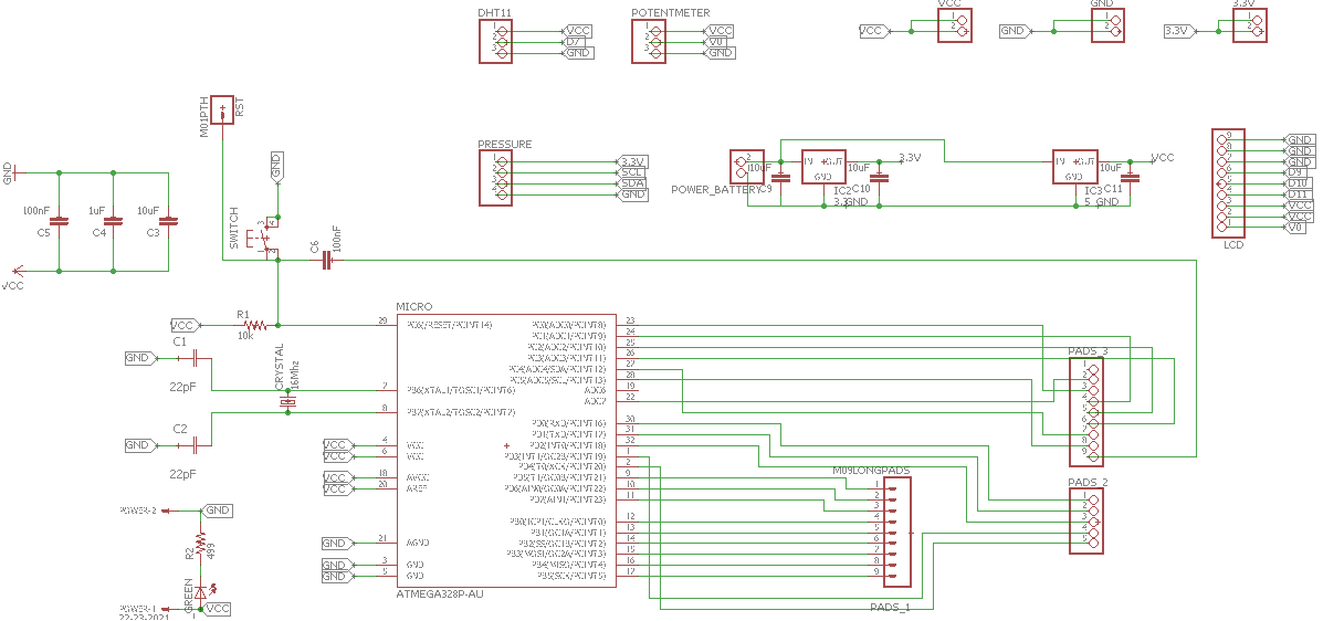
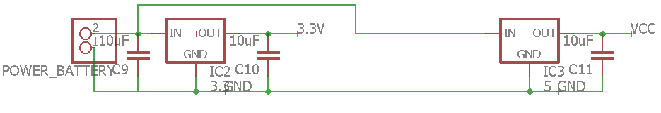
I will repeat mysel that on the first page of the EAGLE it is important to have the right Logic of all the connections. The thing which I added first is a voltage regulator with an input from the 9V Battery, and two outputs: 5V and 3.3V. I also placed two 10 microfarad capacitors in order to assure the stability of the voltage regulator.
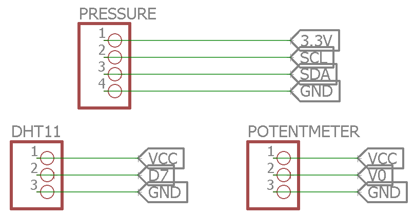
As I mentioned before, I want to place all the necessary pins of the sensors next to each other, to make an organized and easy wiring. I placed some pin headers for the DHT11 sensor, BMP180 pressure sensor, and the potentiometer , and connected them to the corresponding pins on the microprocessor using some labels. I am not sure if I want to use the potentiometer to regulate the contrast of the LCD Display, but I decided to place the pins anyway just in case.
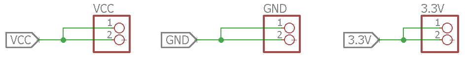
I also added some additional pins for 3.3V and 5V power supply, and some additional GND pins, in order to have my board ready for any new crazy ideas that may come to my mind :D
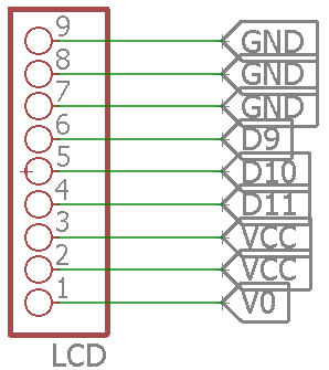
And the last but not least, I added all the necessary pins for the Graphic LCD Display. This thing takes a lot of pins, and If I do not think of organizing the wires, it will make a big mess in the whole system. The LCD uses 3xGND pins, 3xDigital pins, 2xVCC pins, and V0 pin for the contrast regulation.
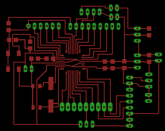
My final board layout design looks like this:
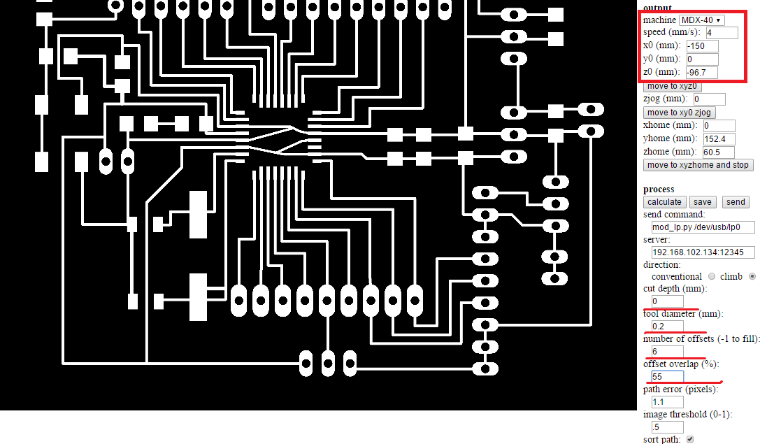
I also used FabModules to mill the PCB. These are the settings that I used:
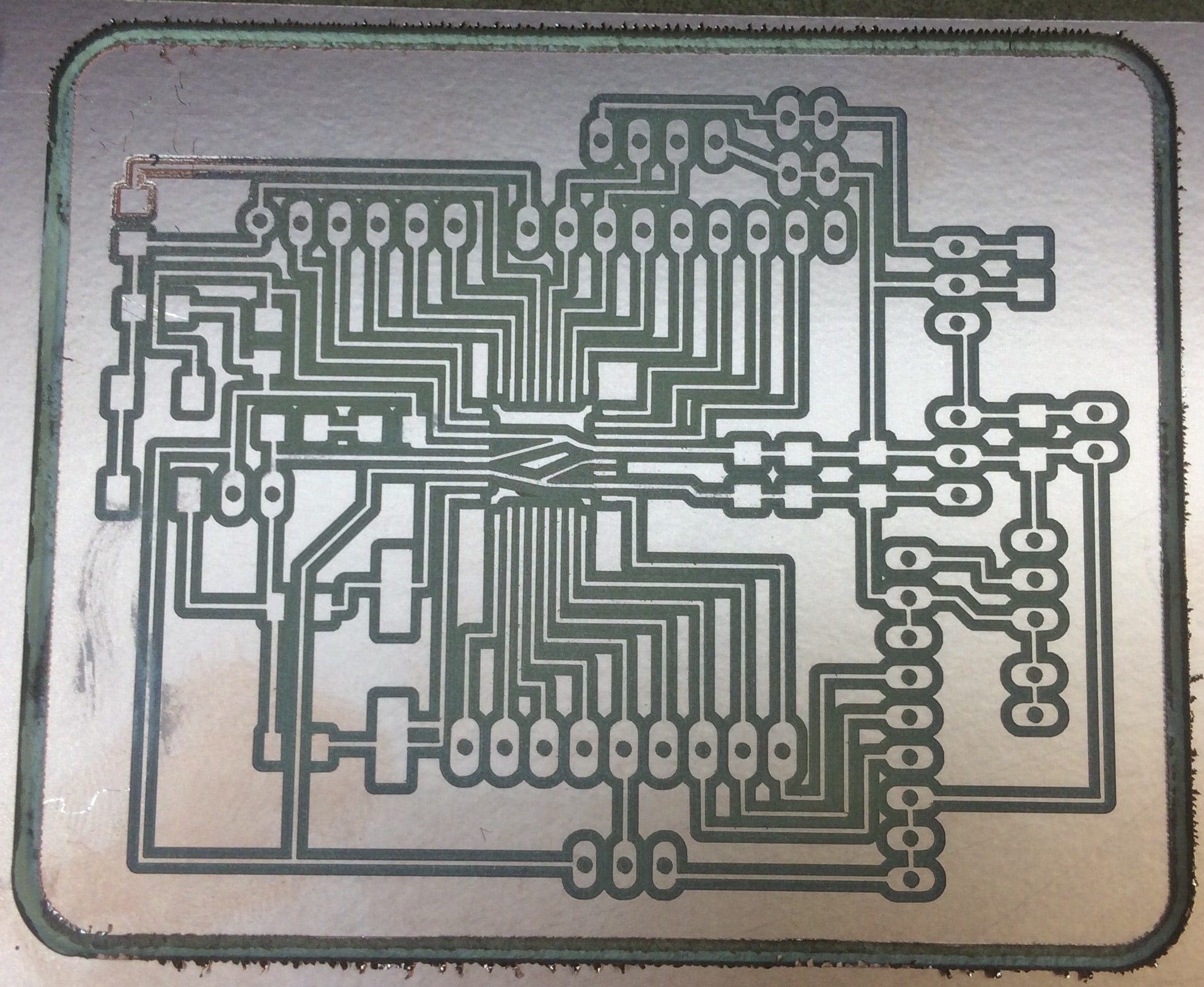
Because the board is big, to mill it took quite long, but the result was good:
Problem:
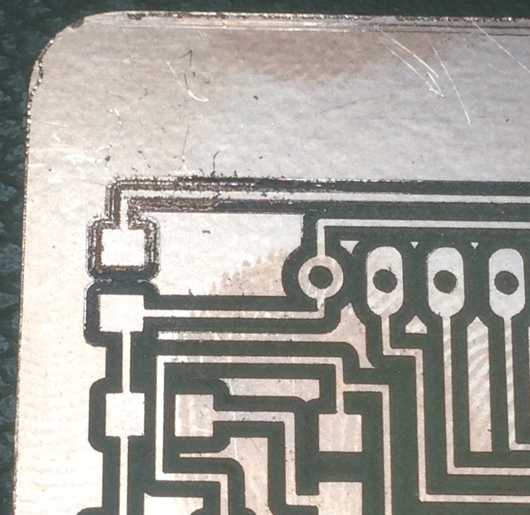
Analyzing the draft circuit, I noticed that one corner of the circuit is not well done, and I think this is due to the fact that the plate was not equally flat. I decided to continue with the outside cut, and then fix the problem by hand.
After everything was fixed, It's time to solder! The most difficult part, and the most important one was to solder the microprocessor. The problem was that the traces are so small, that I was soldering two traces at the same time, after which I had to separate them. In order to make sure that I soldered everything in a right way, after each component soldered, I used the multimeter to check if there is conductivity between the component and the traces. Honestly saying, the begining was hell, but after 2 hours, I really liked soldering :)
And Here We Are!
Download Files:

