Electronics Design
For this week's assignment, It was required to:
1. redraw the echo hello-world board.
2. add (at least) a button and LED (with current-limiting resistor).
3. check the design rules.
4. make it, and test it.
To first start with task, I went through previous students' websites. This is always a good step for start to review previous work and successes, failures and recommendations. Fab Academy Electronics Design 101 course was a great reference to start with.
Next, I reviewed Echo Hello board in details, understood the components and read a little bit about ATTiny44 and its pins.
Before I start implementing on Eagle, I reviewed Electronics Design in the tutorial section to have a quick overivew on the start.
To implement your board on Eagle, you need few steps:
1. Sketch your board in Schematic view and connect the components.
2. Switch to board view and arrange your components.
3. Route your components.
4. Check your board by ERC (Electical Rules check) and DRC (Design Rules Check).
5. Prepare your board for machining as previouly done in Electronics Production week.
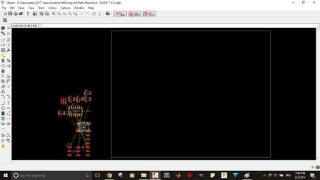
I. Sketching the board:
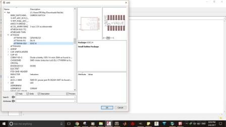
I started by importing Fab library to eagle to use the components in it. Start adding components using "Add" one after another till you get them all. PS: I worked directly on adding the LED and the switch to the board.
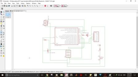
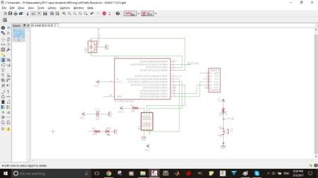
I, first, sketched the circuit as it is and then added the Led and switch.
After adding the components, connect them using the "wire" option. Sometimes, connections get messy; so as optimization, name your connections you want to connect together using same names and you'll find eagle asking you if you want to connect themm; click "Yes".
For that, use "Name" command. This is will make your schematic look a little bit neat, and it will be more organized.
Finally, to avoid confusion, add "label" to connections.
 |
 |
| First Sketch | Modified Sketch |
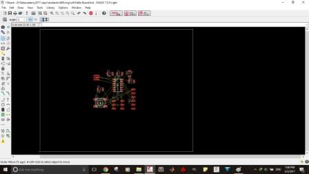
Next Moving to Board View.
To switch to board review, just click on that button  . It asks you if you want to generate the board out of the schematic, click "Yes".
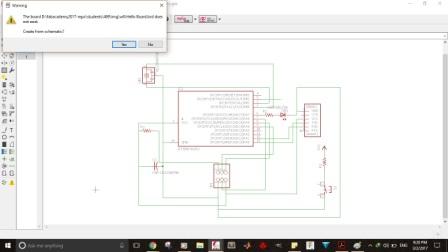
The board is generated with all components are outside the frame and only connected with a yellow line as a guide from your connections in the schematic. Re-arrange it the way you want inside the board.
 |
 |
| Components in brd view. | Re-arranging components. |
Now, It's time to connect the components. For this, you use the "Route"  command . My first attempt was to try the "Autoroute" option, it calculates the best way to route your board. Results were NOT actually very satisfactory.
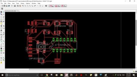
I dicovered a stupid mistake while working on the board, and it's that I mistakenly added the Through hole version of ATTiny44! and to change change, I needed to replace it by the SMD one. You can simply do that by the "Replace"  command ; and Done!
Routing your circuit is the hardest part of the process; you need to find the best path to your tracks, taking in consideration clearance for not to have a short circuit or wrong connections in any way, but I was getting there and Finally Done!
II. Checking Rules:
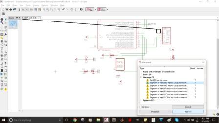
It's important after you finish your board to make 2 important checks:
- ERC: stands for Electrical Rules check; where you check all your connections and make sure everything is correctly connected.
- DRC: Stands for Design Rules check; this is simply to make sure that the machine can machine your board and there is enough clearance and no overlap in traces.
1. ERC:
To perform Electrical rules check, just click on ERC button 
Doing the check, I got some warnings, but they were all "components are not physically connected"; so it was not an issue as they were connected already but in a neat way.
2. DRC:
To Perform Design Rules Check, I used the file provided by Neil and Fab Academy. You can download it from here.
Click on DRC button  ; uplad your the file to set your parameters and click "Check"
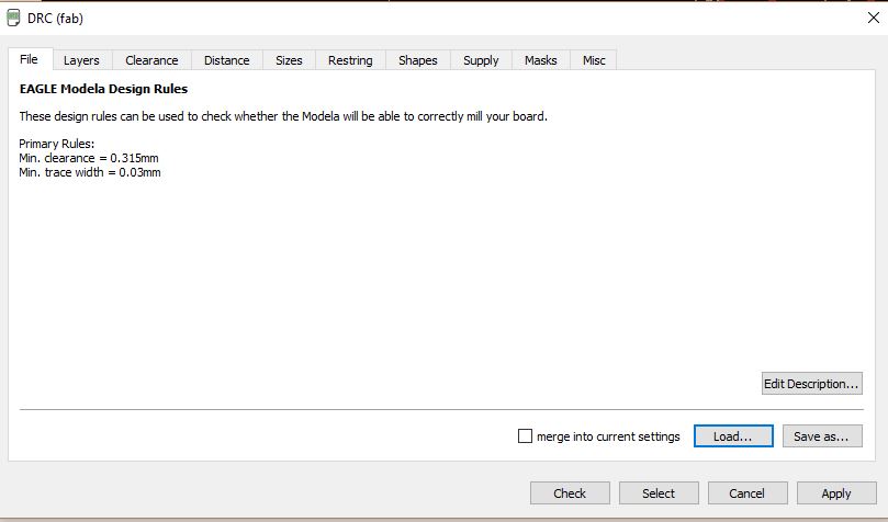
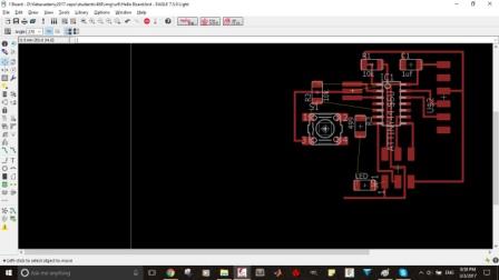
I had some error in clearance, and I tried to solve it by trying different routing, but It didn't work. I ended up shrinking the width of some traces route from 0.4064 mm to 0.3048
| Error in Clearance 1. | Error in Clearance 2. |
 |
|
| Error in Clearance 3. | Error Fixing. |
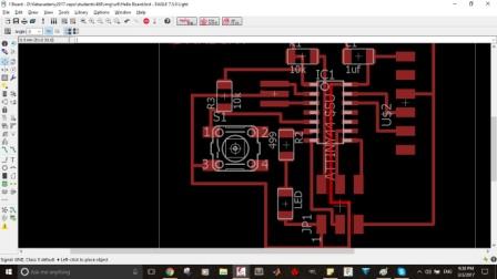
Last thing I did was to add my name on the board.
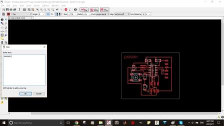
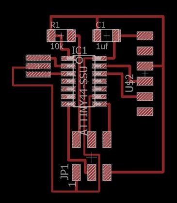
That how it looked at the end.
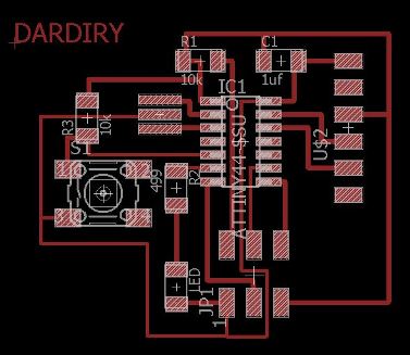
And this is how I redraw the original circuit.
 |
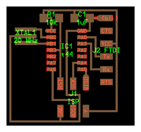 |
| My design. | Original Circuit. |
III. Prepare your board for machining:
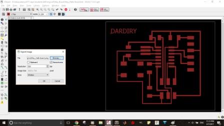
1. Exporting your picture:
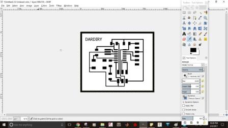
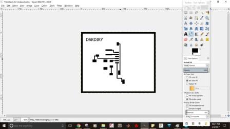
a) In your layers settings  , show only your traces to make it look like the below picture.
b) Export your circuit to a PNG monochromatic picture with a dpi not less than 500. I did mine with 500 dpi.
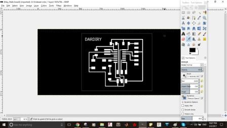
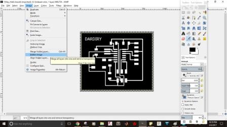
c) Go to Gimp or any picture editor like Illustrator and others for final editing. You'll need to add a border to your file and prepare your traces file to mill and border file to cut it.
d) Open your image in Gimp and crop it till you are only left with the frame of the circuit.
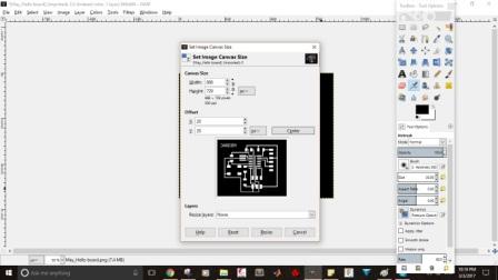
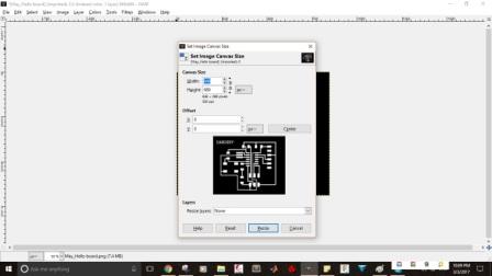
e) From Image in task bar, choose "Canvas size". This will add to space to your image. Add 40 pixels to width and height and center your image; finally click "Resize"
f) Final Step is to "Flatten Image"; this will color the added space with a color. You can choose whether with the forground color or background one. We need to color it in White anyway, and most probably it's the background color
 |
 |
| Opening Picture in Gimp. | Canvas Size. |
 |
 |
| Adding Borders. | Flatten Image. |
Now, traces are ready! Export your image and save it. This is how it's gonna look like.
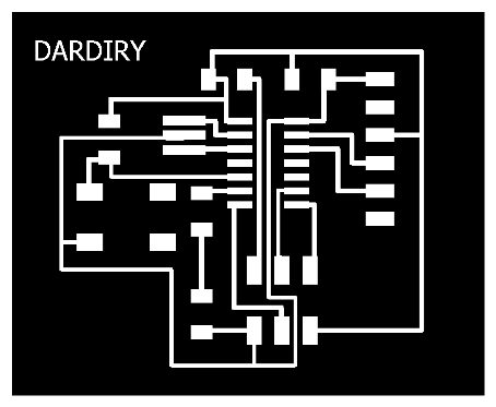
To prepare your borders, invert your image using "Value Invert" option in Colors list. Use the brush to color all internal traces in white, so you are only left with the border.
 |
 |
| Value Invert. | Coloring inner traces. |
Now your border is ready to export! This is how it should look like.

V. Milling your board:
1) Traces:
Open Fab Modules and select "image (.png)" as your input, "Roland mill (.rml)" as your output format, and finally, "PCB Traces (1/64)" as your process.
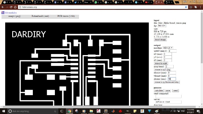
Next, choose your machine, and adjust your X0,Y0 & Z0. Also select the appropriate number of offsets (usually between 1 to 3), this indicates the number of times the machine is gonna go for to remove the copper. I used "2".
Last step, Click "Calculate" to show your path
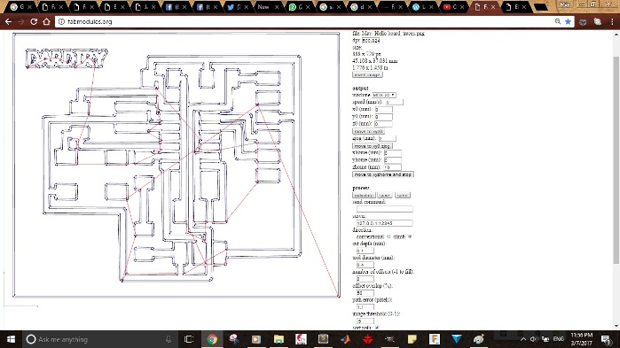
And Now, send to the machine. If you are using MDX 40A or SRM 20, save the rml locally and use V Panel to mill the traces.
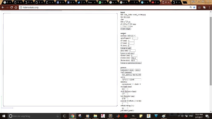
2) Borders:
Replace your mill bit to 1/8 one to cut the board, and zero your machine.
Repeat what you did for the traces, with changing "PCB traces (1/64)" to "PCB outlines (1/32)".
And Here you go!
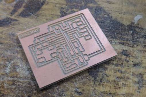 |
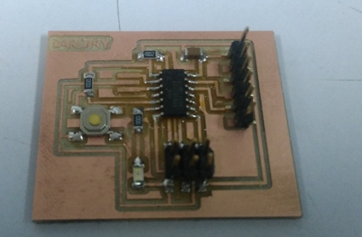 |
| After machining. | Stuffing the board. |