Assignments
#1 Redraw the echo hello-world board
For the first time using the Eagle application and for the first time designing my own PCB... So below I will try to explain the way I processed.
- Step #1
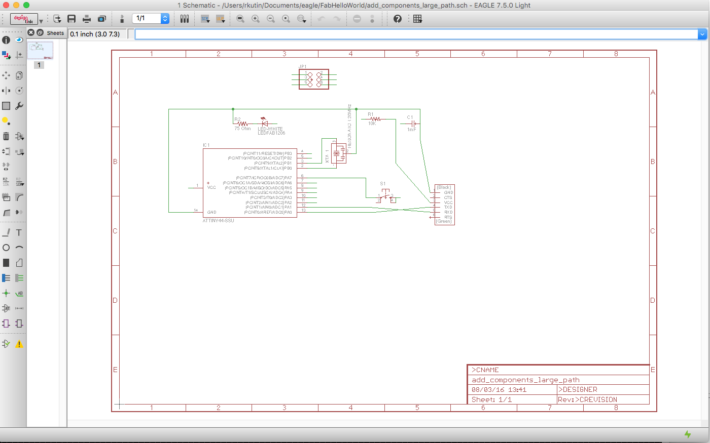
- Elements to principal schema. I started by visual identification for the elements on the photo of the board. As well I had the pcb image on which I saw that the top small elements are the resistor on 10 Kohm and the capacitor on 1 mf. So after the identification of all the elements I create new project in Eagle and created the A4 area on it. After I found in library and placed all components on the principal schema in the Eagle application.
- Step #2
- Wiring principal schema Let do wires on all elements. I started by connecting all pins to good locations. To avoid the many cross-wires I used following method. I added small wire to each of pin that has clear function and name the main wires connections by functions. So I added RST, VCC, GND, MISO, MOSI connections (so not many cross-wires now.)
- Step #3
- Initial PCB. When all connections were done - I executed some tests to be sure that all components are wired and that no errors on schema.
- Step #4
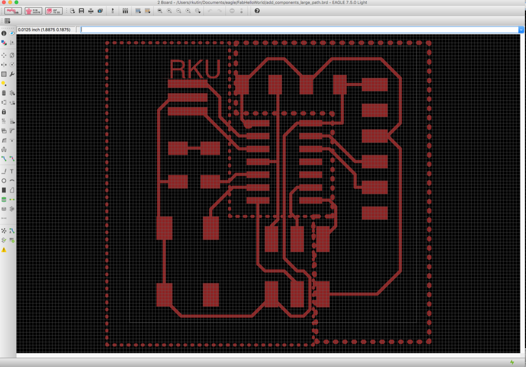
- Recreate path. Now we need to create path on PCB. This is a first try on creation path so I don't really care about the design rules except the one that I want all path on the same side. So I did it.
- Step #5
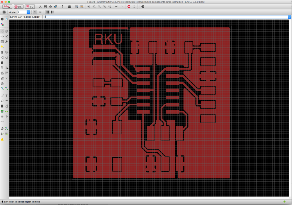
- Apply design rules. Now I try to make tuning of my PCB by applying the design rules and moving components and paths to be ok with that. Here are some of rules I applied.
- #1
- Path better to turn on 45 degrees.
- #2
- Think about speed of CNC machine. So less copper you need to remove - faster your PCB will be produced.
- #4
- No small distances between the two copper path in hidden places. If I will have difficulties to access to some path and during the soldering I will put some overdose of soldering pasta - it may create short circuit and I will be not aware about it. So under the chip - less risks as possible.
- #5
- Size of our drill bite is 1/64 inch - so distances between the path should permit to pass a drill.
So let see on results.
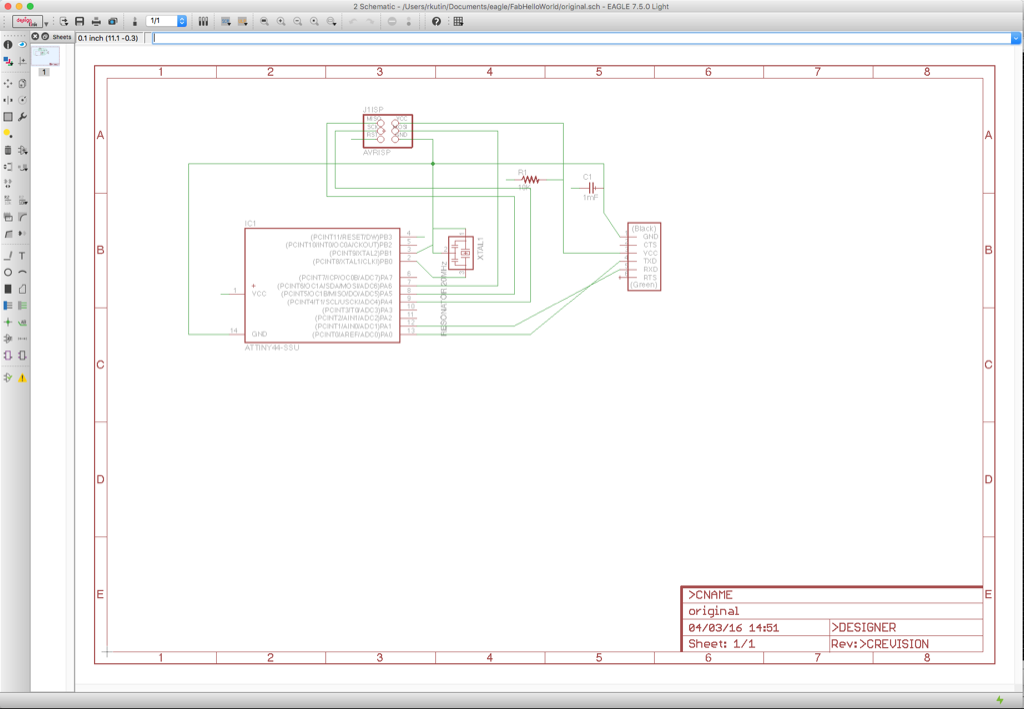
Original board schema
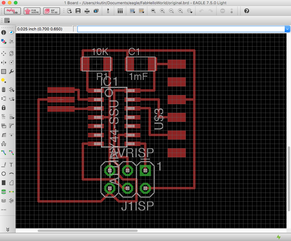
Original board pcb
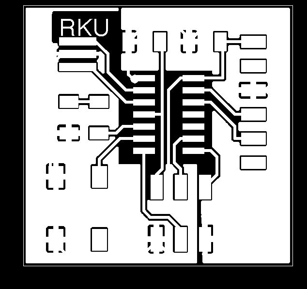
When I did my PCB I realized that we do not have in inventory the crystal so I recreated my board to have a crystal that we have in inventory + 2 capacitors. Below is the result.
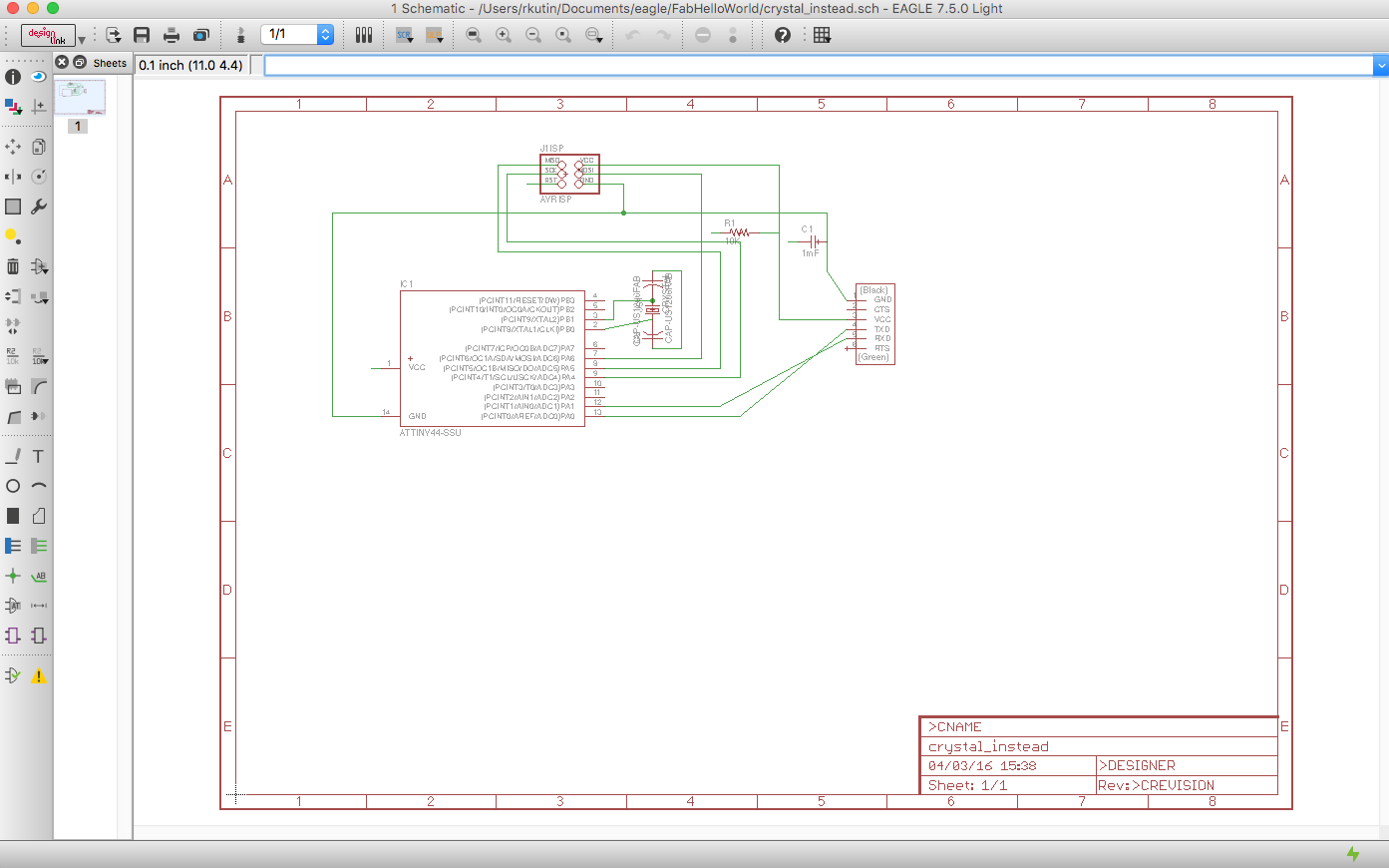
Board with crystal
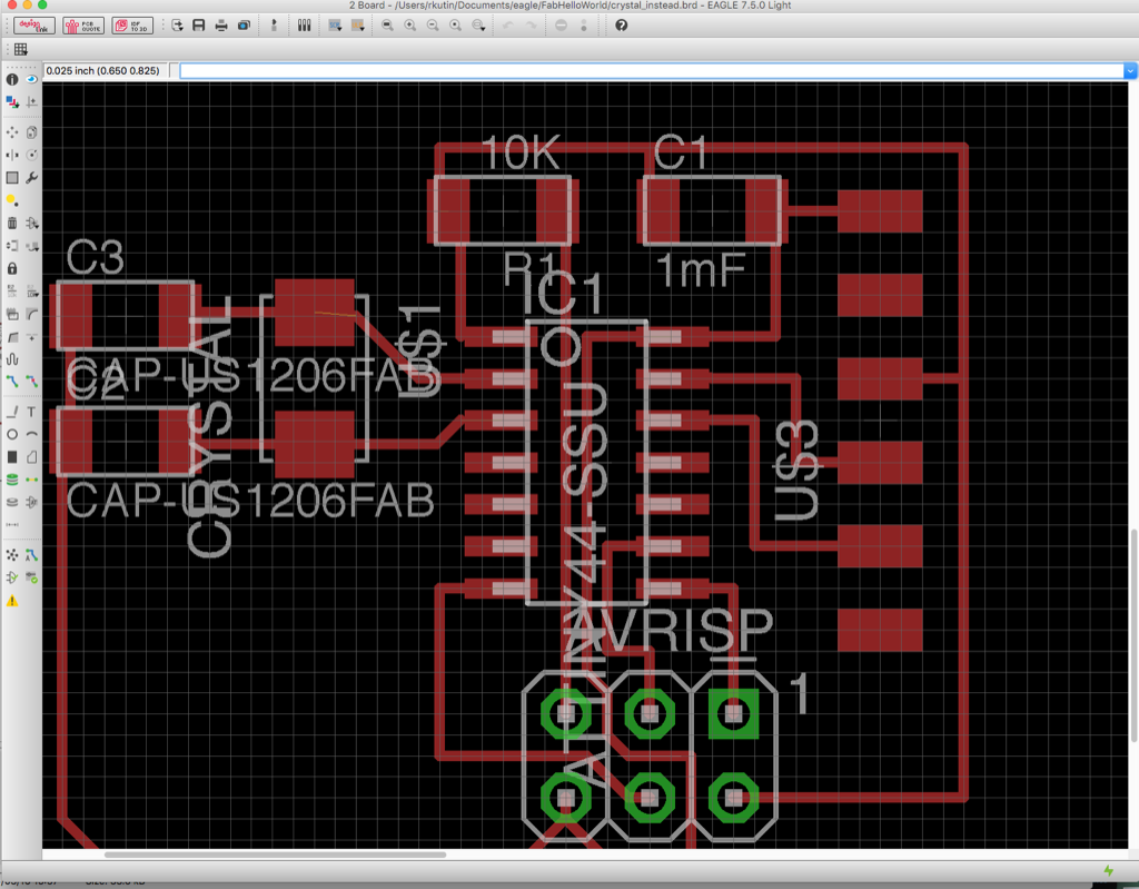
Board with crystal pcb
Assignments
#2 add (at least) a button and LED (with current-limiting resistor)
To add a button and LED I did following steps. I checked the data sheet of the LED and found that 3.5V is tension and 20mA of intensity. As well looks like that on output from the pin ATTiny will produce 5V. So after my calculation I need to add a resistor of 75 Ohm to have correct intensity arrived to LED.
Button I attached to ATTiny between one of the pin and the ground. Looks like that ATTiny has a capacity to attach pull up resistor and VCC to the pin... Let see how it will works.. :).
After applying the design rules I have following card. You can see that I used polygon to GND and VCC on final view and I aligned it to avoid zone under the chip...
Schema with button and led
Board with button and led
Use polygon for GRN and VCC
And the PNG in monochrome that can be transformed to SVG and used by our VCarve application for our CNC machine.
Milling path

Cutting board
Assignments
#3 check the design rules, and make it
This week I could not pass to FabLab to produce the card. But I decided to create (after the 3D printer from kit) the little CNC machine (or even as I will not create a lot of PCB I probably can use my 3D printer as CNC milling machine.) So I tried to generate the G-Code that can be taken by my 3D printer and probably draw my card. (Not sure that result will be published this week, may be the next one..) But let do the code.
First I did export of my PCB to Gerber and to Excellon formats. These files will be used by the FlatCAM application.
When We loaded file in FlatCAM - we generate then milling path by applying parameters of milling machine. After this I saw that my PCB in fact can not be simply milled by 1/64 milling bite. It can not create some path because of too close locations. So I re-optimized path and did it again. Now it is better.
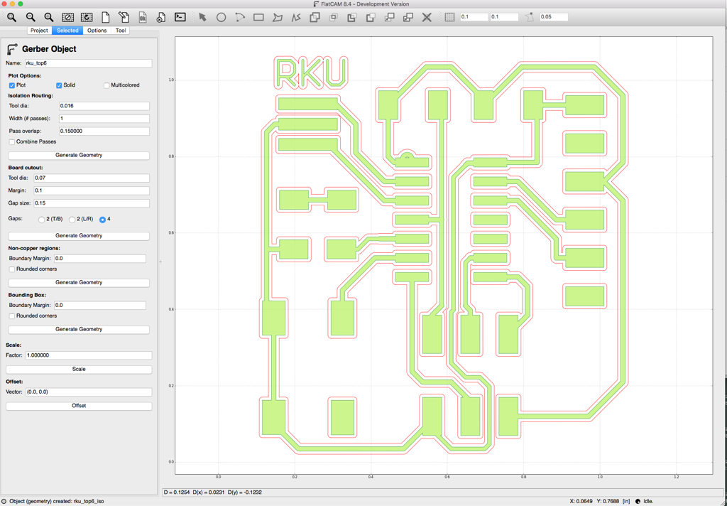
Milling path generated
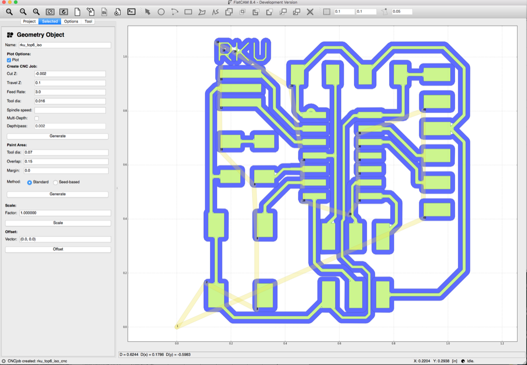
Now we see in gcode path
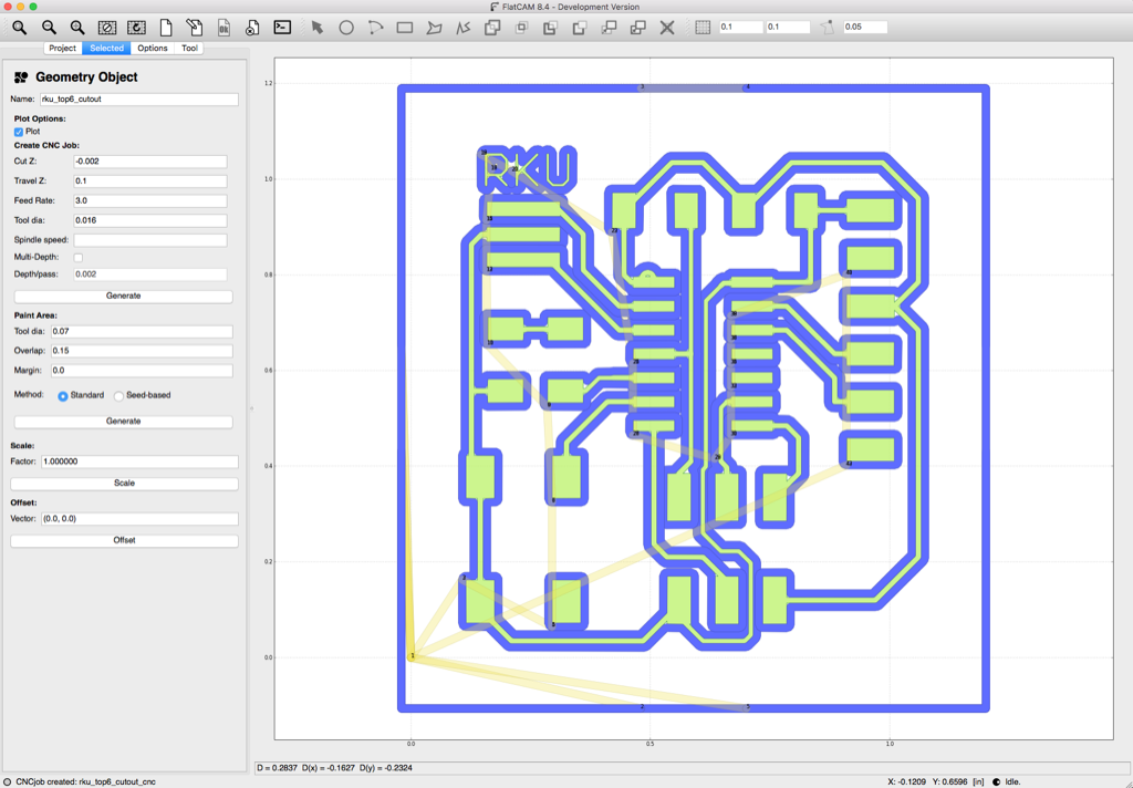
Adding the cut-off path
The next challenge is to run this code on my 3D printer (at least with the pen...)
Assignments
#4 extra credit: simulate its operation
To make simulate functionality of attiny I used 123D circuits site. So I added the power + attiny + 1 capacitor + 1 resistor and LED and make it works... It just blinking for the moment. Now I am searching how the attiny manage the button.
Here is the code that permit LED blinking... Button will arrive soon...
              int led = 0;
              int button = 1;

              void setup() {
                // initialize the digital pin as an output.
                pinMode(led, OUTPUT);
                pinMode(button, INPUT);
              }

              void loop() {
                // if (digitalRead(button)==HIGH){
                //   digitalWrite(led,HIGH);
                // } else {
                //   digitalWrite(led,LOW);
                //}
                if (digitalRead(button)==HIGH){
                  digitalWrite(led, HIGH);
                  delay(300);
                }
               digitalWrite(led, LOW);    // turn the LED off by making the voltage LOW
               delay(300);               // wait for a second
              }
You can try the simulation by open My project and click "Start Simulation"